On-Chip Plasmonic Slit-Cavity Platform for Room-Temperature Strong Coupling with Deterministically Positioned Colloidal Quantum Dots
Jin Qin, Benedikt Schurr, Patrick Pertsch, Daniel Friedrich, Max Knopf, Saeid Asgarnezhad-Zorgabad, Lars Meschede, Daniel D. A. Clarke, Monika Emmerling, Artur Podhorodecki, Ortwin Hess, Bert Hecht

TL;DR
Researchers developed a compact on-chip platform that enables strong coupling between quantum dots and plasmonic cavities at room temperature.
Contribution
A deterministic fabrication method for plasmonic slit-cavities with colloidal quantum dots is introduced for room-temperature quantum technologies.
Findings
Photoluminescence-resolved Rabi splitting was observed at room temperature in precharacterized plasmonic cavities.
Device-to-device variations correlated with the average number of coupled quantum dots.
Integration of electrodes enabled electrical tuning, though limited by spectral diffusion at room temperature.
Abstract
Strong coupling between quantum emitters and optical cavities underpins many quantum photonic technologies, yet achieving this regime at room temperature in compact, deterministic on-chip platforms remains challenging due to the difficulty of fabricating cavities with ultrasmall mode volumes and precisely positioning quantum emitters. Here, we demonstrate a robust quantum plasmonic device in which colloidal quantum dots are strongly coupled to plasmonic slit cavities. Our dielectrophoresis-based positioning technique with real-time photoluminescence feedback enables parallel device fabrication and straightforward integration with additional optical elements, such as waveguides. Our measurements reveal clear photoluminescence-resolved Rabi splitting at room temperature in precharacterized cavities, with device-to-device variations scaling with the average number of coupled quantum dots.…
Genes, proteins, chemicals, diseases, species, mutations and cell lines named across the full text — each resolved to its canonical identifier and authoritative record.
Click any figure to enlarge with its caption.
 2
2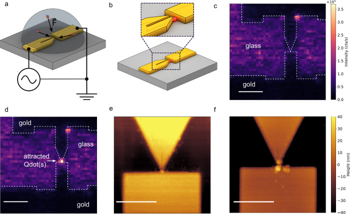 3
3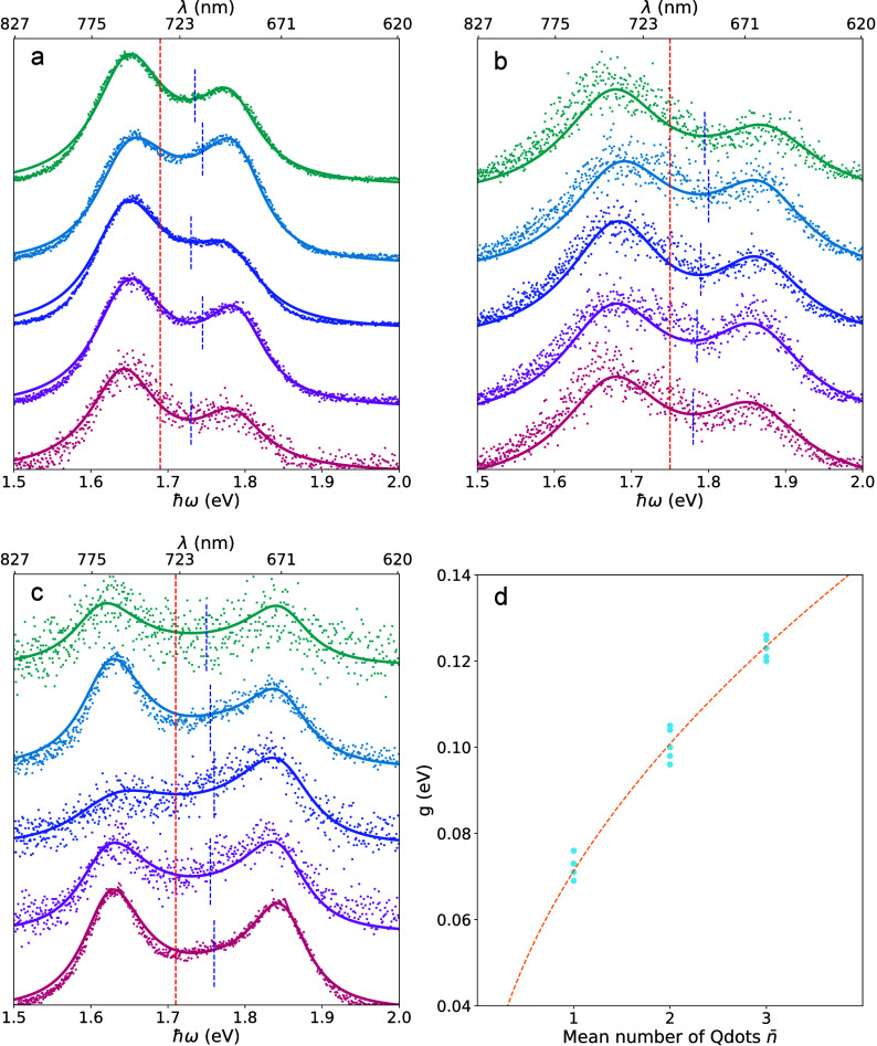 4
4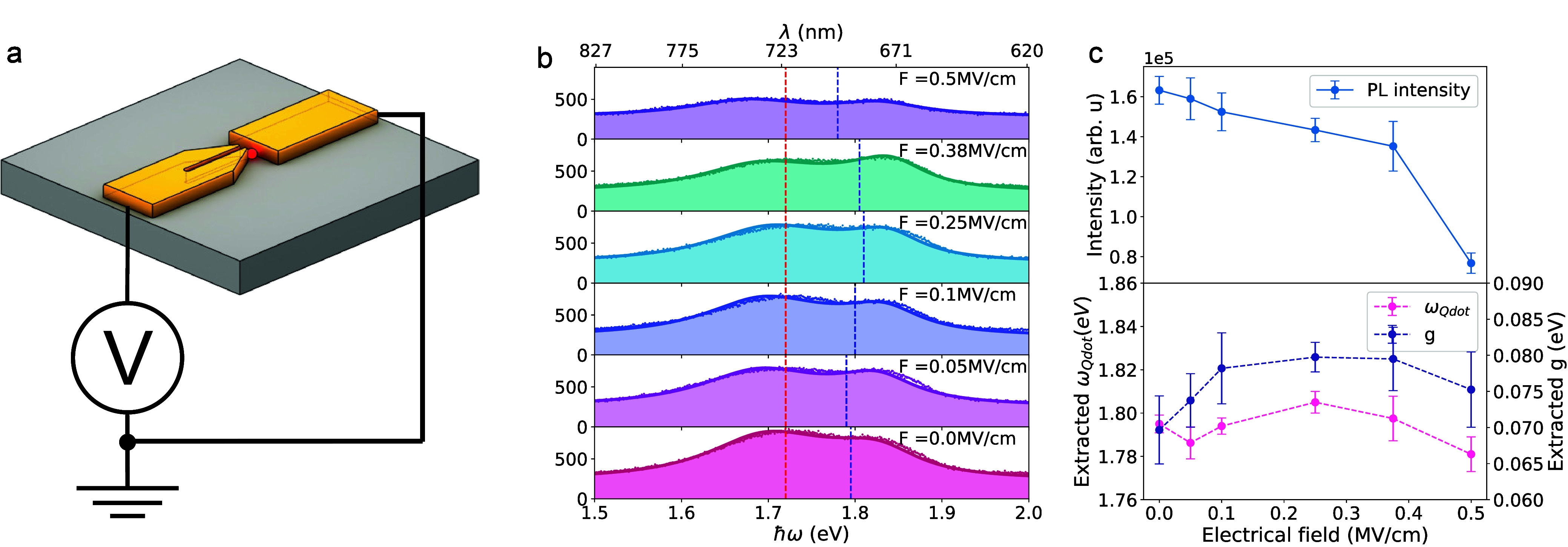 5
5- —H2020 Future and Emerging Technologies10.13039/100010664
- —Deutsche Forschungsgemeinschaft10.13039/501100001659
- —Deutsche Forschungsgemeinschaft10.13039/501100001659
- —Deutsche Forschungsgemeinschaft10.13039/501100001659
- —Deutsche Forschungsgemeinschaft10.13039/501100001659
- —Narodowe Centrum Nauki10.13039/501100004281
- —Bayerisches Staatsministerium f?r Wissenschaft und Kunst10.13039/501100021711
- —Research IrelandNA
Peer Reviews
No public reviews on file for this paper yet. If you reviewed it on a platform where reviews are public (OpenReview, ICLR, NeurIPS, ICML), you can paste yours below so the community can read it here.
Videos
No videos yet. Explain this paper in a talk, walkthrough, or lecture? Add one.
Taxonomy
TopicsPlasmonic and Surface Plasmon Research · Gold and Silver Nanoparticles Synthesis and Applications · Photonic Crystals and Applications
The spontaneous emission of a quantum emitter can be significantly modified by the local density of optical states when coupled to a resonant optical mode, leading to rich light–matter interaction phenomena, such as Purcell-enhanced photon emission. ?−? ? ? ? ? When the emitter and cavity are in the strong coupling regime, a new hybrid light–matter state, known as a polariton, emerges.? This state exhibits both photonic and excitonic characteristics and has enabled advances in areas such as Bose–Einstein condensation,? enhanced chemical reactivity,? and potentially modified superconductivity.?
Spectroscopically, strong coupling manifests as Rabi splitting in scattering, absorption, or photoluminescence (PL), indicating at least one complete cycle of coherent energy exchange between the emitter and the cavity. Achieving this regime requires a coupling strength g that exceeds both the cavity loss and emitter decay rates, including dephasing, which is especially challenging at room temperature. Dielectric cavities, with their high quality factors (Q), are advantageous in terms of small loss. ?,? However, to maximize the spectral overlap between such high-Q cavity resonances and quantum emitters, a cryogenic environment is typically required, as the emitter line width broadens with an increase in temperature. The line widths of the two coupled entities should be comparable to ensure sufficient spectral overlap, thereby maintaining the strong coupling condition.
In contrast, plasmonic cavities, consisting of nanoscale metallic structures, offer a deep subwavelength confinement of optical modes with moderate Q factors, yielding ultrafast energy transfer. This makes them promising candidates for achieving strong coupling at room temperature. However, realizing strong coupling in such systems demands precise spatial and spectral matching between the quantum emitter and the plasmonic cavity. In particular, optimal spatial matching poses a major challenge due to the need for nanometer-scale positioning of the emitter within the localized plasmonic field. Recent advancements have demonstrated various platforms and techniques to achieve strong coupling between quantum emitters and plasmonic cavities at room temperature, including particle-on-mirror structures, ?−? ? ? plasmonic tips, ?,? scanning slit cavities, ?,? bowtie antennas, ?−? ? and nanoparticles. ?−? ? ? Methods such as scanning probes ?,? or our own approach of integrating a slit cavity into an AFM tip ?,? offer additional flexibility by leveraging the nanometer-scale precision of AFM scanners, yet such devices are inherently serial and not easily scalable. Particle-on-mirror structures, on the other hand, provide extremely small mode volumes through self-assembled junctions. ?,? However, most implementations rely on drop-casting techniques, ?−? ? ?,?−? ? where quantum emitters are randomly deposited onto the plasmonic structures, resulting in nondeterministic placement and challenges in characterization. Moreover, while multistack architectures have been proposed for building devices, ?,? a planarized design is more favorable for integration with nanocircuitry or ultracompact nanophotonic platforms, particularly when additional elements can be incorporated into the strongly coupled system to enable extended functionality, such as integration with waveguiding and grating structures. Despite the progress of these approaches, fully on-chip integration remains highly desirable because it combines robustness, scalability, and compatibility with established top-down nanofabrication methods, offering a clear pathway toward ultracompact quantum photonic devices.
Here, we develop an on-chip plasmonic platform consisting of a slit-cavity structure and a counter electrode, as illustrated in Figurea. This open architecture allows retrofitting with a variety of quantum emitters and, in principle, can be integrated with additional waveguides. In this sense, it serves as a prototypical structure for devices whose functionality is based on cavity quantum electrodynamic effects, particularly strong coupling. Using a dielectrophoresis (DEP) process, one or several quantum emitters can be positioned near the tip of the slit, where the localized plasmonic-cavity mode exhibits a pronounced field maximum. Split PL spectra can be observed, indicating strong coupling. We find that the Rabi splitting strength varies between devices, which we attribute to differences in the number of quantum emitters coupled to the cavity mode. Additionally, we attempt to tune the emitter resonance via the quantum-confined Stark effect (QCSE) by applying an external voltage. However, due to significant spectral diffusion of the emitters at room temperature, the tunability can barely be observed with a typical decrease in PL intensity. Our experiments demonstrate on-demand strong coupling at room temperature in an ultracompact on-chip plasmonic device, highlighting its strong potential for integration into quantum photonic circuits.
Plasmonic Slit-Cavity Characterization
On-chip plasmonic slit-cavity structures are fabricated using monocrystalline gold flakes with a thickness of 40 nm, employing helium ion milling (see the scanning electron microscopy (SEM) image and inset of Figureb). The primary motivation for using solution-synthesized Au flakes in this work is their single-crystalline nature and ultrasmooth surface, which are difficult to achieve using standard evaporated Au films. Single-crystal Au flakes significantly reduce grain-boundary scattering and surface roughness, both of which are critical for achieving reproducible plasmonic resonances and strong field confinement in sub-10 nm slit cavities. These properties are particularly important for observing strong coupling at room temperature and for ruling out spurious spectral features arising from structural inhomogeneities. The nanoscale resolution and robustness of this fabrication method enable the on-demand creation of individual well-defined structures with high reproducibility. The slit cavity supports Fabry–Pérot (FP) modes, which depend on the slit’s length and width. As demonstrated in Figurec, using quasi-normal mode analysis (section S1 of the Supporting Information), the resonance of second- and third-order FP modes, characterized by the number of field maxima in the slit (Figured), can be tuned by varying the slit length while keeping the width fixed. Besides, we also find that the free spectral range of the FP modes is sufficiently large to allow only a single FP mode to couple with the quantum emitter. Furthermore, the second- and third-order FP modes exhibit quadrupolar-like field distributions (Figured), which helps to suppress radiation losses and therefore yield a relatively high Q.
In our experiment, we chose a slit length of 215 nm and a width of 7 nm to match the resonance of the quantum emitter. The slit width is comparable to the size of the emitter, enabling an effective spatial overlap of the mode emanating at the tip and the quantum emitter. An additional counter electrode is fabricated opposing the tip of the slit cavity with a gap of approximately 20 nm. This adds great versatility to the platform. For example, AC and DC voltages can be applied across the gap, allowing for dielectrophoresis and to induce Stark shifts in emitters. The resulting FP mode in the plasmonic slit cavity is verified through photoluminescence (PL) spectroscopy under high excitation intensity, allowing both spatial and spectral characterization.
To record spatially resolved PL spectra of the device shown in Figureb, we use hyperspectral imaging with the experimental setup depicted in Figure S2. Figuree shows a hyperspectral map collected by scanning the excitation spot across the entire device area. A bright localized spot appears at the plasmonic slit-cavity position when the signal is integrated over the spectral range of its resonance. The corresponding PL spectrum recorded at the brightest spot is shown in Figuref, where a shoulder on the broad gold PL background indicates the slit-cavity mode resonance. By applying a cumulative fit, we extract a cavity resonance at 1.71 eV with a quality factor Q of 15.6 (section S2).
Quantum Emitter Characterization
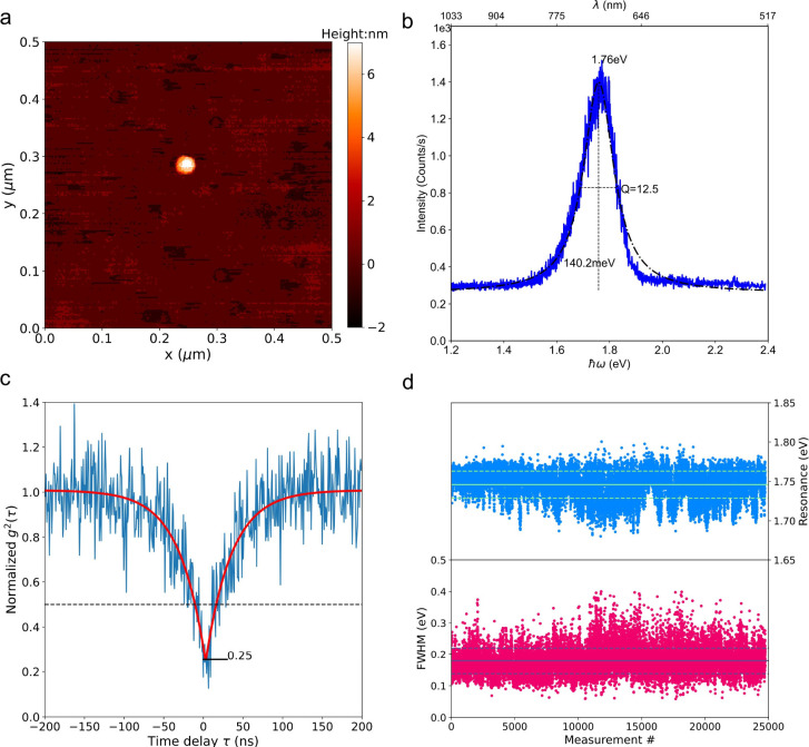
The quantum emitters used in our experiments are commercial colloidal core–shell quantum dots (Qdots, 705 nm, CdSeTe/ZnS, Thermo Fisher). These Qdots are first spin-coated onto a clean coverslip to characterize their physical and optical properties. The atomic force microscopy (AFM) image in Figurea shows a typical single Qdot exhibiting an apparent diameter of approximately 15 nm and a height of approximately 7 nm, which closely matches the width of the slit cavity. The Qdot’s emission spectrum, excited by a green laser, is displayed in Figureb. It can be fitted with a Lorentzian profile, yielding a resonance energy of 1.76 eV and a relatively broad emission line width of 140 meV. Single-photon emission by individual Qdots is confirmed by intensity autocorrelation measurements, as depicted in Figurec. Clear antibunching behavior is observed with a dip down to 0.25 at zero time delay. The corresponding uncertainty analysis is presented in Figure S4b. Under ambient conditions, some Qdots are chemically unstable and prone to oxidation when exposed to laser excitation resulting, e.g., in a resonance shift.? To verify the absence of such behavior, we record time-traced PL spectra and extract the resonance energies and line widths using Lorentzian fitting, as shown in Figured and Figure S3. The data show no significant spectral shifts (i.e., no consistent blue- or red-shift), but we do observe substantial spectral diffusion at room temperature with spectral variations as large as 50 meV.
Characterization of single Qdots. (a) AFM image of a representative single Qdot, spin-coated on a glass coverslip. (b) PL emission spectrum (blue line) under green laser excitation with a power of 1 μW (intensity of 8.8 × 10⁶ W/m2). The spectrum is fitted with a Lorentzian function (black dotted–dashed line) to extract the resonance energy and line width. (c) Photon statistics of the Qdot emission measured by second-order autocorrelation. A clear antibunching dip down to 0.25 at zero-time delay confirms single-photon emission behavior. The corresponding uncertainty analysis is presented in Figure S4b. (d) Time-dependent PL spectra of a single Qdot (Figure S3), recorded with a temporal resolution of 33 ms. Resonance energies (blue dots) and line widths (red dots) are extracted from Lorentzian fitting. The average value and one standard deviation are indicated by solid and dashed lines, respectively.
DEP Process
To achieve strong coupling, one of the main challenges is positioning the quantum emitter with nanometer-scale precision to ensure spatial alignment with the localized-cavity mode. To overcome this problem, we employ a DEP process with a real-time feedback mechanism to attract and position single or multiple Qdots at the tip of the slit cavity, where the cavity mode’s plasmon-mediated electric field is also concentrated.? Prior to the DEP process, the Qdot solution is diluted in pure water at an appropriate ratio (1:10000). A 5 μL droplet of this diluted solution is then deposited onto the surface of the on-chip device. An alternating voltage is applied to the electrode containing the slit cavity, while the counter electrode is grounded (Figurea). This generates a nonuniform electric field that polarizes the quantum dots in solution, producing a net force that can either attract the Qdots toward or repel them from the slit tip, depending on the applied frequency (section S4). By carefully tuning the applied voltage and frequency, we can make the net force attractive, drawing nearby Qdots toward the slit tip, where the electric field gradient is strongest.
DEP process. (a) Schematic illustration of the setup used for DEP. A droplet of the Qdot solution (diluted 1:10000 with pure water) is placed on top of the device, and an AC voltage (amplitude, 2 V; frequency, 2 MHz) is applied across the plasmonic nanoslit cavity (left) and the grounded counter electrode (right). Under the influence of the nonuniform electric field, for the right range of frequencies, Qdots experience a dielectrophoretic force and migrate toward the tip of the slit cavity, where the field gradient is maximal. (b) Illustration of the resulting coupled structure after DEP. A Qdot (represented by the red sphere) is positioned at the end of the slit cavity. The inset shows a magnified image. (c and d) Real-time feedback mechanism based on PL signals detected by an APD, while scanning the focused excitation laser (power: 1 μW; intensity: 8.8 × 10⁶ W/m2) over the device. (c) Prior to DEP, no confined PL spot is observed. Dark regions correspond to the gold surface, and the brighter areas correspond to the weak autofluorescence of the cover glass. Also, at these positions, more excitation light is transmitted and possibly excites Qdots suspended in the solution, adding to background signals. (d) Once a Qdot is captured at the slit tip, a bright and localized PL spot appears. Scale bar: 1 μm. Panels c and d share the same color bar clearly showing an increased fluorescence at the tip apex between the electrodes. (e and f) AFM scans of two representative devices after the DEP process. (e) Single Qdot positioned at the cavity tip using DEP parameters: voltage of 2 V, frequency of 2 MHz, and duration of 3 s. (f) With modified DEP parameters (voltage of 2 V, frequency of 0.5 MHz, and duration of 3 s), a larger number of particles, possibly including contaminants, accumulate around the cavity tip. Scale bar: 500 nm.
To ensure successful placement of Qdots within the region of interest, we implement real-time feedback based on PL detection by using a high-bandwidth avalanche photodiode (APD). Before initiating the DEP process, we scan the excitation laser (532 nm, 1 μW) over the sample and record the resulting PL map (Figurec). From this map, the approximate position of the slit cavity can be identified, as indicated by the white dashed line. During DEP, the region of interest (slit cavity) is continuously monitored at a repetition rate of 100 Hz. As soon as Qdots are trapped at the cavity tip, a sharp increase in PL intensity is observed at that location (Figured), signaling the successful placement of Qdots. At this point, the DEP process is interrupted, and the device is allowed to dry for several minutes. The Qdots remained anchored at the desired location, as shown in Figureb. More details about the DEP process, its optimization, and parameters used can be found in section S4.
The resulting coupled structures are first characterized using AFM. By varying the DEP parameters, such as applied frequency and voltages, we can achieve different numbers of captured Qdots. In Figuree, it appears that only a single Qdot is attracted; however, this observation is not conclusive, as multiple Qdots could be stacked vertically, which cannot be resolved by AFM. Additionally, the DEP process attracts not only Qdots but also sometimes contaminants, as observed in Figuref.
Strongly Coupled Spectra in PL
Split PL spectra indicating strong coupling can be measured directly after the coupled structures are formed, as described above. Many experiments rely on observing split scattering spectra as evidence of strong coupling; however, such features can also arise from alternative mechanisms such as Fano resonances ?,? or inhomogeneous dielectric environments,? making the interpretation ambiguous. In contrast, split PL spectra, when combined with careful analysis of the uncoupled states, provide more definitive evidence of strong coupling. Typically, we focus a green excitation laser (power of 1 μW) on a position that simultaneously covers both the plasmonic slit cavity and Qdots, ensuring that the Qdots are primarily excited. To identify the correct position, we recorded a hyperspectral image and located the brightest spot by integrating over the spectral range of the Qdot emission. Notably, PL signals from the bare plasmonic slit cavity can be detected only under high excitation power (500 μW), and thus, they are negligible under our low-power conditions for strongly coupling experiments.
Once the Qdots are strongly coupled to the slit cavity, polaritons are formed through coherent energy exchange between excitons and cavity plasmons. This interaction manifests spectrally as a characteristic double-peak feature in the PL spectra, as shown in Figurea–c, recorded from three different devices prepared in separate experiments under the same conditions.
Split PL spectra recorded from different coupled structures. (a–c) Split PL spectra (dots) recorded from three different coupled structures and the corresponding fit (solid lines) of the quantum model. For each structure, five spectra were recorded with different integration times to verify its reproducibility and to elucidate the influences of spectral diffusion. Before the coupled structures were fabricated, the resonance of the slit cavity is characterized by PL with high power. The resonance frequency is marked by a red dashed line. The Qdot’s resonance is labeled by a blue dashed line, which is not fixed in the fitting to accommodate small but finite spectral diffusion at room temperature. The fitting parameters can be found in Tables S1–S3, respectively. (d) Extracted coupling strengths from three different structures are indicated by the dots. The orange line represents the corresponding comparison to theory assuming multiple emitters (indicated by n̅) coupled to a single cavity.
To interpret the experimental results, we use the Jaynes–Cummings Hamiltonian to model the interaction between a single plasmonic nanocavity mode and a two-level quantum emitter.? Lindblad terms are incorporated into the master equation to account for incoherent pumping and all relevant loss and dephasing channels (section S6). Because each experiment begins with a characterization of the slit cavity, cavity resonance frequency ω_cav_ and loss rate γ_cav_ can be accurately determined and fixed in the model. In contrast, Qdot emission frequency ω_qd_ and line width γ_qd_ are significantly affected by spectral diffusion at room temperature (Figured). These parameters are therefore adjusted slightly to fit the measured spectra (section S7).
Figurea presents five PL spectra acquired with different integration times along with theoretical fits using the quantum model. Variation of the integration time can provide insights into the effects of spectral diffusion. From the fits, an average coupling strength (g) of 72.4 ± 2.3 meV is extracted, which clearly satisfies the strong-coupling criterion: 2g > (γ_cav_ + γ_qd_)/2. Meanwhile, when the integration time varies from 33 ms to 1 s, the splitting feature remains clearly visible, with the Rabi splitting strength nearly unchanged.
The same fitting approach is applied to data sets recorded for different structures (Figureb,c), fabricated using identical procedures. The extracted coupling strengths are 101.4 ± 1.8 and 123.0 ± 2.3 meV, respectively. These variations in different coupled structures are likely to arise from different numbers of Qdots coupling to the same slit-cavity mode, with the effective coupling strength expected to scale as √ in Figured, in agreement with the Tavis–Cummings model.? This interpretation is supported by the fact that, in the Qdot aqueous solution, some emitters are present in the form of clusters, which can be verified by AFM scans of spin-coated Qdots on the coverslip in Figure S5 (Supporting Information S3). Additional results from other devices are presented in Figure S8d, where fluctuations in coupling strength can be ascribed to variations in the dipole orientation of individual Qdots. Furthermore, finite-difference time-domain (FDTD) simulations (Figure S7) provide an estimate of the single-emitter coupling strength of 72.8 meV, based on the calculated effective mode volume and the effective dipole moment of a Qdot. In our experiments, we did not observe coupling strengths exceeding those reported here. The reason for this is likely the extent of the spatially confined mode at the nanoslit-cavity tip, where the available mode volume restricts the number of Qdots that can couple strongly. Generally, the Qdot’s number can be measured via resolving the antibunching dip in photon statistic measurement. However, performing photon statistics measurements directly on cavity-coupled Qdots is considerably more challenging. After coupling, the polaritonic PL signal is intrinsically weak and accompanied by significant background contributions, which severely limits the signal-to-noise ratio. In addition, in the strongly coupled plasmonic system, the polariton lifetime is dramatically reduced and is expected to lie in the tens of femtoseconds regime due to the ultrafast decay of plasmonic modes (section S8). Resolving such rapid dynamics in conventional photon-correlation experiments is practically impossible, as the temporal resolution of standard single-photon counting setups is limited to hundreds of picoseconds. This limitation arises from the intrinsic timing jitter of photodetectors and their associated electronics. Consequently, any antibunching dip in the photon statistics would be narrower than the shortest possible time bin and therefore unresolvable. Recently, advances in ultrafast two-dimensional electronic spectroscopy have demonstrated significant potential for resolving the dynamics of coherent polaritonic states. ?,?
A key advantage of our on-chip platform is the ability to deterministically characterize each slit cavity prior to coupling experiments, something not feasible with systems such as bowtie antennas or particle-on-mirror structures. This pre-characterization eliminates uncertainties due to multiple-plasmonic mode interference and enables accurate estimation of coupling strength without uncertainties due to possibly large detunings or uncoupled entities. In the future, our on-chip platform can be further integrated with optical waveguides to form functional nanocircuitry. However, waveguides fabricated from pure gold typically exhibit high propagation losses, which limit their suitability for long-distance optical routing. To address this limitation, we have recently developed Au–Ag alloy structures that combine the lower optical damping of silver with the improved chemical stability of gold, offering a potential route to extend the effective propagation length of plasmonic waveguides.? In this scenario, CMOS-compatible metal deposition techniques with improved surface quality and reduced optical damping can be employed to enable scalable manufacturing. In addition, several established hybrid approaches enable efficient coupling between plasmonic nanoantennas or cavities and small-loss dielectric waveguides (e.g., Si, SiN, or TiN) through near-field or evanescent coupling over submicrometer distances. In such architectures, the plasmonic slit cavity serves as a highly localized light–matter interaction region, while optical routing is handled by adjacent dielectric components.
Electrically Connected Strongly Coupled Device
Benefiting from the electrically connected structure and the gap between the counter electrode and the slit tip, we leverage the quantum-confined Stark effect (QCSE) to deliberately tune the resonance of the trapped Qdot by applying a strong external electric field, as illustrated in Figurea. QCSE is a well-known phenomenon whereby increasing the electric field reduces the overlap between the electron and hole wave functions, resulting in a decreased PL intensity and a spectral shift. Typically, the linear and quadratic dependence on the electric field is sufficient to describe frequency shifts as?
where μ and α are the permanent dipole moment and polarizability of the Qdot, respectively, and E is the electric field acting on the Qdot, consisting of two contributions: E int, the internal electric field arising from the Qdot’s charged state (randomly oriented, e.g., through the addition or removal of a surface electron), and E applied, the externally applied electric field.
Electrically connected on-chip strong coupling devices. (a) Schematic illustration of the electrically connected on-chip strong coupling device. A DC voltage source is connected to the two electrodes after the coupled structure is formed. (b) Measured split PL spectra (dots) and corresponding fits from the quantum model (solid lines) under varying applied electric fields from 0 to 0.5 MV/cm. The red dashed line indicates the cavity resonance characterized prior to the DEP process, while the blue dashed line marks the Qdot resonance extracted from the fit. (c) Statistical analysis of PL intensities, extracted Qdot resonances, and coupling strength g across multiple spectra under different applied voltages. The PL intensity is calculated by integrating the total counts across the full spectral range.
In Figureb, we present PL spectra characteristic of strong coupling of a single Qdot to a plasmonic nanoslit cavity (Figurea) recorded under different applied DC voltages. When no voltage is applied, the extracted coupling strength is the same as that shown in Figurea for an average emitter number n̅ = 1. As the applied field strength increases, a clear decrease in PL intensity is observed. However, a significant and consistent shift in the Qdot resonance energy is not observed. To further investigate this, we analyze multiple split PL spectra under varying applied voltages and extract both the overall PL intensity and the Qdot resonance energy from the spectra, as shown in Figurec. While the PL intensity consistently decreases with an increase in E applied, the resonance shift exhibits no clear dependence on the electric field, with an overall tuning range of approximately 20 meV, still within the typical range of spectral diffusion. Notably, similar fluctuations in the Qdot resonance are also observed in the absence of an applied voltage, as shown in Figurea–c. Similar observations are presented in section S9 and Figure S9a,b, where alternating voltages were applied to the hybrid structures. Once again, the resonance shifts show no clear dependence on the applied voltage.
The Qdot resonance shift induced by the QCSE is typically within 20 meV, ?,?−? ? consistent with the shifts observed in Figurec. However, spectral diffusion driven by fluctuations in the local electric field can span up to 50 meV, making it difficult to clearly resolve the QCSE-induced shift. This limitation could be addressed by using higher-quality Qdots with reduced spectral diffusion at room temperature or by applying higher electric fields to enhance the Stark shift beyond the diffusion range. The latter approach, however, is technically challenging as the structures become increasingly vulnerable to damage under stronger electric fields. Another possible approach to address this issue is to perform similar measurements under cryogenic conditions, which would substantially suppress phonon-related broadening and environmental charge fluctuations, leading to reduced spectral diffusion and improved visibility of QCSE tuning. However, an important consideration arises under cryogenic operation. While the QD line width is expected to narrow due to reduced phonon interactions and spectral diffusion, the line width of the plasmonic cavity is comparatively insensitive to temperature. This disparity can reduce the spectral overlap between the QD emission and the plasmonic-cavity mode, which may, in turn, decrease the effective light–matter coupling strength. Therefore, cryogenic operation alone does not provide a straightforward solution to this limitation.
In summary, we demonstrate an on-chip platform for achieving strong light–matter interaction between single or a few Qdots and a plasmonic slit cavity. Precise spatial positioning of Qdots at the cavity hot spot is realized using a DEP process integrated with real-time PL feedback. The coupled structures exhibit clear spectral splitting in PL, consistent with predictions of a quantum model assuming coupling of a two-level system with a single mode. By precharacterizing the plasmonic-cavity properties, we reliably extract coupling strengths for a multitude of fabricated devices. Our analysis reveals variations in coupling strength across different hybrid structures, which are likely determined by the number of emitters coupled to the cavity mode. Furthermore, we explore electrical control over the Qdot resonance via QCSE enabled by the integrated electrodes of the lateral device architecture. While applied electric fields modulate the PL intensity, spectral diffusion at room temperature obscures clear observation of Stark shifts. These results highlight the potential of deterministic, ultracompact, and electrically tunable quantum plasmonic systems for applications in quantum information processing, tunable photonic devices, and an integrable on-chip quantum light source.
Methods
Sample Preparation
Monocrystalline gold flakes are synthesized in solution following established protocols. ?−? ? Flakes with a suitable thicknesses are selected based on transmission measurements and transferred onto a substrate prepatterned with gold electrodes using a standard optical lift-off process (Figure S1a). A gallium-focused ion beam (Ga-FIB) is then used to isolate individual electrodes and define a large optical window along with coarse structural features (Figure S1b). High-precision slit cavities and tip gaps are subsequently fabricated using helium ion milling (Orion nanoFab, Zeiss).
Commercial colloidal semiconductor quantum dots (CdSeTe/ZnS Qdot 705 ITK Carboxyl, Q21361MP, Thermo Fisher Scientific) are used as quantum emitters in our experiments. The Qdot solution is diluted in Milli-Q water to achieve appropriate concentrations for different measurements. The aqueous solution was carefully prepared to ensure a uniform distribution of quantum dots across the glass coverslip, avoiding any interaction between different quantum dots. For basic characterization, a 1:6000 dilution is spin-coated onto cleaned microscope coverslips (Gerhard Menzel GmbH). For DEP positioning, a more dilute solution (1:10000) is used.
Optical Setup
The PL measurement setup is sketched in Figure S2. A 532 nm continuous wave laser (AIST-NT ROU006) serves as the excitation source and is focused onto the sample by using a high-numerical aperture objective (Nikon CFI P-Apo 100×, NA 1.45). For characterizing single-Qdot emission and conducting coupling experiments, an excitation power of 1 μW is typically used, while a higher power of 500 μW is applied to probe gold photoluminescence. The emitted PL signal passes through a dichroic mirror and is routed via a flip mirror either into a spectrometer (HORIBA iHR320) equipped with an EMCCD detector (Andor Newton 970p) or toward a time-resolved photon statistics setup. Independent piezoelectric stages control the sample mount and objective, enabling precise alignment of the laser focus with the sample. Time-correlated single-photon counting (TCSPC) measurements are performed by splitting the PL signal with a 50:50 beam splitter and detecting photons using two avalanche photodiodes (APDs, SPCM-AQR). Photon arrival times are recorded using a field-programmable gate array (FPGA, qutools quTAU H+).
Supplementary Material
The reference list from the paper itself. Each links out to its DOI / PubMed record.
- 1He Y.-M.He Y.Wei Y.-J.Wu D.Atatüre M.Schneider C.Höfling S.Kamp M.Lu C.-Y.Pan J.-W.On-Demand Semiconductor Single-Photon Source with near-Unity Indistinguishability Nature Nanotechnol.20138321321710.1038/nnano.2012.26223377455 · doi ↗ · pubmed ↗
- 2Purcell E. M.Torrey H. C.Pound R. V.Resonance Absorption by Nuclear Magnetic Moments in a Solid Physical review 1946691–23710.1103/Phys Rev.69.37 · doi ↗
- 3Goy P.Raimond J.Gross M.Haroche S.Observation of Cavity-Enhanced Single-Atom Spontaneous Emission Physical review letters 19835024190310.1103/Phys Rev Lett.50.1903 · doi ↗
- 4Badolato A.Hennessy K.Atature M.Dreiser J.Hu E.Petroff P. M.Imamoglu A.Deterministic Coupling of Single Quantum Dots to Single Nanocavity Modes Science 200530857251158116110.1126/science.110981515905398 · doi ↗ · pubmed ↗
- 5Akselrod G. M.Argyropoulos C.Hoang T. B.CiracìC.Fang C.Huang J.Smith D. R.Mikkelsen M. H.Probing the Mechanisms of Large Purcell Enhancement in Plasmonic Nanoantennas Nat. Photonics 201481183584010.1038/nphoton.2014.228 · doi ↗
- 6Hoang T. B.Akselrod G. M.Mikkelsen M. H.Ultrafast Room-Temperature Single Photon Emission from Quantum Dots Coupled to Plasmonic Nanocavities Nano Lett.201616127027510.1021/acs.nanolett.5b 0372426606001 · doi ↗ · pubmed ↗
- 7Rivera N.Kaminer I.Light–Matter Interactions with Photonic Quasiparticles Nature Reviews Physics 202021053856110.1038/s 42254-020-0224-2 · doi ↗
- 8Deng H.Haug H.Yamamoto Y.Exciton-Polariton Bose–Einstein Condensation Rev. Mod. Phys.20108221489153710.1103/Rev Mod Phys.82.1489 · doi ↗