High-Frame-Rate Low-Noise Global Shutter CMOS Image Sensor for High-Speed Machine Vision
Abhinav Agarwal, Jatin Hansrani, Kazuhisa Suzuki, Karthik Venkatesan, Wilson Law, Varun Shah, Kai Ling Ong, Danny Marine, Oleksandr Rytov, Tim Lu, Neil Kumar, Edward Enriquez, Liviu Oniciuc, Sam Bagwell, Loc Truong, Anders Andersson, Radu Corlan

TL;DR
A new CMOS image sensor with high frame rates and low noise is developed for high-speed machine vision applications.
Contribution
A low-noise, high-frame-rate global shutter CMOS image sensor with UHD resolution is introduced for high-speed machine vision.
Findings
The sensor achieves 1141 FPS at 12 bits and 1694 FPS at 8 bits at full resolution.
It features a 5 µm global shutter pixel with dual-gain capability and low read noise.
The sensor streams video through 16 CML data ports at 7.44 Gbps each, achieving 119 Gbps throughput.
Abstract
In this paper we present a low-noise, high-frame-rate global shutter CMOS image sensor with UHD resolution (3840 × 2160), targeting high-speed machine vision applications. The sensor (ForzaFAST581) supports video capture at up to 1141 FPS at 12 bits and 1694 FPS at 8 bits at full resolution, consuming a total power of 5.5 W. Fabricated in a 65 nm, four-metal BSI process, the imager features a 5 µm voltage-domain global shutter pixel with dual-gain capability for improved dynamic range and a read noise of 3.04 e− in global shutter and 2.15 e− in rolling shutter mode for high-gain at maximum frame rate operation. For compact camera integration and low power consumption, the sensor is designed to stream video through 16 CML data ports, each operating at 7.44 Gbps, achieving a total aggregate throughput of 119 Gbps. Additionally, the sensor supports selectable output bit depths—8-bit,…
Genes, proteins, chemicals, diseases, species, mutations and cell lines named across the full text — each resolved to its canonical identifier and authoritative record.
Click any figure to enlarge with its caption.
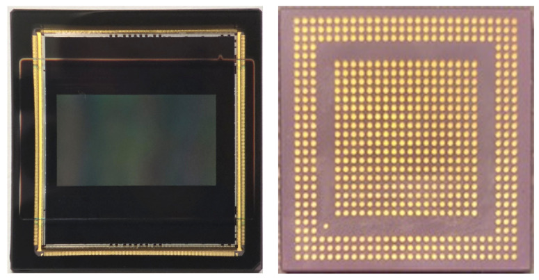 Figure 1
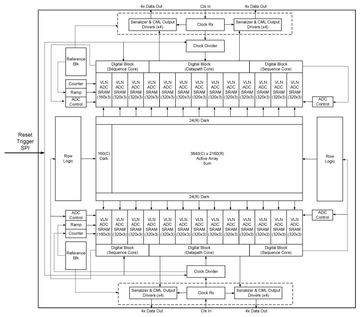 Figure 2
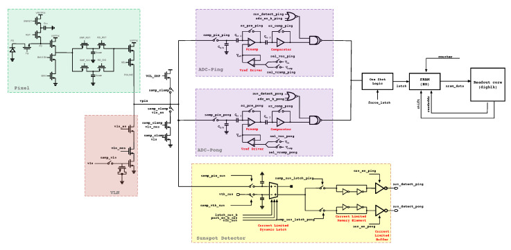 Figure 3
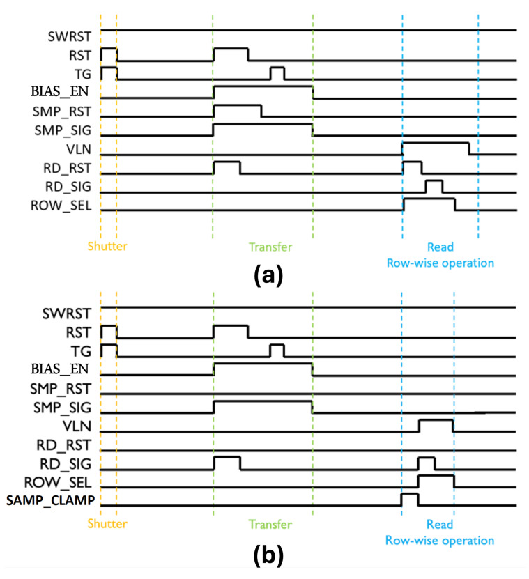 Figure 4
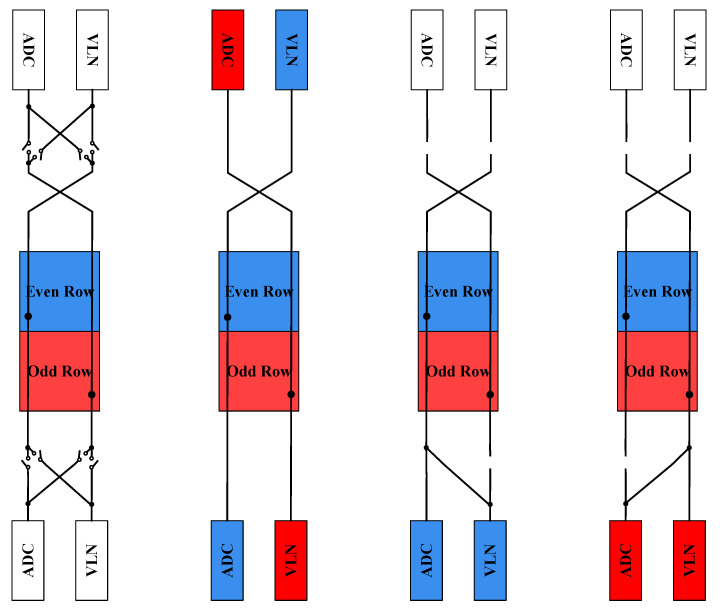 Figure 5
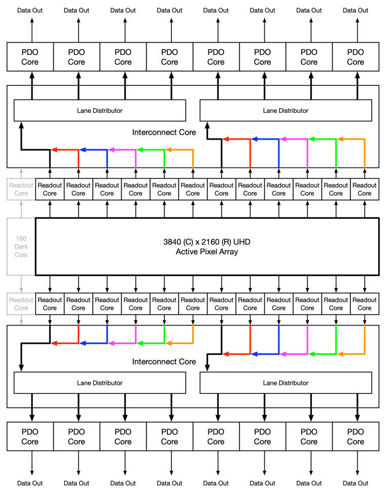 Figure 6
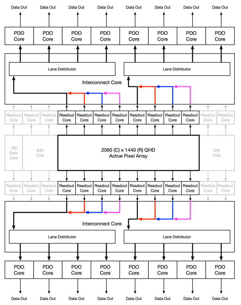 Figure 7
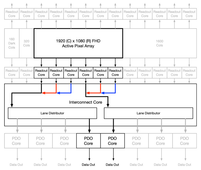 Figure 8
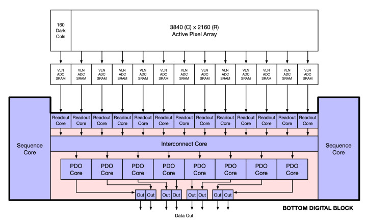 Figure 9
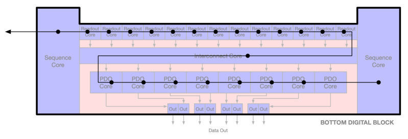 Figure 10
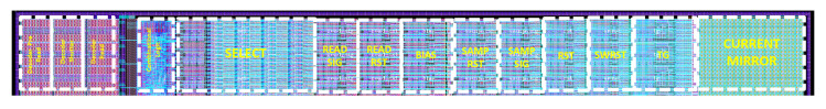 Figure 11
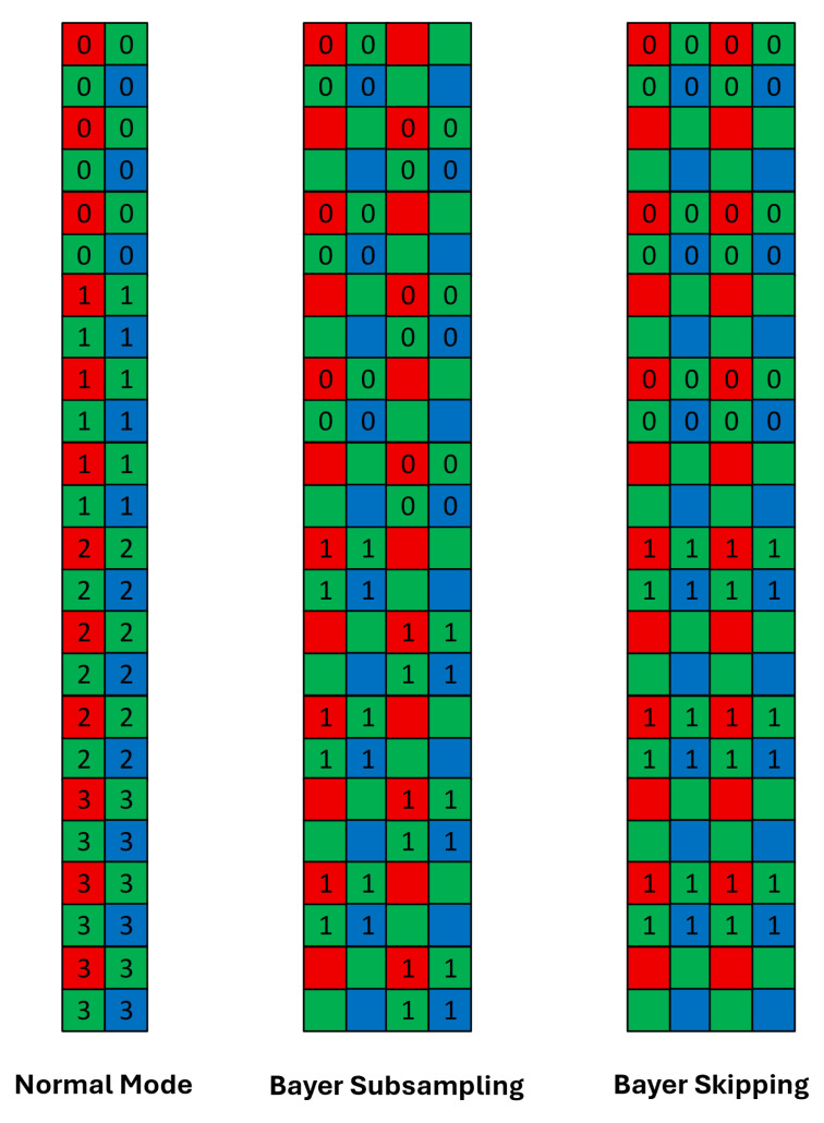 Figure 12
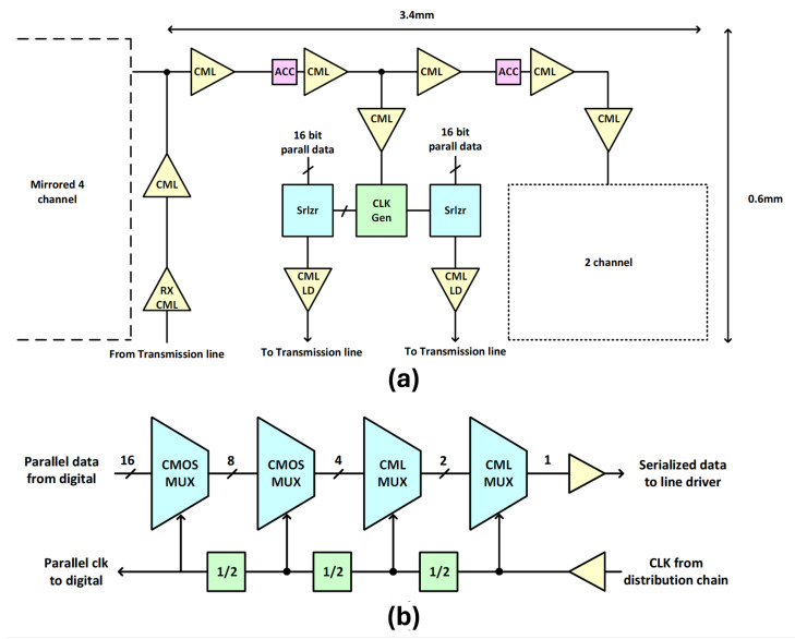 Figure 13
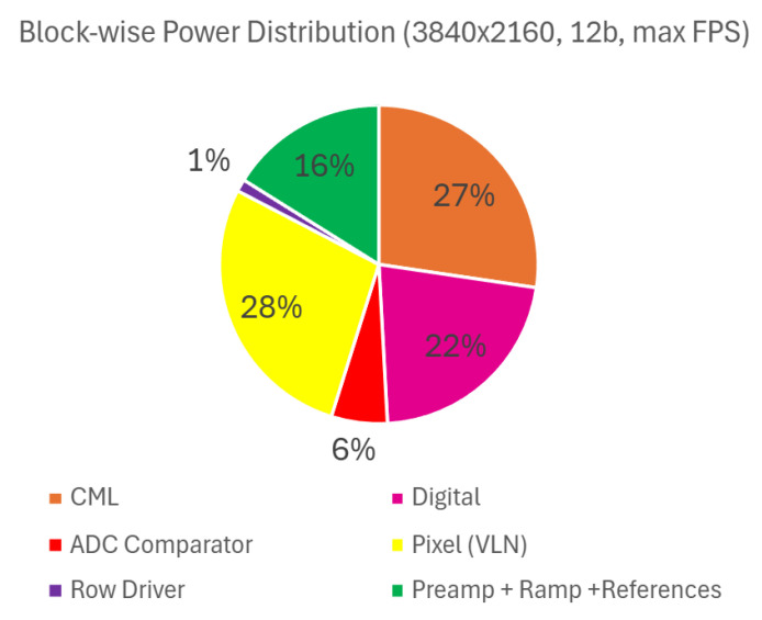 Figure 14
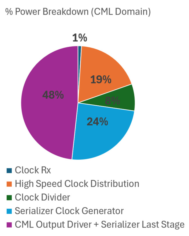 Figure 15
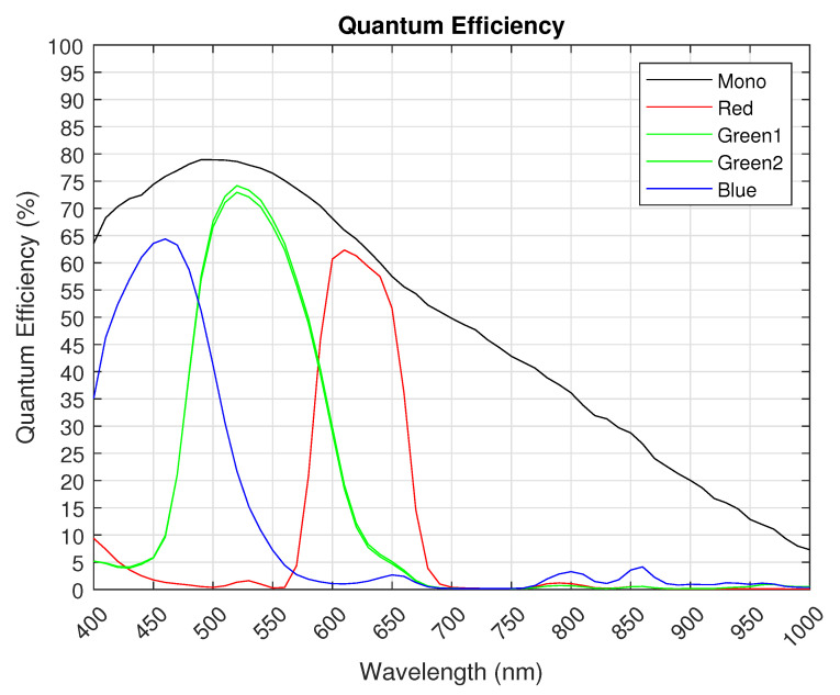 Figure 16
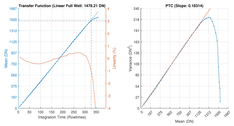 Figure 17
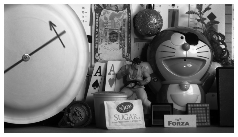 Figure 18
Peer Reviews
No public reviews on file for this paper yet. If you reviewed it on a platform where reviews are public (OpenReview, ICLR, NeurIPS, ICML), you can paste yours below so the community can read it here.
Videos
No videos yet. Explain this paper in a talk, walkthrough, or lecture? Add one.
Taxonomy
TopicsCCD and CMOS Imaging Sensors · Analog and Mixed-Signal Circuit Design · Advanced Optical Sensing Technologies
1. Introduction
High-speed machine vision systems are increasingly deployed in applications such as industrial inspection, automotive safety testing, advanced microscopy, and slow-motion sports analysis, where capturing fast-moving subjects with high temporal resolution and minimal distortion is essential. A key enabler of these systems is the image sensor. In particular, a high-frame-rate, low-noise, global shutter CMOS image sensor is critical for accurately capturing transient events without motion artifacts or rolling shutter distortions.
While traditional rolling shutter CMOS image sensors offer advantages such as lower temporal noise and simpler pixel architecture, they suffer from temporal skew and motion blur—limitations that reduce their effectiveness in scenes with rapid motion. In contrast, global shutter (GS) pixel architectures enable true snapshot imaging by simultaneously exposing all pixels, thus eliminating temporal distortion. However, these architectures [1,2,3,4,5,6,7] often introduce trade-offs, including increased dark temporal noise, reduced fill factor, and diminished dynamic range, primarily due to the added complexity and in-pixel storage elements required for global transfer operation.
Recent advancements in pixel design, low-noise analog front ends, and high-speed ADCs have significantly closed the performance gap between global and rolling shutter image sensors. These innovations now allow GS CMOS image sensors to retain their temporal advantages while achieving competitive image quality, thereby expanding their applicability in high-performance machine vision systems where both speed and image quality are critical.
In this work, we present a high-frame-rate, low-noise global shutter CMOS image sensor optimized for high-speed machine vision applications (Figure 1). The design focuses on maximizing output frame rate while maintaining image quality through low noise, minimized horizontal smearing, and support for short integration times (<2 µs) [8].
We have chosen a voltage-domain global shutter pixel architecture over a charge domain global shutter pixel architecture in this design primarily due to the requirement of better Parasitic Light Sensitivity (PLS) [9]. The availability of the high density trench capacitor in the chosen process [10] helps to significantly minimize the pixel kTC noise, achieving noise performance more close to a charge domain global shutter pixel.
To further enhance versatility, the sensor includes column and row windowing as well as port concentration modes, which enable data throughput through a reduced number of output ports. Multiple spatial subsampling modes, such as Bayer skipping and Bayer sub-sampling, are supported to increase frame rate at lower resolutions. The readout architecture is configurable for both correlated double sampling (CDS) and non-CDS modes, allowing applications to balance noise and speed, especially during windowed readout. The sensor also supports selectable output bit depths—8-bit, 10-bit, and 12-bit—enabling additional optimization of frame rate based on application-specific requirements.
The remainder of the paper is organized as follows. Section 2 and Section 3 describe the sensor readout architecture and the row-logic implementation, respectively. Section 4 presents the high-speed SerDes architecture used for off-chip data transmission. Section 5 concludes the paper with a summary of the silicon measurement results.
2. Readout Architecture
The sensor block diagram (Figure 2) illustrates a top–bottom readout architecture in which six rows are read out concurrently. The pixel array readout is divided across two halves, with each side further partitioned into 12 superblocks, where each superblock reads 320 columns by 3 rows. The sensor employs a 12T voltage-domain global shutter pixel architecture with dual-gain capability. Within each pixel, two high-density deep trench capacitors (a cross-section of these deep trench capacitors is shown in [10]) store the reset and signal levels required for CDS readout. The capacitor sizes are carefully optimized to minimize kTC noise—a dominant component of overall pixel noise. A shared source follower configuration is used for pixel readout to suppress FPN and reduce the number of pixel output lines.
To enable high frame rates, the row time must be minimized; this is achieved using a ping-pong single-slope ADC architecture, which pipelines sampling and ADC conversion. Figure 3 illustrates the analog readout signal chain of the image sensor. The authors refer readers to one of our previous works [11], which provides a comprehensive discussion of the challenges associated with high-speed ping-pong ADC architectures, with particular emphasis on minimizing electrical crosstalk between ADC pairs and mitigating differential nonlinearity (DNL) arising from high-speed counter distribution networks. In addition, one of our company white papers [12] presents detailed techniques for modeling and reducing low-light integral nonlinearity (INL) effects in ping-pong ADC architectures.
In this implementation, the row time is primarily limited by the time required to sample both the reset and signal levels into the ADC during rolling readout. To trade off dark temporal noise for increased frame rate, a non-CDS readout mode is also supported, wherein a local ADC clamp can auto-zero the preamplifier and comparator—thereby reducing the reset sampling time. A high-level timing diagram illustrating pixel operation in CDS and non-CDS modes is shown in Figure 4. For the CDS timing, the read reset pulse during transfer phase is used to clear the residual charge on the parasitic capacitor at the gate of the output source follower. This helps to minimize any signal-dependent memory effect/lag on the next video frame. Please note that even though the pixel is inherently a dual gain pixel, we do not have a built-in dual gain mode implemented on-chip. The imager can either operate in high gain (SWRST always ON) or low gain (RST always ON) but not in interscenic or intrascenic dual gain mode.
To support concurrent readout of six rows, each pixel column includes six pixlines. By default, even-numbered pixlines connect to the bottom readout chain, while odd-numbered pixlines connect to the top chain. To enable both dual-sided and single-sided readout modes—useful for port concentration—dynamically programmable switches are inserted along the even and odd pixlines. These switches allow each pixline to be routed to the ADC or VLN (or both), depending on the selected configuration as illustrated in Figure 5.
In dual-sided readout, the VLN associated with a given pixline resides on the opposite side from its ADC. In contrast, during single-sided readout, the programmable switches enable all pixlines to access both the ADC and VLN from the same side of the readout chain. One half of the readout circuitry can be completely powered down, resulting in significant power savings.
Flexible readout modes allow the sensor to output data through eight different port configurations. Larger resolutions will generate more pixel data, which can be read out faster using more output ports. Smaller resolutions will generate less pixel data and can be configured to use fewer output ports to save on power. This flexibility affords the sensor a variety of applications. The readout configuration is a function of two parameters: the resolution and desired number of output ports. The resolution determines how many superblocks are to be read out, and the number of output ports determines how the pixel data should be distributed.
All superblocks operate in parallel, each acquiring 320 columns by 3 rows worth of data. Each superblock writes their data into buffers immediately after acquiring the pixel data, while reading out from these buffers is done serially. After one buffer is emptied, the read operation points to the next buffer. A read controller determines which buffer to start reading from, when to transition to the next buffer, and the read rate. Figure 6 illustrates the flow of the pixel data through the digital data path for a UHD resolution.
The flexibility in the read controller allows windowed ROIs to still make use of all output data ports. Figure 7 shows the flow of the pixel data when windowed to QHD resolution. The data read from these buffers are streamed into two data channels. Each channel runs in parallel and always starts reading from the left buffer first. As each set of data comes in, it is evenly distributed to up to four output ports. If fewer ports are desired, then the channel controller will adjust the distribution. Figure 8 shows an off-centered FHD frame, outputting to only 2 ports in single-sided readout.
Once the data has been distributed to the output ports, framing information and meta data will be inserted into the data stream. This completed data stream will then be transformed using 64b/66b encoding to provide statistical bounds on DC balance, bit transition density, and allow for clock recovery. Flexibility in the readout configuration (resolution, windowing ROI, output bit depth, number of ports) is one the key features of the sensor’s data path.
One of the challenges of the digital block design comes from the implementation limitations, physical dimensions, and limited number of metal layers. The image sensor height is predominately made up of the pixel array and the readout circuitry through the top and bottom sides, leaving less than 1 mm each for the digital block height. This is further exacerbated by the width being over 21 mm, resulting in a very long and narrow shape. This can increase routing congestion since many signals that have to travel between the two ends will inevitably limit how local signals can move horizontally.
In addition, various digital cores are implemented as macro blocks. This approach allows a single timing for the clean macro blocks to be arrayed out, while maintaining identical timing parameters. One downside is that the macros will block out any routing in the higher levels of hierarchy, keeping signals inside the macro strictly separate from signals outside of the macro. Many of the macros contain memory IP cores and so are limited in what kind of dimensions they can have. To address this limitation, certain digital control signals are routed through the macro blocks. This approach makes use of any available space in the macros but also eases the routing congestion outside. Figure 9 illustrates the connectivity between the different macros inside the digital block. The blue blocks represent macros, while the red areas depict the open space that can be used for routing and timing closure.
In Figure 9, the width of the readout cores and the interconnect core spanned nearly the full width of the digital block. The interconnect core was abutted to the sequence core meaning that there was no available path over or around the interconnect core. Anything passing between the readout core and the PDO cores had to first go through the interconnect core or the sequence cores. Certain interfaces, such as the digital test bus or communication bus, would have to snake through the digital block, as shown in Figure 10.
3. Row Logic
The row-logic block (Figure 11) integrates the row decoders, spatial sub-sampling control logic, pixel-control signal generators, and current-mirror biasing network. Three independent decoders are implemented to generate the pre-read, shutter, and read pointers required for supporting both global-shutter and rolling-shutter readout modes. The associated combinational logic is synthesized to provide the necessary control stimuli for multiple spatial sub-sampling modes, including Bayer skipping and Bayer sub-sampling providing up to 2× frame rate boost (Figure 12).
A significant portion of the layout area is occupied by the nine dedicated pixel-control generators, which produce the key timing signals for each row: reset (RST), overflow (SWRST), transfer gate (TG), bias-enable (BIASSEL), sample-reset (SMP RST), sample-signal (SMP SIG), read-reset (RD RST), read-signal (RD SIG), and row-select (ROW SEL). Each generator incorporates a latch-based control circuit followed by a current-limited driver to ensure consistent edge shaping and robust signal delivery across the array.
The block also includes a current-mirror subsystem formed by repurposed pixel cells arranged as a bias-generation network. This structure provides a nominal 150-nA bias current to each pixel in the array, ensuring uniform operating conditions and minimizing pixel-to-pixel variation.
4. High-Speed Interface Design
Operating at UHD resolution at high frame rates, the image sensor generates a substantial volume of data, necessitating careful design, simulation, and optimization of the entire high-speed signal chain. To ensure seamless integration into the final camera system, several product-level constraints—such as a compact form factor, a reduced number of FPGAs in the data downlink, and low-power operation—shaped the high-speed clock distribution and SerDes architecture. The number of high-speed data ports was limited to 16 to align with system-level FPGA constraints, making it critical to maximize data throughput per port. Additionally, implementation on a 65nm process node with only four metal layers imposed further limitations on routing resources, driving the need for precise impedance control and signal integrity optimization across the high-speed paths.
The high-speed signal chain comprises several key components, including the clock receiver, clock distribution network, serializer, and CML output driver (Figure 13a). A high-speed differential input clock operating at 3.72 GHz is supplied to both the top and bottom sides of the sensor readout. This clock is distributed through a high-speed CML-based clock distribution network to all eight CML output data ports—four located on the left and four on the right—ensuring synchronized data transmission across the entire high-speed interface.
To achieve UHD resolution at 12-bit depth and 1100 FPS, each of the 16 CML output ports (8 on the top and 8 on the bottom) operate at 7.44 Gbps. The clock receiver is a CML buffer comprising multiple amplification stages, designed to boost the small-swing differential input clock to a level sufficient for the clock distribution network. This receiver is placed at the center of a T-shaped clock tree, with each branch spanning 3.4 mm.
The number and placement of CML buffers along the clock distribution network are optimized through theoretical analysis—accounting for attenuation per unit trace length—and validated by post-layout simulations to ensure clock fidelity at each stage. A key challenge is common-mode imbalance in the differential clock, caused by random device mismatch and trace impedance variations. If uncorrected, this imbalance can degrade the differential signal, potentially leading to clock failure after several stages.
To mitigate this, AC coupling is introduced periodically in the clock path. While effective in restoring common-mode balance and filtering low-frequency noise from earlier stages, AC coupling introduces additional parasitic capacitance due to the coupling capacitor (realized using MOS devices) and the input capacitance of the CML stage. This imposes a practical limit on the number of AC coupling stages. The high-pass filter formed by the AC capacitor and bias resistor is designed with a cutoff frequency at one-fourth of the operating clock frequency. However, larger capacitors add parasitic loading, and higher-value resistors increase thermal noise, necessitating careful sizing trade-offs to balance signal integrity and noise performance.
To further minimize substrate-related uncertainties, additional metal shielding is routed beneath the high-speed signal traces to provide controlled coupling and reduce undesired coupling to the substrate. While layout extraction tools often model the substrate as a zero-impedance ground, in practice, it exhibits a distributed RC behavior that depends heavily on layout geometry and process parameters. To mitigate these effects, the thick top metal layer—available in the 4-metal process—is utilized for routing critical signals, thereby reducing resistance and parasitic capacitance. This approach helps maintain stable duty cycles, which is essential for robust DDR operation of the serializer.
As shown in Figure 13a,b, the clock generation block produces a divided clock for the 16:1 serializer, shared between two serializer units placed symmetrically on the left and right sides. High-speed clock domains utilize CML-type dividers, whereas CMOS TSPC-based dividers are employed for low-speed clock generation. In stages 1 and 2, the divided clock signals are converted to CMOS levels. The stage 1 clock is also used as a parallel clock routed to the digital block. This ensures synchronization between the digital parallel data and the serializer input.
The serializer is structured as a multi-stage multiplexer (MUX) tree optimized for both performance and area efficiency:
- CMOS Stages: The first stage consists of eight units of 2:1 CMOS MUXes implemented using TSPC logic for low-power, compact operation at low frequencies followed by the second stage with four units of 2:1 CMOS MUXes to further serialize data.
- CML Stages: The third stage has two units of 2:1 CML MUXes followed by the fourth stage consisting of just one unit of 2:1 CML MUX with a one-clock delayed data path generated to support post-emphasis functionality, which improves signal integrity at high data rates.
The serializer output connects to a CML output driver with a 50 Ω resistive load for impedance matching with the transmission line. An integrated post-emphasis circuit with programmable coefficients compensates for channel loss, enhancing high-frequency signal quality. To ensure robustness, reverse-biased diodes are placed at each differential output for ESD protection. Additionally, RLC elements are inserted in the supply and ground paths during post-layout simulations to model bonding wire effects. The transmission channel is characterized using S-parameter data to accurately capture high-speed behavior and guarantee signal integrity.
5. Results and Summary
Table 1 and Table 2 summarize the scaling of maximum achievable frame rates and power consumption for various standard video resolutions for different bit depths and various port configurations for the CDS and non-CDS modes, respectively. The sensor’s readout architecture is designed to support higher frame rates when operating at reduced resolution formats. Across the supported video formats and output-port configurations, the maximum achievable frame rate generally increases as the ADC bit-depth is reduced from 12-bit to 10-bit and further to 8-bit. For the UHD format, the frame rate is consistently constrained by the total available output bandwidth, regardless of bit-depth. In contrast, for lower-resolution formats, the limiting factor depends on both ADC bit-depth and the number of active output ports. At 12-bit resolution, the ADC conversion time—set by the counter speed—typically governs the maximum frame rate. At 10-bit and 8-bit resolutions, the reset and signal sampling phases dominate the row time and therefore become the primary bottleneck instead of ADC conversion.Additionally, when operating with fewer output ports, the reduced output bandwidth can become increasingly limiting as the video resolution increases. In such cases, bandwidth constraints may dominate over sampling and ADC-conversion limits, particularly for higher-resolution video modes.
A noticeable reduction in total power consumption is observed when fewer output data ports are used. In dual-sided readout mode, the savings primarily stem from disabling unused serializers and output drivers. In single-sided readout mode, additional power reduction is achieved by powering down the entire readout circuitry on the inactive side, including VLN, ADCs, SRAMs, digital logic, clock distribution, serializers, and output drivers. This selective shutdown of components contributes significantly to overall power efficiency. Figure 14 illustrates the relative contribution of major sub-blocks to the overall power consumption, presented as a percentage breakdown. Figure 15 shows the major contributors to the CML domain power consumption. To optimize power consumption for application-specific frame rate targets, the number of active output data ports can also be reduced without sacrificing performance.
Detailed specifications of the CIS sensor are presented in Table 3 along with QE curves for mono and RGGB CFA in Figure 16. The Photon Transfer Curve (PTC) and transfer function linearity are shown in Figure 17. A full-resolution 12-bit monochrome image captured at 1100 FPS is shown in Figure 18.
Table 4 presents a performance comparison of the proposed imager (ForzaFAST581) with other publicly available high-speed global shutter CIS devices of comparable UHD/4K resolution. While every effort has been made to align the specifications across sources, it should be noted that many manufacturers do not disclose complete parameter sets, and that some of the compared sensors may have been primarily designed for applications other than machine vision. The proposed imager demonstrates state-of-the-art performance in terms of noise and parasitic light sensitivity (PLS). In 12-bit mode, it achieves more than twice the frame rate of [13] while utilizing nine times fewer output ports, thereby enabling more compact camera integration, and provides an improvement of more than 14 dB in PLS. Relative to [14], the imager delivers over a twofold increase in frame rate (at 10-bit operation) together with approximately fifteen times lower noise. The proposed imager attains a slightly lower maximum frame rate than [15]; however, since no noise or linearity data are publicly available for that sensor, it remains unclear whether its higher frame rate is achieved at the expense of noise performance or overall image quality.
The reference list from the paper itself. Each links out to its DOI / PubMed record.
- 1Kumagai Y. Yoshita R. Osawa N. Ikeda H. Yamashita K. Abe T. Kudo S. Yamane J. Idekoba T. Noudo S. Back-Illuminated 2.74 µm-Pixel-Pitch Global Shutter CMOS Image Sensor with Charge-Domain Memory Achieving 10k e− Saturation Signal Proceedings of the IEEE IEDM San Francisco, CA, USA 1–5 December 2018237240
- 2Park G. Hsuing A.C. Mabuchi K. Yao J. Lin Z. Venezia V.C. Yu T. Yang Y.S. Dai T. Grant L.A. A 2.2 µm stacked back side illuminated voltage domain global shutter CMOS image sensor Proceedings of the 2019 IEEE International Electron Devices Meeting (IEDM)San Francisco, CA, USA 7–11 December 201916.4.116.4.4
- 3Cremers B. Freson T. Esquenet C. Vroom W. Prathipati A.K. Okcan B. Luypaert C. Jiang H. Witters H. Compiet J. A 5M Pixel Image Sensor with a 3.45 µm Dual Storage Global Shutter Back-Side Illuminated Pixel with 90 d B DR Proceedings of the 2023 International Image Sensors Workshop Crieff, UK 21–25 May 2023
- 4Kim S.S. Lee G.D. Park S.S. Shim H. Kim D.H. Choi M. Kim S. Park G. Oh S.J. Moon J. 3-Layer Stacked Voltage Domain Global Shutter CMOS Image Sensor with 1.8 µm-Pixel-Pitch Proceedings of the 2022 International Electron Devices Meeting (IEDM)San Francisco, CA, USA 3–7 December 202237.5.137.5.4
- 5Xu C. Mo Y. Ren G. Ma W. Wang X. Shi W. Hou J. Shao K. Wang H. Xiao P. 5.1 A stacked global-shutter CMOS imager with SC-type hybrid-GS Pixel and Self-Knee Point Calibration Single Frame HDR and On-Chip Binarization Algorithm for Smart Vision Applications Proceedings of the 2019 IEEE International Solid-State Circuits Conference-(ISSCC)San Francisco, CA, USA 17–21 February 20199496
- 6Lee J.K. Kim S.S. Baek I.G. Shim H. Kim T. Kim T. Kyoung J. Im D. Choi J. Cho K. 5.5 A 2.1 e− Temporal Noise and −105d B Parasitic Light Sensitivity Backside-Illuminated 2.3 µm-Pixel Voltage-Domain Global Shutter CMOS Image Sensor Using High-Capacity DRAM Capacitor Technology Proceedings of the 2020 IEEE International Solid-State Circuits Conference-(ISSCC)San Francisco, CA, USA 16–20 February 2020102104
- 7Isozaki T. Mori K. Miyauchi K. Yasuda N. Sawai Y. Tsai A. Takayanagi I. Nakamura J. Back Side Illuminated High Dynamic Range 4.0 μm Voltage Domain Global Shutter Pixel ITE Tech. Rep.20194358
- 8Agarwal A. Hansrani J. Suzuki K. Venkatesan K. Law W. Shah V. Ong K.L. Marine D. Rytov O. Lu T. High-Frame Rate Low-Noise Global Shutter CMOS Image Sensor for High-Speed Machine Vision Proceedings of the International Image Sensor Workshop (IISW) 2025 Hyogo, Japan 2–5 June 2025 Available online: https://urldefense.com/v 3/__https://imagesensors.org/papers/10.60928/cfm 9-2fol/__;!!HKOSU 0g!CUEA Kq L Wp Omh T Ah K Nso-Ml H Tq 17V 4DZN 33m K Ub Dq Xk LT 1Tj F 1ay Ofw Xvo Rrjz T 28WMAVZZY 9N Oeoqrgort Sh Xtfl$(accessed on 17 January 2026)10.339 · doi ↗ · pubmed ↗