Structure-Dependent Parameter Trade-Off Optimization on RonCoff and Power Compression of AlGaN/GaN HEMTs for RF Switch Application
Xu Zou, Meng Zhang, Ling Yang, Bin Hou, Mei Wu, Chupeng Yi, Hao Lu, Mao Jia, Qian Yu, Yutong Jiang, Xiaohua Ma, Yue Hao

TL;DR
This paper introduces a new method to optimize GaN transistors for RF switches by balancing key performance parameters.
Contribution
The novel contribution is a structure-dependent parameter trade-off optimization method for GaN HEMTs in RF switch applications.
Findings
Increasing gate foot length and using high work function metal reduce RonCoff but affect power compression.
Adjusting source-drain spacing and gate width impacts switching performance dynamically.
Application-specific design rules are developed for high-frequency and high-power scenarios.
Abstract
This paper presents, for the first time, the structure-dependent parameter trade-off optimization on figure-of-merit (RonCoff) and power compression of AlGaN/GaN high electron mobility transistors (HEMTs) for radio frequency (RF) switch applications. For GaN HEMTs operating in switching mode, it was demonstrated that RonCoff can be effectively reduced by increasing the gate foot length (Lg_foot), decreasing the gate cap length (Lg_cap), reducing the gate bias resistance (rg), and adopting a high work function metal for the gate electrode (Φg). However, these parameter adjustments affect power compression and RonCoff in opposing manners. This paper also presents supplementary research on the effects of source-drain spacing (Lds) and gate width (Wg) on switching performance. This research achieves a dynamic balancing method for structural parameters, delivering application-specific design…
Genes, proteins, chemicals, diseases, species, mutations and cell lines named across the full text — each resolved to its canonical identifier and authoritative record.
Click any figure to enlarge with its caption.
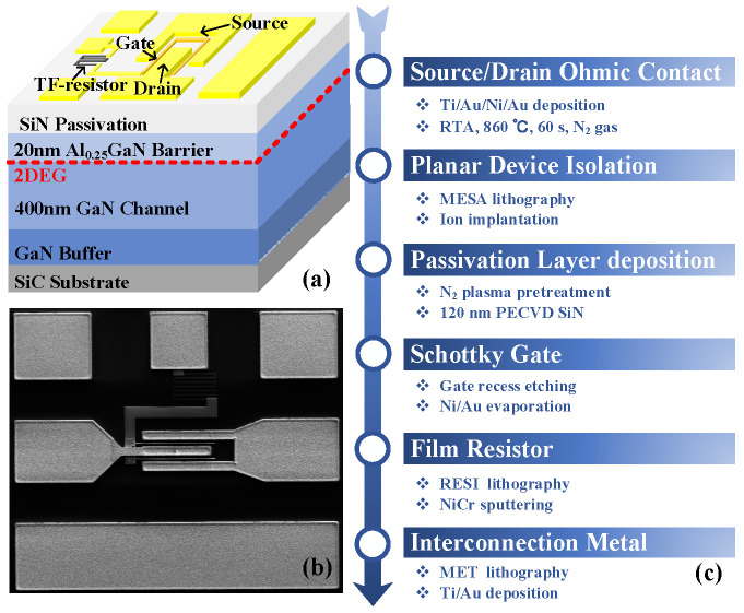 Figure 1
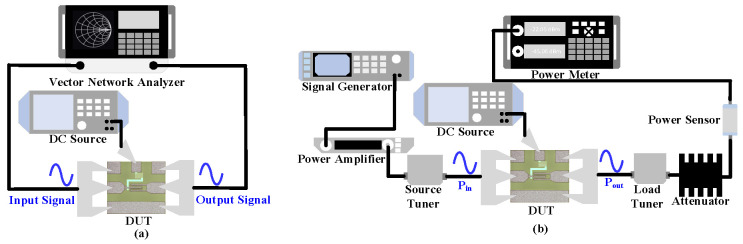 Figure 2
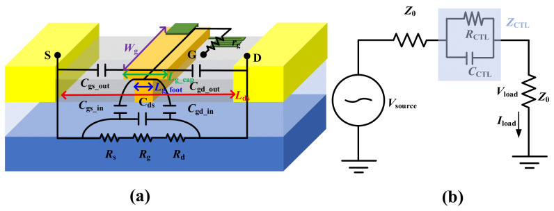 Figure 3
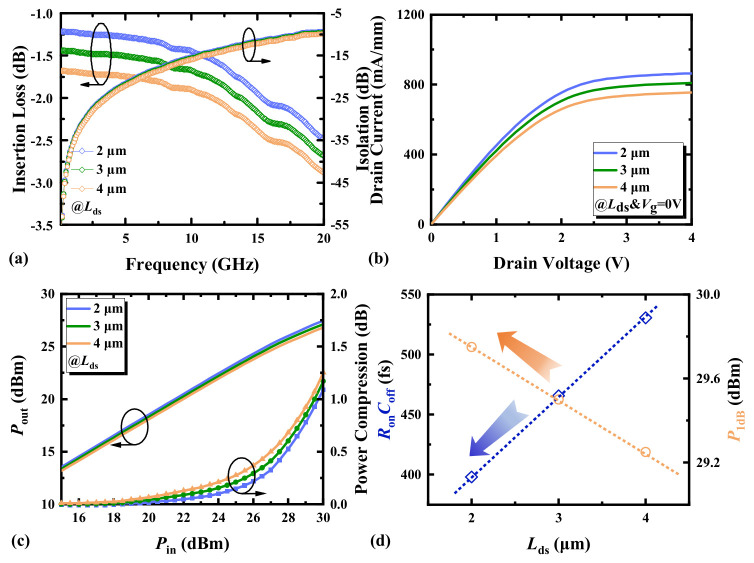 Figure 4
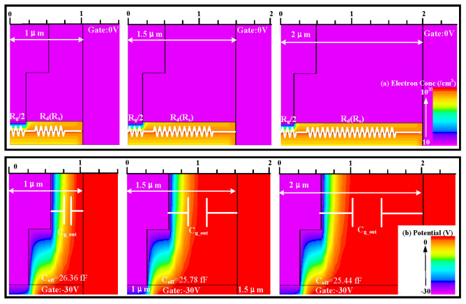 Figure 5
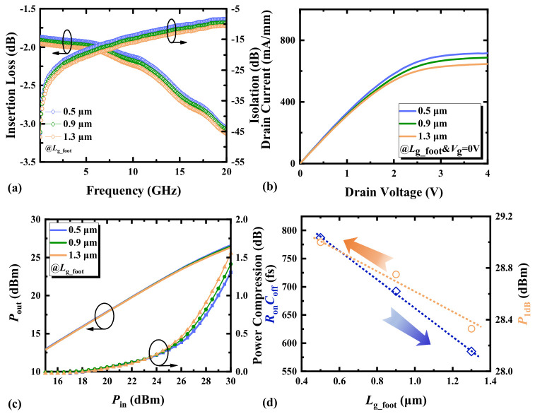 Figure 6
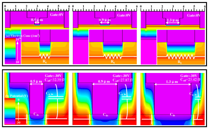 Figure 7
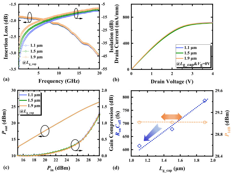 Figure 8
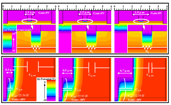 Figure 9
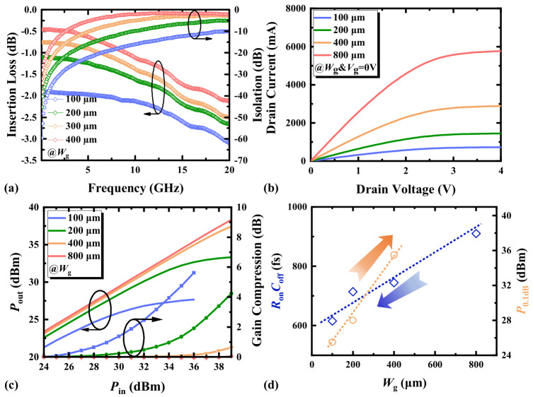 Figure 10
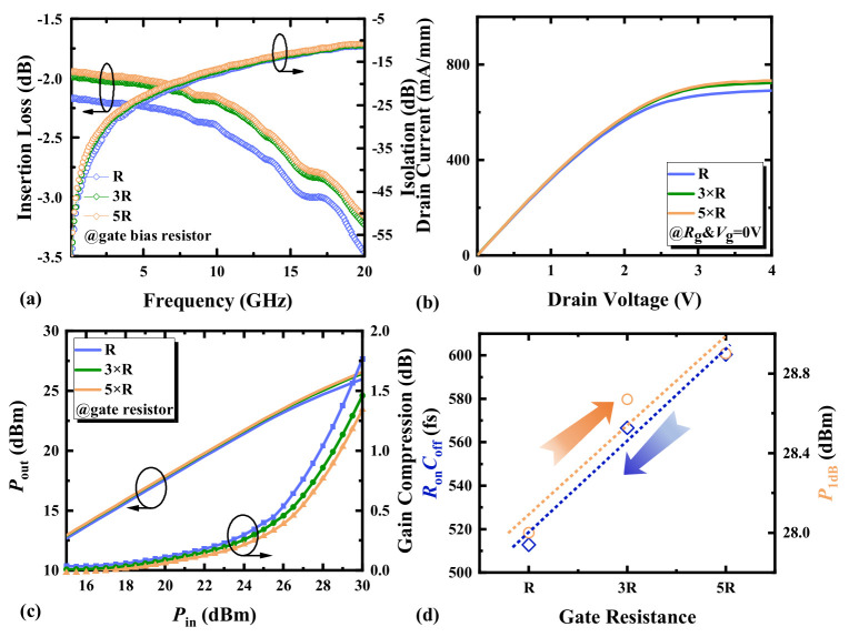 Figure 11
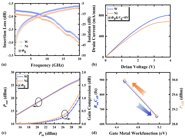 Figure 12
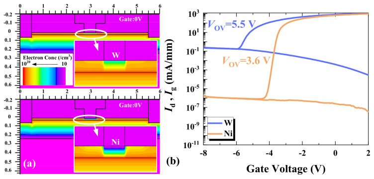 Figure 13
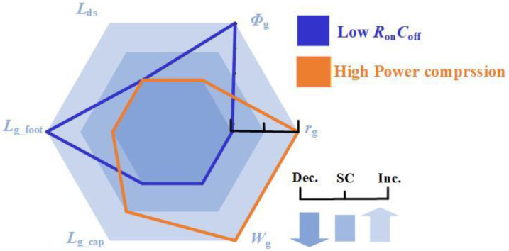 Figure 14
- —National Natural Science Foundation of China
- —China National Postdoctoral Program for Innovative Talents
- —China Postdoctoral Science Foundation
- —Fundamental Research Funds for the Central Universities of China
Peer Reviews
No public reviews on file for this paper yet. If you reviewed it on a platform where reviews are public (OpenReview, ICLR, NeurIPS, ICML), you can paste yours below so the community can read it here.
Videos
No videos yet. Explain this paper in a talk, walkthrough, or lecture? Add one.
Taxonomy
TopicsGaN-based semiconductor devices and materials · Advanced Power Amplifier Design · Silicon Carbide Semiconductor Technologies
1. Introduction
As an important part of RF front-end modules, RF switches are used in scenarios such as radar, base stations, and satellites and have always been popular for research. High-performance RF switches need low insertion loss (IL), high isolation (ISO), high power handling capability, and wide bandwidth.
Compared to microelectromechanical systems (MEMS) [1], PIN diode switches [2], and GaAs HEMTs [3], GaN HEMTs are gradually becoming the mainstream of high-power RF module applications due to their low power consumption, high RF performance, and easy integration in MMICs [4]. In the field of GaN-based RF switches, recent studies focused mainly on the direction of GaN-based RF switch MMIC circuits, usually based on the limited GaN process line scheme, by changing different circuit topologies to enhance the performance of GaN RF switches [5,6]; however, there are still relatively few studies on the influence of the device structure on the RF transmission performance and power handling of GaN HEMTs [7,8]. While numerous studies have focused on optimizing individual performance metrics, they have not systematically revealed the complex trade-off relationships that exist among different structural parameters, as well as between these parameters and multiple performance indicators. RF switches’ operating frequency and power compression capability are still the core challenges in this field.
This paper investigates the influence of device geometries, rg, and Φg on RonCoff and power compression of AlGaN/GaN HEMTs used as RF switch devices.
2. Device Structure and Fabrication
The conventional AlGaN/GaN HEMT for RF switch application was fabricated on the epitaxial structure, which was grown on substrate by metal–organic chemical vapor deposition (MOCVD) and consisted of an AlN nuclear layer, a GaN buffer layer, a GaN channel layer, and an AlGaN barrier layer from bottom to top. The 2DEG sheet density of the epitaxial material at room temperature was 1.071 × 10^13^ cm^−2^, with a sheet resistance of 333 Ω/sq. The device process was started by source and drain ohmic formation, including Ti/Al/Ni/Au metal stack evaporation and rapid annealing at N2 atmosphere at 860 °C for 60 s. After multilayer N+ injection to isolate the device, a 120 nm SiN passivation layer was deposited. A gate window was identified by photolithography and CF4-based plasma etching, and a T-shaped gate profile was realized using a Ni/Au or W/Au metal stack. A 30 nm NiCr thin film resistor was formed by sputtering. Finally, Ti/Au metal stack interconnections of the device were realized. The fabricated GaN HEMT RF switch device is shown in detail in Figure 1a–c.
Test structure layouts were specifically set for the characterization of RF switch. The device structure of the switch was symmetric (Lgs = Lgd) with a Schottky contact gate between the source and drain [9]. The ground-signal-ground (GSG) pads on both sides of the device serve as standard RF probe test interfaces, ensuring impedance matching and signal integrity during on-wafer high-frequency measurements. The independent gate bias pad is physically separated from the RF GSG structure, providing a DC feed path for the static gate voltage and preventing mutual interference between the RF signal and the DC bias circuit. A large resistor was added between the gate’s DC pad and the HEMT’s gate. The gate length is 500 nm, which is constrained by the lithography tool’s resolution limit to ensure process robustness. This choice does not hinder the clear and effective investigation of the core physical mechanisms mentioned above.
3. Measurement Results and Analysis
This paper pays attention to the mechanisms of how the dimensions and key processes of RF switch devices impact their small-signal and power characteristics, focusing on different Lds, Lg_foot, Lg_cap, Wg, rg, and Φg. Specific parameter settings and variables are detailed in Table 1.
This paper characterizes IL in the on-state and ISO in the off-state of the RF switch device through small signal testing. The test equipment setup is shown in Figure 2a, with the vector network analyzer (Agilent E8363B, Agilent Technologies, Santa Rosa, CA, USA) providing a small signal, which enters the source/drain terminals of the RF switch device. After selection, it is output from the drain/source terminals and finally enters the vector network analyzer to obtain S-parameters for analysis. Additionally, the RF switch device’s gate is externally connected to a DC source meter (Keysight B2902B, Keysight Technologies, Penang, Malaysia) to obtain the DC control bias.
Power compression refers to the phenomenon where the output power of an amplifier decreases as the input power exceeds a certain point. This phenomenon arises from nonlinearity in the device’s transfer characteristics, leading to a reduction in gain and output power above specific input levels.
This paper characterizes the power compression capability of the RF switch device in the on-state through load-pull testing. The construction of the test platform is shown in Figure 2b. The signal is generated by the signal source (Agilent E8257D), amplified by the driver amplifier (OPHIR5192, OPHIR Optronics Ltd., Jerusalem, Israel) to obtain a large signal. The signal passes through the RF switch device, and the output power is finally collected by the power probe and displayed by the power meter (Agilent N1912A). Additionally, the source/load tuner in the test system provides a fixed 50 Ω input and output impedance for the device under test, and the DC source meter Keysight B2902B provides gate bias [10]. During testing, large signals enter from the source/drain of the RF switch device and exit from the drain/source.
The simulation framework defines a physics-based model for simulating AlGaN/GaN HEMTs. The Shockley–Read–Hall (SRH) recombination model is enabled to capture the dominant carrier recombination mechanism via trap levels within the bandgap. A critical part of the model for GaN-based HEMTs involves the calculation of polarization charges. The simulator computes the strain within the heterostructure and, based on this strain and the material’s piezoelectric coefficients, derives the piezoelectric polarization charge. This is coupled with the inherent spontaneous polarization charge.
3.1. Source-Drain Spacing
Figure 3 shows the equivalent circuit of the switch device, which is composed of a series of intrinsic parameters. The small-signal performance of the switch device is analyzed starting from these parameters. IL or ISO is shown below [11]:
In Equation (1), Z0 is the load impedance, and RCTL is the resistance of the control element, which was mainly determined by the source-drain resistance (Rds) at the linear region. CCTL is the capacitance of the control element. PA is the load power without the control element, and Pload is the load power with the control element present. Moreover, rg is introduced to enhance ISO and reduce signal leakage [12]. RCTL can be expressed as follows [13,14]:
Rg, Rs, and Rd are the channel resistance, the source-gate, and drain-gate channel resistances, respectively. In the on-state, IL is predominantly influenced by RCTL, which is the on-state resistance (Ron) of the element.
In Equation (3), CCTL can be expressed by the following equation [15]:
where Cds, Cgd_out/Cgs_out, and Cgd_in/Cgs_in are the channel capacitance, the parasitic capacitance of gate to drain/source, and internal diode capacitance of gate to drain/source, respectively. For operation well below the switch cutoff frequency, the reactance of the off-state capacitance (Coff) is much greater than Roff, and so ZCTL ≈ CCTL ≈ Coff.
Figure 4a demonstrates a situation where the IL and ISO of the switching device both exhibit an increasing trend with the increase in Lds. From the simulation analysis in Figure 5, it can be seen that an increase in Lds leads to an increase in Rd and Rs, resulting in the degradation of IL. In addition, increasing Lds results in the decrease in capacitances Cgd_out and Cgs_out, while Cds remains unchanged; thus, Coff is reduced. This results in a slight improvement in ISO. Figure 4b indicates that increasing the source-drain spacing and, consequently, increasing the channel length forces the current to travel through a longer path, which may reduce the current density in the channel and affect power output. The switching power characteristics of HEMTs with different source-drain spacings are shown in Figure 4c. Figure 4d shows the influence of the variation in Lds of HEMTs on RonCoff and P1dB. The variation in Lds has a greater impact on Ron than on Coff, causing RonCoff to increase as Lds increases. Therefore, to improve the RF switching performance of HEMTs, the reduction in Lds can thereby reduce RonCoff. Reducing Lds can enhance the power handling capability of HEMTs, resulting in the improvement of the power compression of the large signal.
3.2. Gate Foot Length
The gate foot lengths of the HEMTs in this paper are all shorter than the gate cap lengths. Figure 6a indicates that as Lg_foot increases, both IL and ISO of the RF switch device increase. As shown in Figure 7, the change in gate foot length causes variations in the depletion region length due to the Schottky contact beneath the gate, where Rg is positively correlated with Lg_foot, and the influence of Rg is much greater than that of Rd and Rs, thereby leading to a change in Ron along with the trend of Rg variations. When HEMTs are in the off-state, an increase in Lg_foot leads to an increase in the equivalent channel capacitance spacing and a decrease in the parasitic capacitance area of the gate cap. As a result, the Cds and the Cgs_in/Cgd_in decrease and ISO improves.
As indicated in Figure 6b, an increase in Lg_foot results in a reduction in the current density of the switch and a shift in the knee voltage toward the negative direction. As Lg_foot increases, the knee voltage shifts towards more negative values due to alterations in the internal electric field distribution and carrier transport properties, resulting in reduced current density and affecting the point where current saturation begins, thus modifying the knee voltage [16]. Consequently, in Figure 6c, with an increase in Lg_foot of the HEMTs, the switch enters the compression phase at an earlier stage. Figure 6d shows the influence of the variation in Lg_foot of HEMTs on RonCoff. The influence of Lg_foot on Coff is greater than that on Ron. To obtain a better RonCoff product and stronger gate control capability, Lg_foot can be appropriately increased. It also reveals that the trends for selecting Lg_foot to achieve a low RonCoff and a high P1dB are opposite. Selecting an appropriate Lg_foot is beneficial for balancing the small signal performance and power handling of the switch device. This opposing trend clearly demonstrates that RonCoff, as a small-signal figure of merit, exhibits an inherent conflict between its optimization direction and the requirements for optimizing large-signal power performance. In the design of RF GaN HEMTs, a deliberate trade-off between these aspects must be made based on the target application. Consequently, RonCoff alone cannot be used to characterize or predict a device’s large-signal power handling capability.
3.3. Gate Cap Length
From Figure 8a, it can be observed that changing Lg_cap has little effect on the HEMTs’ IL. Figure 9 indicates that Lg_cap has a minimal impact on the depletion region formed by Schottky contact, resulting in an insignificant change in the electron concentration under the gate and an insignificant change in Rg. However, altering Lg_cap causes a significant change in ISO due to a substantial change in Coff in the off-state. Through the analysis of the potential in the off-state of the device, an increase in Lg_cap affects the capacitance Cgs_in/Cgd_in formed between the gate cap and the channel charge [17]. As indicated in Figure 9, this capacitance can be approximated as a parallel plate capacitor, where an increase in Lg_cap increases the parallel plate area, leading to an increase in Cgs_in/Cgd_in according to the capacitance formula. On the other hand, an increase in Lg_cap also reduces the distance between the gate cap and the source/drain ohmic contacts, which are the two plates, thus increasing the parasitic capacitance Cgd_out/Cgs_in. This results in an overall increase in Coff, leading to a degradation in device ISO as Lg_cap increases. Figure 8b,c indicates that the impact of different Lg_cap on the saturation current and power compression capability of HEMTs is not significantly pronounced. Figure 8d shows the influence of the variation in Lg_cap of HEMTs on RonCoff. Appropriately decreasing Lg_cap can assist HEMTs in attaining a smaller RonCoff.
3.4. Gate Width
Figure 10a demonstrates the study of IL and ISO with different gate widths. The research on the impact of Wg is relatively straightforward. As Wg increases, the cross-sectional area of the 2DEG channel also increases, allowing more electrons to participate in conduction, thereby reducing the channel resistances Rg, Rd, and Rs. The reduction in channel resistance can decrease the resistive loss of the device, thereby reducing IL. The relationship between resistive loss, channel resistance, and current is given by the following [18]:
In the off-state, a wider gate increases the overlap area between the gate and drain/source, leading to an increased Cgd/Cgs. This capacitance may induce additional parasitic currents, thereby degrading ISO between the input and output ports. Moreover, increasing Wg expands the depletion region, which enhances the internal inherent capacitances and consequently increases Cds. Overall, the Coff increases significantly, leading to degraded ISO.
As depicted in Figure 10b, the expansion of the effective conductive area with increasing Wg reduces the on-resistance, thereby improving the device’s overcurrent capability. A reduced on-resistance minimizes conduction losses in the on-state, while enhanced overcurrent capability enables higher power-handling capacity in the device [19]. As shown in Figure 10c, HEMTs with larger W_g_ exhibit higher power compression capabilities, making them more widely applicable in high-power RF modules. Figure 10d indicates that the trends for selecting Wg to achieve a low RonCoff and a high P0.1dB are opposite. The influence of Wg on Coff is greater than that on Ron. Therefore, RonCoff increases as Wg increases. From the perspective of Wg design, there exists an inherent trade-off between improving power tolerance and RonCoff performance.
3.5. Gate Bias Resistance
Figure 11a focuses on the small-signal characteristics of HEMTs with different rg. As rg increases, IL is optimized at the expense of ISO degradation. The RF switch device’s Y-parameters are as follows [20,21]:
By converting Y-parameters to S-parameters, S21 can be expressed as follows [11,22]:
The equivalent circuit of RF switch devices can be represented by Yctl. In Equations (5)–(9), analysis of the admittance matrix elements y11 and y22 demonstrates that increasing rg enhances the Cg-to-ground decoupling. This improved decoupling effect reduces port-ground reflections, consequently increasing the magnitude of S21. This indicates that an increase in rg will reduce IL to some extent. In the off-state, increasing rg enhances the C_g_-to-ground decoupling effect, thereby diminishing gate-channel control efficacy. The underlying mechanism involves the substantial gate resistance generating an additional voltage drop that causes the effective gate potential at the Schottky interface to become more positive relative to the external DC bias. This potential shift results in a measurable degradation of ISO.
As observed from Figure 11b, for RF switch devices with gate biased at 0 V, a smaller rg weakens the Cg-to-ground decoupling effect. Consequently, this enhances gate control capability, accelerating current saturation while reducing channel current density. Such current density degradation ultimately compromises power output performance. As shown in Figure 11c, when rg increases, the fluctuations in gate voltage increase, leading to intensified nonlinear behavior of the device and more severe power compression. It is known that increasing rg reduces IL, and a larger rg can reduce power leakage through the gate, thereby decreasing losses. As rg continues to increase, these differences diminish. Figure 11d shows the influence of the variation in rg of HEMTs on RonCoff and P1dB. Increasing rg will improve the power handling capability of HEMTs, but it will deteriorate RonCoff. When selecting bias resistance, it is necessary to balance RonCoff and power compression.
3.6. Gate Metal Work Function
Figure 12a shows the small-signal switching characteristics with different Φg. The two metals used for forming the Schottky contact gates are tungsten (W) and nickel (Ni). The work function of W is 4.55 eV, while that of Ni is 5.15 eV. IL of HEMTs with W as the gate metal is lower than that with Ni, but its ISO is worse. Φg directly affects the charge distribution and control capability between the gate and the channel [23,24]. As shown in Figure 12b,c, higher Φg can lead to the early saturation of electron velocity in the channel, resulting in a lower current density and faster power compression.
From the simulation and measurement results shown in Figure 13, it is evident that when the gate bias is 0 V, HEMTs operate in the on-state, and the electron concentration under the W gate is significantly higher than that under the Ni gate. Different Φg results in different threshold voltages (Vth). At Vg = 0 V, this leads to distinct overdrive voltages (Vov = Vg − Vth) and different saturation current densities. Theoretically, the lower work function of W yields a more negative Vth, higher Vov, larger drain current density, better IL, and higher P1 dB at Vg = 0 V. Conversely, at Vg = −30 V, the reduced negative Vov degrades ISO.
Figure 12d illustrates the impact of Φg variation on RonCoff and P1 dB in HEMT devices. Increasing Φg can reduce the product of RonCoff, but it will lower P1 dB. The appropriate Φg is beneficial for balancing low RonCoff and high power-handling capability. These statements clarify that the influence patterns of the work function revealed in this study were characterized under the specific applied DC bias conditions. The conclusions directly reflect the core mechanism by which the work function difference alters the threshold voltage through flat-band voltage modulation near this specific operating point.
Figure 14 presents the design principle for low RonCoff and high power compression. As shown in Figure 14, when selecting the values of Lg_foot, Wg, rg, and Φg for HEMTs, a trade-off needs to be made between low RonCoff and high power compression. Subsequent optimization of the gate structure and selection of appropriate gate metals enabled the tailoring of AlGaN/GaN HEMTs for diverse RF switch applications.
4. Conclusions
In this paper, we investigated the structure-dependent parameter trade-off optimization on RonCoff and power compression of AlGaN/GaN HEMTs for RF switch application. It was found that RonCoff can be effectively reduced by increasing Lg_foot, decreasing Lg_cap, reducing rg, and adopting a high Φg. But these parameter modifications exhibit antagonistic effects on power compression and RonCoff. These results provide design guidelines for RF switch devices operating in diverse application environments.
The reference list from the paper itself. Each links out to its DOI / PubMed record.
- 1Liu Y. Bey Y. Liu X. High-Power High-Isolation RF-MEMS Switches With Enhanced Hot-Switching Reliability Using a Shunt Protection Technique IEEE Trans. Microw. Theory Tech.2017653188319910.1109/TMTT.2017.2687427 · doi ↗
- 2Yang J.G. Yang K. High-Linearity K-Band Absorptive-Type MMIC Switch Using Ga N PIN-Diodes IEEE Microw. Wirel. Compon. Lett.201323373910.1109/LMWC.2012.2234732 · doi ↗
- 3Mei P.-I. Wu G.-W. Hsu H.-S. Huang T.-J. Tsao Y.-F. Chiang C.-Y. Hsu H.-T. Single-Pole Double-Throw Switch Using Stacked-FET Configuration at Millimeter Wave Frequencies Proceedings of the 2018 Asia-Pacific Microwave Conference (APMC)Kyoto, Japan 6–9 November 2018791793
- 4Campbell C.F. Dumka D.C. Wideband High Power Ga N on Si C SPDT Switch MMI Cs Proceedings of the 2010 IEEE MTT-S International Microwave Symposium Anaheim, CA, USA 23–28 May 2010145148
- 5Thome F. Bruckner P. Quay R. Ambacher O. Millimeter-Wave Single-Pole Double-Throw Switches Based on a 100-Nm Gate-Length Al Ga N/Ga N-HEMT Technology Proceedings of the 2019 IEEE MTT-S International Microwave Symposium (IMS)Boston, MA, USA 2–7 June 201914031406
- 6Thome F. Leuther A. Ambacher O. Low-Loss Millimeter-Wave SPDT Switch MMI Cs in a Metamorphic HEMT Technology IEEE Microw. Wirel. Compon. Lett.20203019720010.1109/LMWC.2019.2958209 · doi ↗
- 7Erturk V. Gurdal A. Ozbay E. A High-Power and Broadband Ga N SPDT MMIC Switch Using Gate-Optimized HEM Ts IEEE Microw. Wirel. Technol. Lett.2023331207121010.1109/LMWT.2023.3275105 · doi ↗
- 8Lucci L. Charlet I. Gobil Y. Morisot F. Delprato J. Ruel S. Benotmane C. Laulagnet F. Dezest P. Bon R. CMOS Compatible 200 Mm Ga N-on-Si HEM Ts for RF Switch Applications with 36 d Bm CW Power Handling and 200 FS Ron Coff Proceedings of the 2024 IEEE International Electron Devices Meeting (IEDM)San Francisco, CA, USA 7–11 December 202414