Direct observation of 3D nitrogen distribution in silicon-based dielectrics using atom probe tomography
Byeong-Gyu Chae, Jeong Yeon Won, Young Sik Shin, Dong Jin Yun, Jae min Ahn, Seon Tae Park, Ki-bum Lee, Hokyun An, Mina Seol, I-Jun Ro, Se-Ho Kim, Chunhyung Chung, Eunha Lee

TL;DR
This paper uses atom probe tomography to directly observe nitrogen distribution in silicon-based semiconductors, revealing how it affects device performance and reliability.
Contribution
The study introduces advanced atom probe tomography techniques for precise 3D nitrogen mapping in semiconductor devices without isotope doping.
Findings
Nitrogen distribution in gate dielectrics influences impurity diffusion and electrical properties.
3D nitrogen profiles were mapped in 2- and 5-nm-thick gate dielectrics and fin-structured devices.
The results provide atomic-scale insights for improving semiconductor device reliability.
Abstract
The distribution of nitrogen in semiconductor devices plays a crucial role in tuning their physical and electrical properties. However, direct observation and precise quantification of nitrogen remain challenging because of analytical limitations, particularly at critical interfaces in silicon-based semiconductors. Although atom probe tomography has emerged as a powerful tool, distinguishing nitrogen from silicon without isotope doping is persistently difficult. In this study, we employ advanced atom probe tomography with an extended flight path under optimized conditions to characterize the three-dimensional nitrogen distribution in actual device structures, including 2- and 5-nm-thick silicon dioxide/silicon oxynitride-based gate dielectrics and a fin-structured three-dimensional device. Our analysis reveals that the nitrogen distribution determines the formation of the nitrogen…
Genes, proteins, chemicals, diseases, species, mutations and cell lines named across the full text — each resolved to its canonical identifier and authoritative record.
Click any figure to enlarge with its caption.
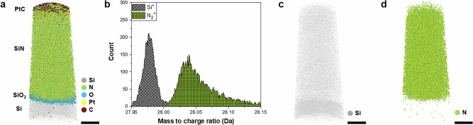 Figure 1
 Figure 2
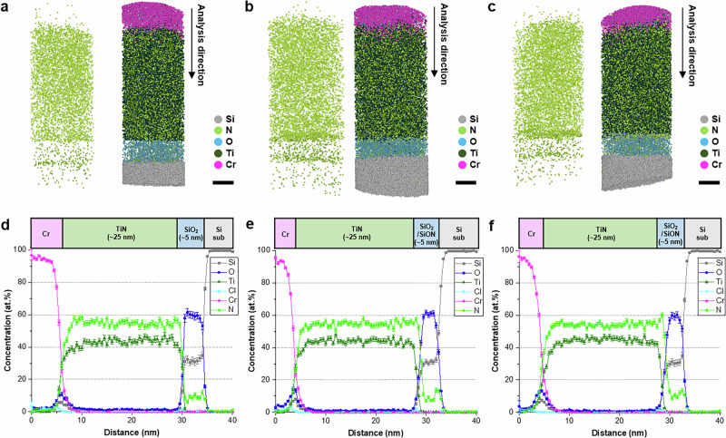 Figure 3
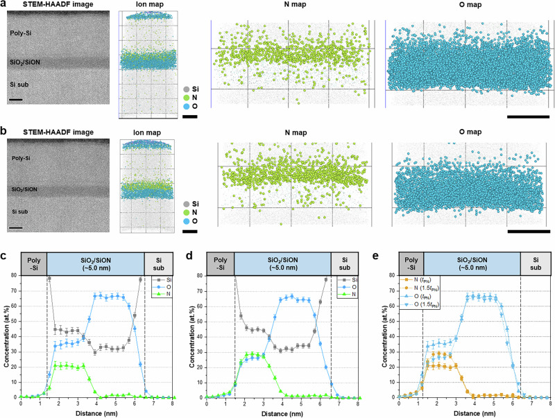 Figure 4
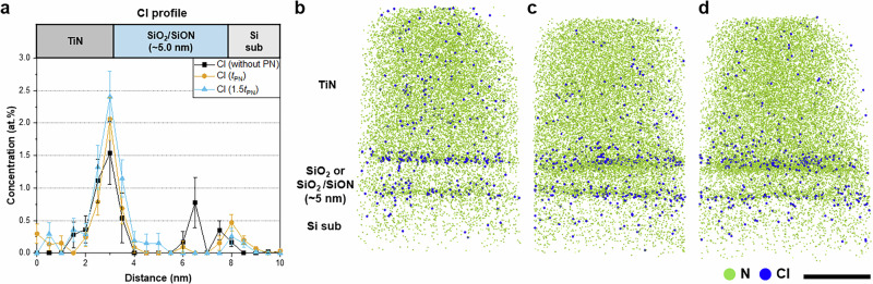 Figure 5
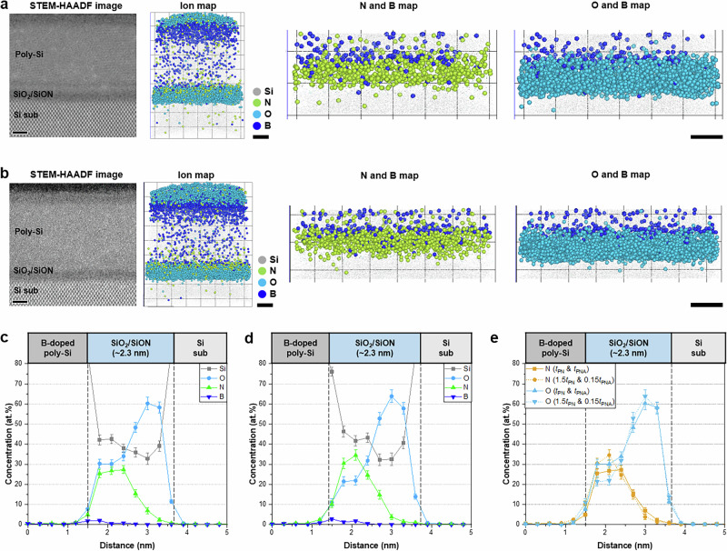 Figure 6
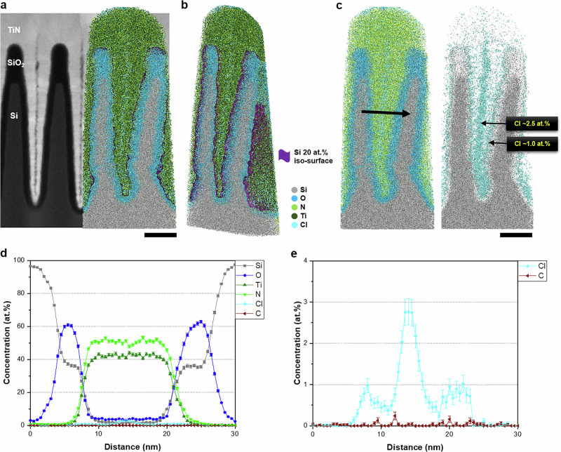 Figure 7
Peer Reviews
No public reviews on file for this paper yet. If you reviewed it on a platform where reviews are public (OpenReview, ICLR, NeurIPS, ICML), you can paste yours below so the community can read it here.
Videos
No videos yet. Explain this paper in a talk, walkthrough, or lecture? Add one.
Taxonomy
TopicsAdvanced Materials Characterization Techniques · Diamond and Carbon-based Materials Research · Electronic and Structural Properties of Oxides