Influence of Homoepitaxial Layer Thickness on Flatness and Chemical Mechanical Planarization Induced Scratches of 4H-Silicon Carbide Epi-Wafers
Chi-Hsiang Hsieh, Chiao-Yang Cheng, Yi-Kai Hsiao, Zi-Hao Wang, Chang-Ching Tu, Chao-Chang Arthur Chen, Po-Tsung Lee, Hao-Chung Kuo

TL;DR
This paper explores how the thickness of homoepitaxial layers affects the flatness and scratch resistance of 4H-SiC wafers used in high-voltage power devices.
Contribution
The study reveals how epitaxial thickness influences wafer deformation and scratch propagation under manufacturing conditions.
Findings
Increasing epitaxial thickness beyond 31 μm leads to significant geometric deformation.
Hydrogen etching and buffer layers reduce scratch propagation from CMP.
CMP-induced scratches are mitigated during epitaxial growth under HVM conditions.
Abstract
The integration of thick homoepitaxial layers on silicon carbide (SiC) substrates is critical for enabling high-voltage power devices, yet it remains challenged by substrate surface quality and wafer geometry evolution. This study investigates the relationship between substrate preparation—particularly chemical mechanical planarization (CMP)—and the impact on wafer bow, total thickness variation (TTV), local thickness variation (LTV), and defect propagation during epitaxial growth. Seven 150 mm, 4° off-axis, prime-grade 4H-SiC substrates from a single ingot were processed under high-volume manufacturing (HVM) conditions and grown with epitaxial layers ranging from 12 μm to 100 μm. Metrology revealed a strong correlation between increasing epitaxial thickness and geometric deformation, especially beyond 31 μm. Despite initial surface scratches from CMP, hydrogen etching and buffer layer…
Genes, proteins, chemicals, diseases, species, mutations and cell lines named across the full text — each resolved to its canonical identifier and authoritative record.
Click any figure to enlarge with its caption.
 Figure 1
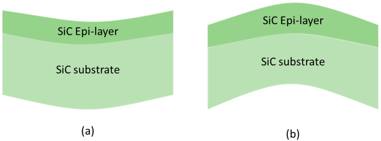 Figure 2
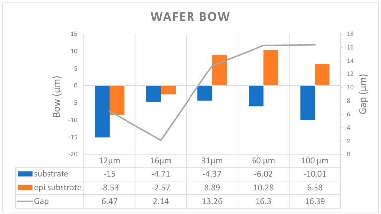 Figure 3
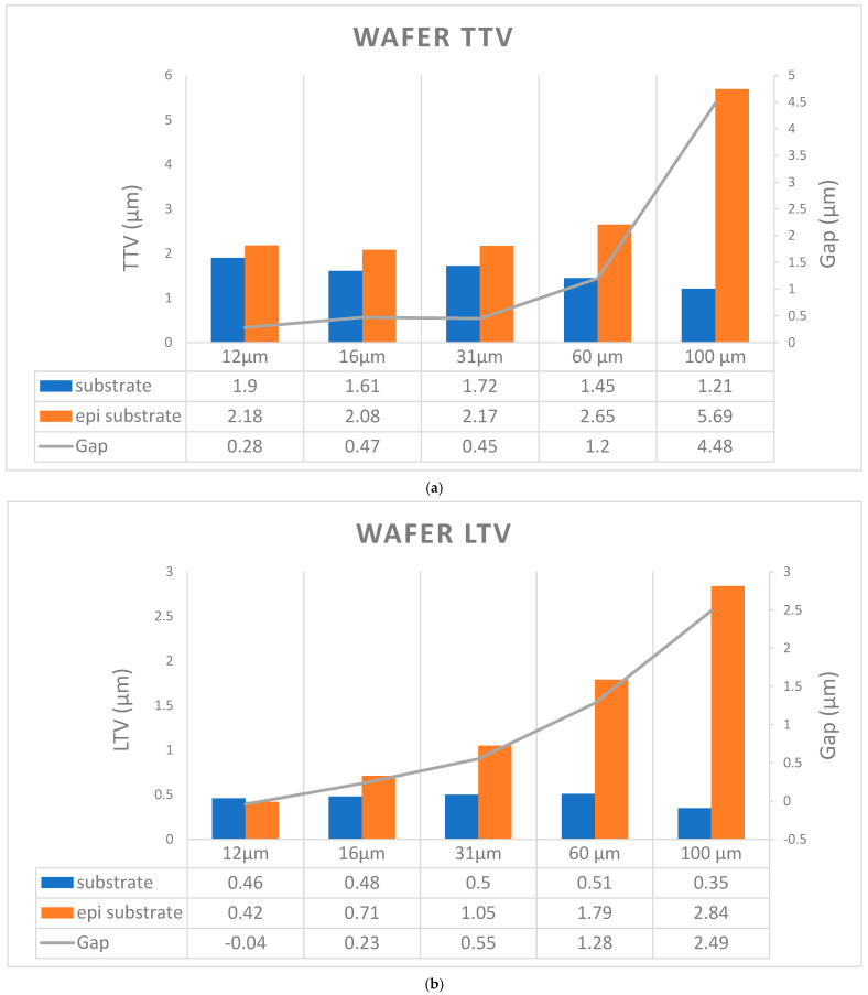 Figure 4
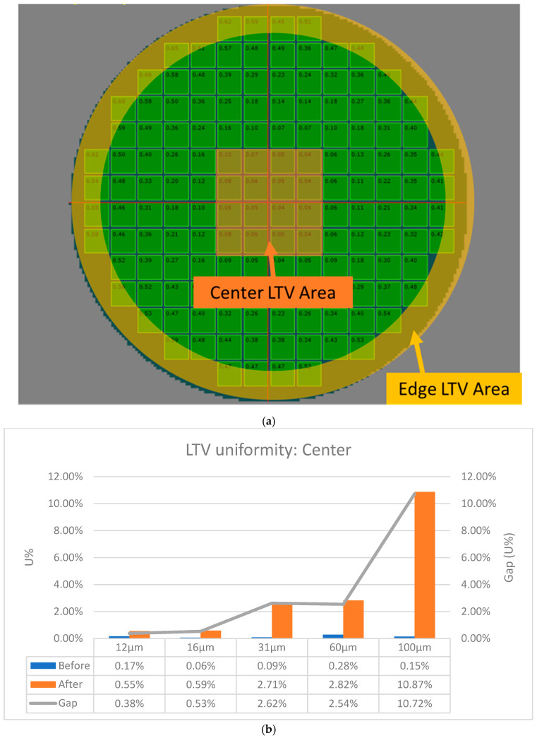 Figure 5
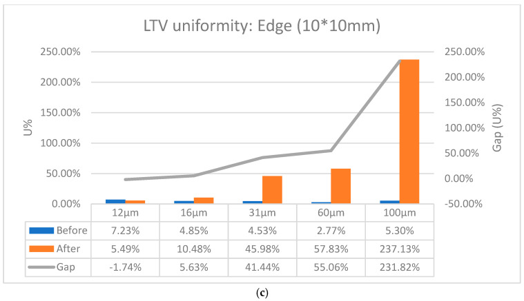 Figure 6
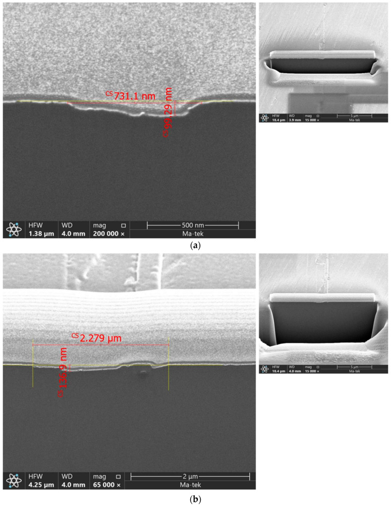 Figure 7
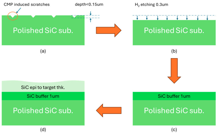 Figure 8
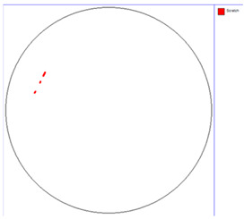 Figure 9
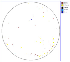 Figure 10
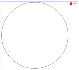 Figure 11
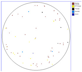 Figure 12
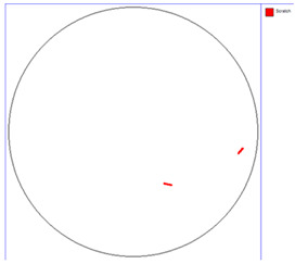 Figure 13
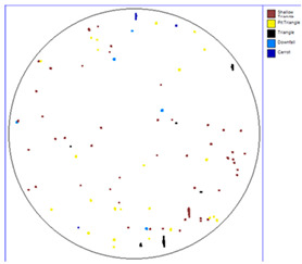 Figure 14
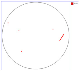 Figure 15
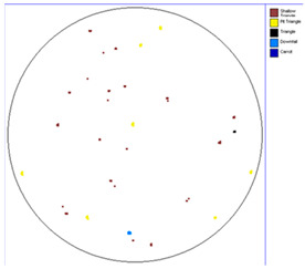 Figure 16
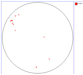 Figure 17
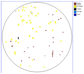 Figure 18
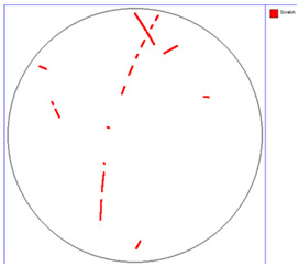 Figure 19
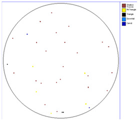 Figure 20
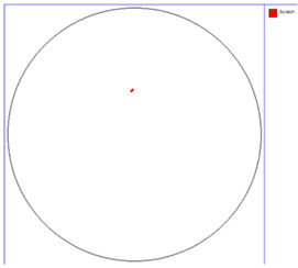 Figure 21
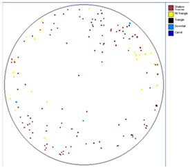 Figure 22
Peer Reviews
No public reviews on file for this paper yet. If you reviewed it on a platform where reviews are public (OpenReview, ICLR, NeurIPS, ICML), you can paste yours below so the community can read it here.
Videos
No videos yet. Explain this paper in a talk, walkthrough, or lecture? Add one.
Taxonomy
TopicsAdvanced Surface Polishing Techniques · Silicon Carbide Semiconductor Technologies · Copper Interconnects and Reliability