A CMOS-Compatible Process for ≥3 kV GaN Power HEMTs on 6-inch Sapphire Using In Situ SiN as the Gate Dielectric
Jie Zhang, Xiangdong Li, Jian Ji, Shuzhen You, Long Chen, Lezhi Wang, Zilan Li, Yue Hao, Jincheng Zhang

TL;DR
This paper presents a new process for making high-voltage GaN transistors on sapphire substrates, suitable for power electronics.
Contribution
A CMOS-compatible process for fabricating GaN HEMTs on 6-inch sapphire with ≥3 kV breakdown voltage is developed.
Findings
GaN HEMTs with 18.06 Ω·mm RON and 3 kV breakdown voltage were fabricated on 6-inch sapphire.
Uniform VTH and RON were achieved across the wafer using a 1.5 µm GaN buffer and 20 nm in situ SiN gate dielectric.
Electrical mapping confirmed high uniformity of device performance across the wafer.
Abstract
The application of GaN HEMTs on silicon substrates in high-voltage environments is significantly limited due to their complex buffer layer structure and the difficulty in controlling wafer warpage. In this work, we successfully fabricated GaN power HEMTs on 6-inch sapphire substrates using a CMOS-compatible process. A 1.5 µm thin GaN buffer layer with excellent uniformity and a 20 nm in situ SiN gate dielectric ensured uniformly distributed VTH and RON across the entire 6-inch wafer. The fabricated devices with an LGD of 30 µm and WG of 36 mm exhibited an RON of 18.06 Ω·mm and an off-state breakdown voltage of over 3 kV. The electrical mapping visualizes the high uniformity of RON and VTH distributed across the whole 6-inch wafer, which is of great significance in promoting the applications of GaN power HEMTs for medium-voltage power electronics in the future.
Click any figure to enlarge with its caption.
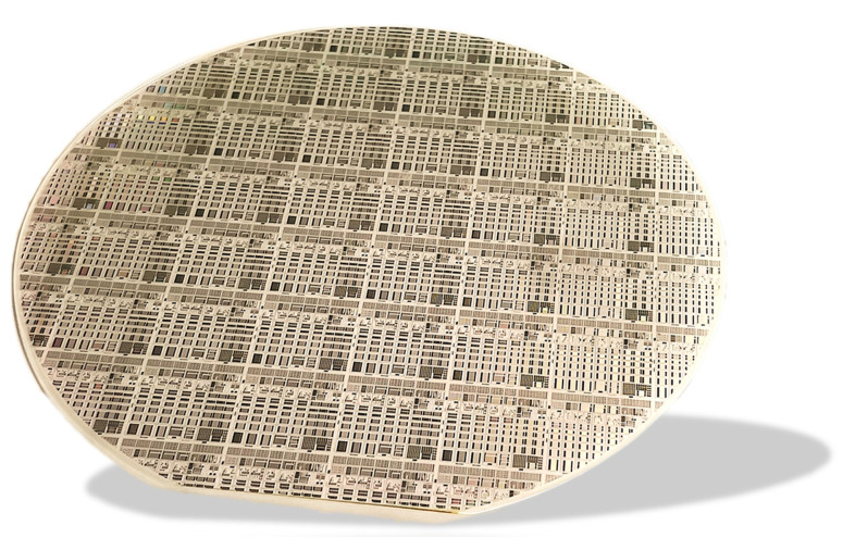 Figure 1
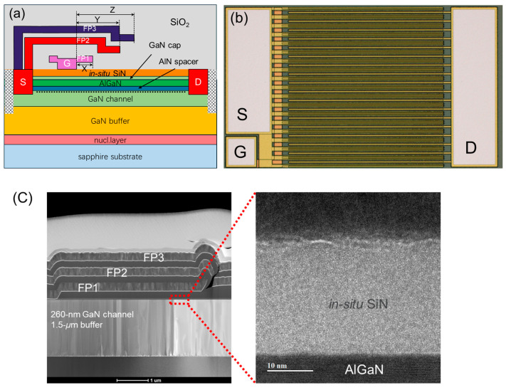 Figure 2
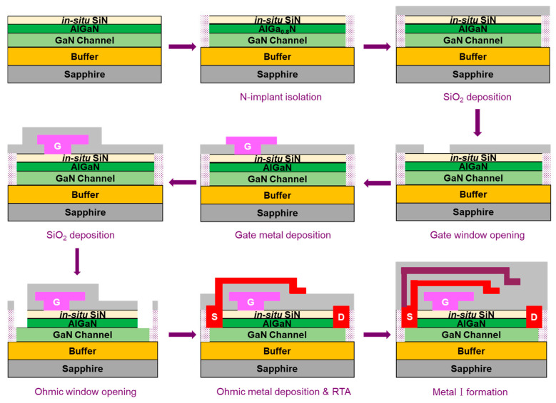 Figure 3
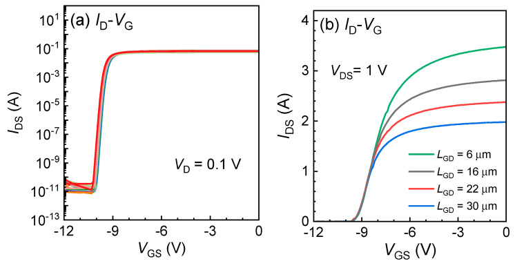 Figure 4
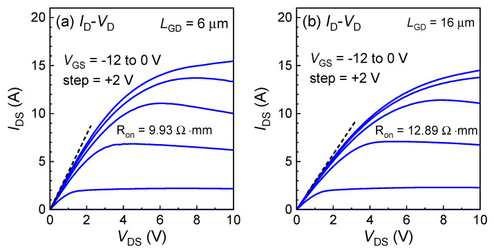 Figure 5
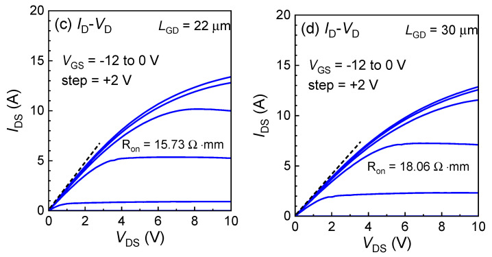 Figure 6
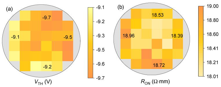 Figure 7
 Figure 8
 Figure 9
 Figure 10
 Figure 11
Peer Reviews
No public reviews on file for this paper yet. If you reviewed it on a platform where reviews are public (OpenReview, ICLR, NeurIPS, ICML), you can paste yours below so the community can read it here.
Videos
No videos yet. Explain this paper in a talk, walkthrough, or lecture? Add one.
Taxonomy
TopicsGaN-based semiconductor devices and materials · Silicon Carbide Semiconductor Technologies · Semiconductor materials and devices