Current-induced atomic forces in gated graphene nanoconstrictions
Susanne Leitherer, Nick Papior, Mads Brandbyge

TL;DR
This study uses ab-initio density functional theory to analyze how electronic currents induce atomic forces in gated graphene nanoconstrictions, revealing complex relationships between forces, charges, and voltage profiles.
Contribution
It provides a detailed ab-initio analysis of current-induced atomic forces in graphene nanostructures, linking forces to charge distribution and voltage drop effects.
Findings
Current-induced bond-forces are correlated with bond-charges.
Bond-forces are not simply correlated with bond-currents.
Voltage drop across the junction influences the magnitude of atomic forces.
Abstract
Electronic current densities can reach extreme values in highly conducting nanostructures where constrictions limit current. For bias voltages on the 1 volt scale, the highly non-equilibrium situation can influence the electronic density between atoms, leading to significant inter-atomic forces. An easy interpretation of the non-equilibrium forces is currently not available. In this work, we present an ab-initio study based on density functional theory of bias-induced atomic forces in gated graphene nanoconstrictions consisting of junctions between graphene electrodes and graphene nano-ribbons in the presence of current. We find that current-induced bond-forces and bond-charges are correlated, while bond-forces are not simply correlated to bond-currents. We discuss, in particular, how the forces are related to induced charges and the electrostatic potential profile (voltage drop) across…
Click any figure to enlarge with its caption.
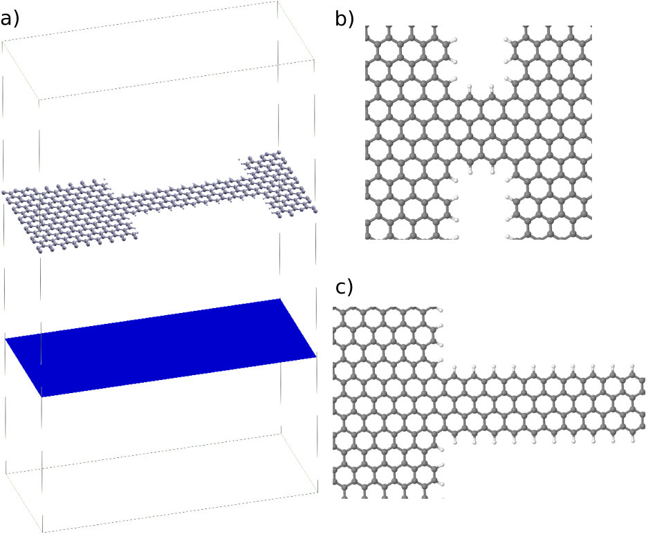 Figure 1
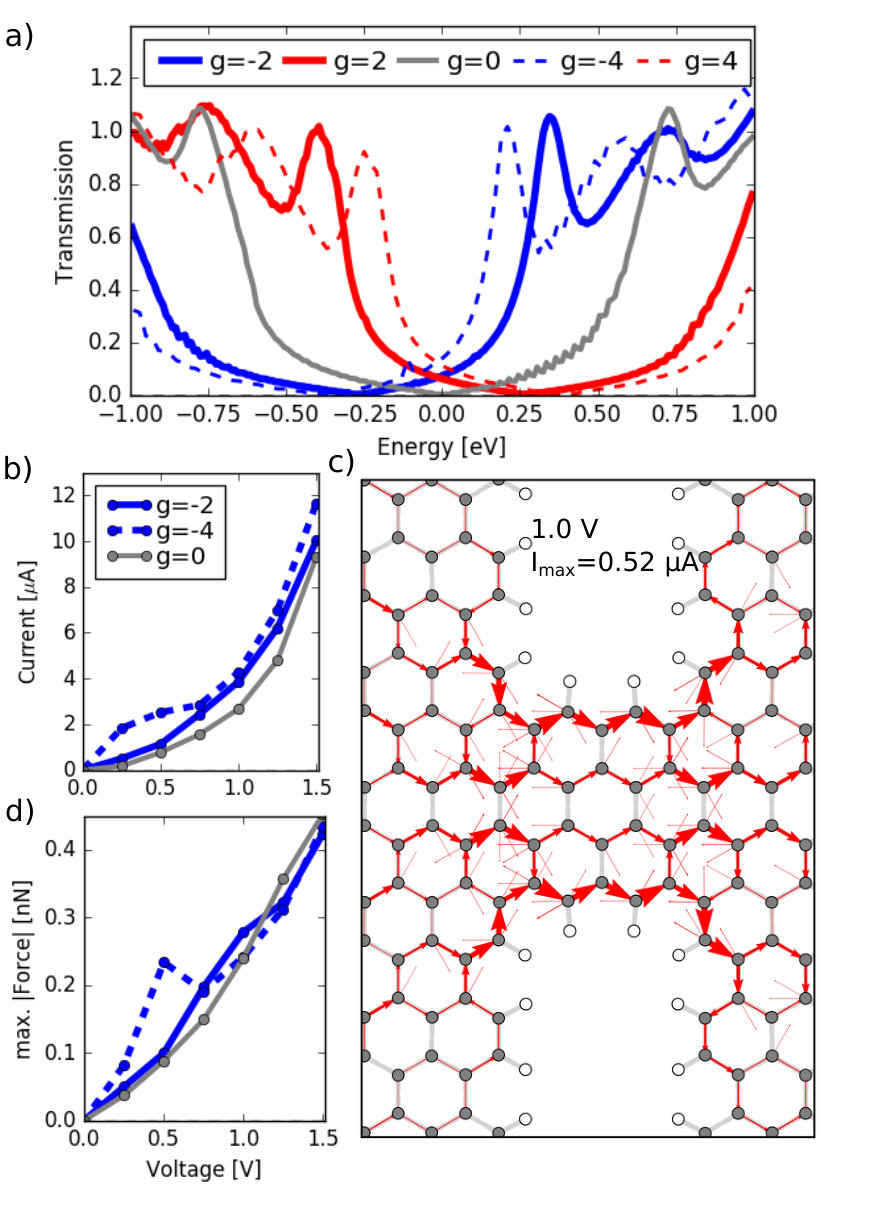 Figure 2
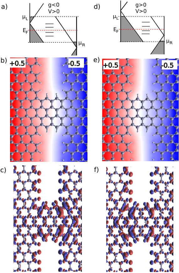 Figure 3
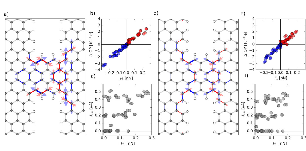 Figure 4
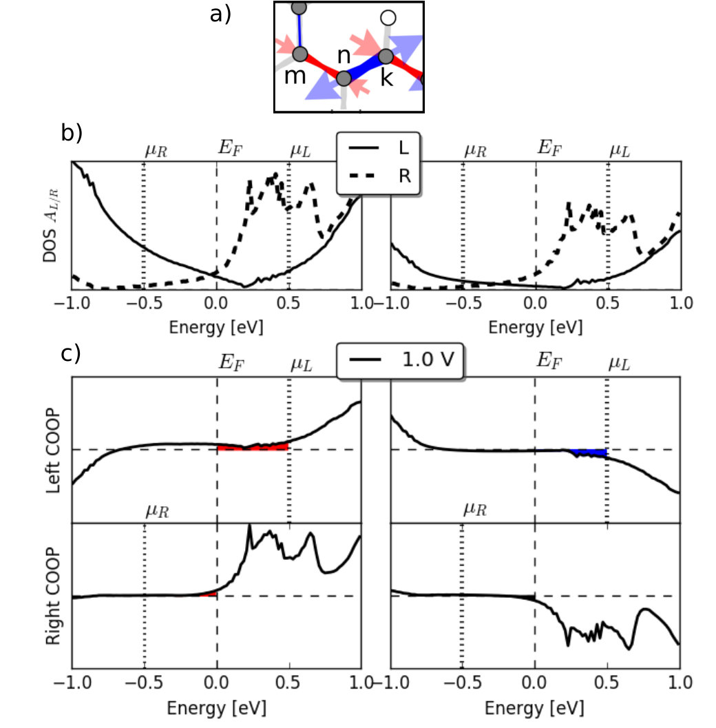 Figure 5
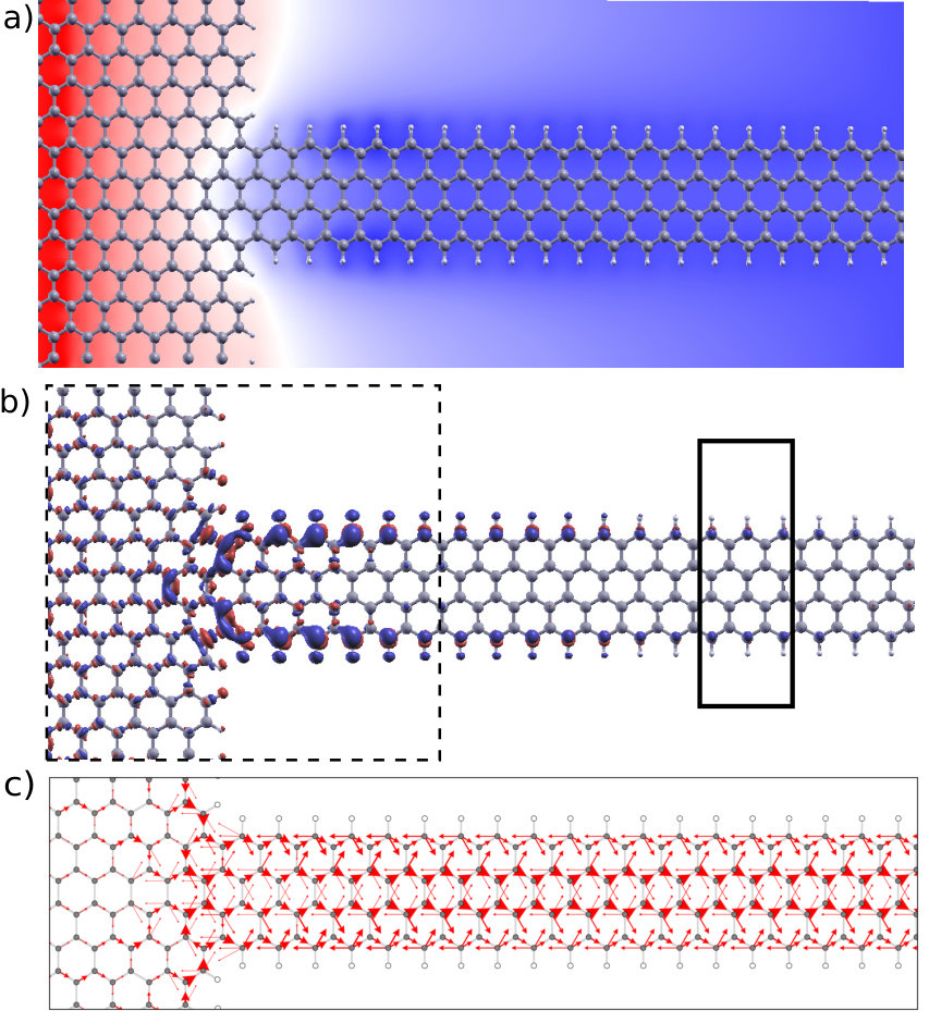 Figure 6
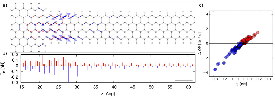 Figure 7
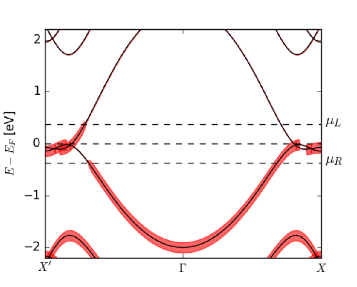 Figure 8
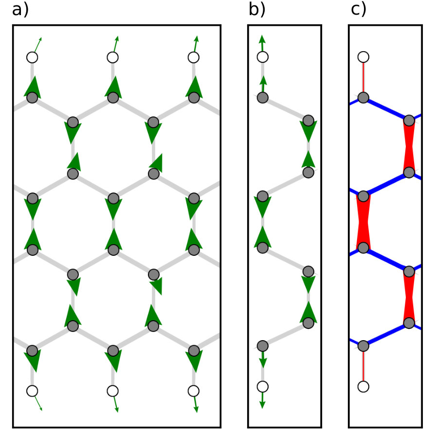 Figure 9
Peer Reviews
No public reviews on file for this paper yet. If you reviewed it on a platform where reviews are public (OpenReview, ICLR, NeurIPS, ICML), you can paste yours below so the community can read it here.
Videos
No videos yet. Explain this paper in a talk, walkthrough, or lecture? Add one.
Current-induced atomic forces in gated graphene nanoconstrictions
S. Leitherer
Center for Nanostructured Graphene, Department of Physics, Technical University of Denmark, DK-2800 Kongens Lyngby, Denmark
N. Papior
Department of Applied Mathematics and Computer Science, Technical University of Denmark, DK-2800 Kongens Lyngby, Denmark
M. Brandbyge
Center for Nanostructured Graphene, Department of Physics, Technical University of Denmark, DK-2800 Kongens Lyngby, Denmark
Abstract
Electronic current densities can reach extreme values in highly conducting nanostructures where constrictions limit current. For bias voltages on the 1 volt scale, the highly non-equilibrium situation can influence the electronic density between atoms, leading to significant inter-atomic forces. An easy interpretation of the non-equilibrium forces is currently not available. In this work, we present an ab-initio study based on density functional theory of bias-induced atomic forces in gated graphene nanoconstrictions consisting of junctions between graphene electrodes and graphene nano-ribbons in the presence of current. We find that current-induced bond-forces and bond-charges are correlated, while bond-forces are not simply correlated to bond-currents. We discuss, in particular, how the forces are related to induced charges and the electrostatic potential profile (voltage drop) across the junctions. For long current-carrying junctions we may separate the junction into a part with a voltage drop, and a part without voltage drop. The latter situation can be compared to a nano-ribbon in the presence of current using an ideal ballistic velocity-dependent occupation function. This shows how the combination of voltage drop and current give rise to the strongest current-induced forces in nanostructures.
I Introduction
The current densities in nano-scale, ballistic conductors can reach extreme values compared to macroscopic Ohmic conductors. For example, the break-down voltages of atomic chains of Au are beyond corresponding to a current-densitySabater et al. (2015) on the order of , and the current-carrying capacity of narrow graphene conductors can reach almost before breakdown.Moser et al. (2007) From a technological point of view the nano regime poses challenges in terms of stability and reproducibility, since in this extreme scaling limit the position of a few atoms control the device operation.
On the other hand, atomic control of the structure by external driving forces offers an enormous potential for further downscaling. F.ex. it has been demonstrated in experiments how the current/field may be used to toggle switch atomic-scale contacts between different conductance states corresponding to different atomic configurations of metallic nano-contacts.Schirm et al. (2013)
In this paper we will concentrate on another important example, namely graphene nanostructures, which are now being created and changed using high applied voltages and consequently electrical current. Due to its excellent electrical and mechanical properties, graphene is a promising material for two-dimensional (2D) nanoelectronic applications.Geim and Novoselov (2007) So-called ”electro-burning“ has been employed in experiments to fabricate nano-gaps between graphene electrodes.Sadeghi et al. (2015) These electrodes of single or few-layer graphene has in some cases subsequently been bridged by single molecules.Prins et al. (2011); Ullmann et al. (2015); Leitherer et al. (2017); Sun et al. (2018) Using similar techniques, the fabrication of electrically switchable graphene break junctions has been reported.Zhang et al. (2012); Standley et al. (2008) Electron microscopy allows for structural, atomic-scale studies of graphene structures in the presence of high current and applied voltage.Harris (2017) It has been seen how the structure of edges are changed by the current/voltageJia et al. (2009) or how layers fuse.Barreiro et al. (2012) Current-induced motion/cleaning of adsorbed species on graphene has also been investigated.Moser et al. (2007)
Under high bias and current density a number of different, possibly intertwined, effects play crucial roles for the atomic configuration, such as motion driven by locally induced fields, Joule heating and temperature gradients, as well as current-induced forces due to a steady momentum transfer from electronic current to ions.Dundas et al. (2009); Di Ventra et al. (2002); Lü et al. (2015) Common for these structures and effects in graphene nanostructures is that the electrons may to a large degree be in the ballistic quantum transport regime, as seen e.g. by the appearance of interference phenomena.Sadeghi et al. (2015); García-Suárez et al. (2018); Gehring et al. (2016) Experiments performed at high voltage bias on a bilayer constriction show an uniaxial lattice expansion of more than 5% at a current density on the order of before breaking.Börrnert et al. (2012)
The understanding of the role of voltage and currents in such systems and processes are still rudimentary. We consider here a simple, narrow graphene ribbon system using first principles calculations based on Density Functional Theory combined with Non-Equilibrium Greens functions (DFT-NEGF). We have previously studied the electron-phonon interaction in transport and the voltage drop dependence on gating in this system.Gunst et al. (2016); Papior et al. (2016) In this paper we consider the current-induced forces in the presence of steady-state electronic current, and analyze these in terms of the changes in electronic distributions.
Our DFT-NEGF calculations, presented in the first part of this work, return forces for systems that are defected in the sense of having a scattering region. However, for ballistic bulk systems one could imagine a current flowing which is far from any scattering potential, and approximately behaves as though states are occupied depending on their velocity. We present this approach and compare to the DFT-NEGF forces in the last part of this paper (Sec. III.2.2).
II Setup and Method
The systems we investigate are constrictions consisting of graphene nanoribbons (GNRs) of varying lengths, placed between graphene electrodes (cf. Fig. 1). In addition, the junctions are electrostatically gated. Their geometries are relaxed at zero bias using the Siesta package and their properties are studied at finite bias using the nonequilibrium electronic transport package TranSiesta. Computational details are described in Sec. V.
We apply the field-effect gate model of Ref. Papior et al., 2016. A charged plane is placed at underneath the graphene constriction. The plane carries a charge density of , where defines the gating levels, with / referring to /-doping. Placing the electrostatic gate allows for a tuning of the conductance of the junction, while on the other hand, the position of the voltage drop in the constriction can be controlled.Papior et al. (2016) Thus we explicitly include the role of the gate-induced carriers on the screening properties and potential profile.
We focus on two distinct geometries, shown in Fig. 1 (b,c): The first (b) is a graphene constriction with a very short GNR, and the second junction (c), consists of a large region of pristine graphene connected to a semi-infinite GNR. The results are presented in Sec. III.1, Sec. III.2, respectively.
Since our aim here is to study generic features of the local current and potential drop, and the relation to inter-atomic forces, we neglect the role of spin-polarization at the zig-zag edges.Magda et al. (2014)
III Results and Discussion
III.1 Short constriction
We first consider the left-right symmetric graphene nanojunction with a short GNR (cf. Fig. 1 (b)). We employ periodic boundary conditions in the direction transverse to the constriction with a corresponding -point sampling.
III.1.1 Conductance properties
In Fig. 2 (a-c), we discuss the transport properties of the junction, in particular the transmission probability, total currents, and real-space ”bond currents“. In the following we implicitly assume -dependence. Thereby, the transmission through the constriction is calculated from,
[TABLE]
where is the nonequilibrium retarded Green’s function with device Hamiltonian , overlap and selfenergies , and . The total current is given by,
[TABLE]
with being the Fermi distributions in the electrodes, where the chemical potentials at finite bias are shifted according to .
Fig. 2a shows the zero-bias transmission for different values of the gating parameter . Gating leads to a doping of the junction, i.e. the charge-neutrality point in the DOS is shifted relative to its position at . Accordingly the transmission is shifted further into the conductance window with . This results in a higher conductivity especially at small bias, cf. total current in Fig. 2b. In the high bias regime the current is not significantly enhanced by the gating, because the transmission at high energies is nearly .
A spatial distribution of the current flowing through the junction can be obtained by calculating bond currents.Nakanishi and Tsukada (2001); Todorov (2002); Solomon et al. (2010) The energy-dependent spectral bond currents from atom to are defined as,
[TABLE]
where refers to the electrode, and are orbital indices, and the spectral function is given by
[TABLE]
The bond current is obtained by integrating Eq. (3) over the Fermi window, defined by at the corresponding bias:
[TABLE]
In Fig. 2c the bond currents at a bias of are shown. The highest current density appears at the entrance to the constriction and along the edge atoms in the constriction. In the pristine graphene, bond currents obtain smaller values and spread out across the lattice. They obey the law of particle conservation, i.e. through any section dividing the left and right part their total sum is conserved. The current pattern exhibits a somewhat left-right/top-bottom symmetry, which obviously stems from the junction symmetry.
We want to study the interatomic forces in the graphene constriction, which are induced when a finite bias voltage is applied. These forces are calculated from the non-equilibrium electron density defined by the density matrix , which we obtain from the DFT-NEGF formalism.Brandbyge et al. (2002) In particular, the force acting on atom with coordinate is given through the force operator and the density operator via
[TABLE]
and the non-equilibrium density operator,
[TABLE]
In Fig. 2d, we plot the maximum absolute force induced by the non-equilibrium between all atoms in the short GNR constriction, depending on the gate parameter and the bias voltage (for a spatial distribution of the forces, see below). The maximum force is seen to increase with voltage roughly following the current, where as both are more weakly influenced by the gate parameter. We find forces of at .
Theoretical models were compared to tunnel-to-contact experiments of atomic point contacts in order to explicitly relate the conductance to the atomic forces at low bias mV, as for example presented in Ref. Ternes et al., 2011. Below, we will present a detailed analysis of the forces and compare these to the local current and potential drop at the higher voltages.
III.1.2 Potential drop and finite bias charge redistribution
At finite bias, the chemical potential in the electrodes is symmetrically shifted and an electrical field between the electrodes exists across the junction, resulting in a rearrangement of charge. We present in Fig. 3a the schematic picture of the electrode density of states (DOS) and the energy levels of the junction at finite bias for , (b) the electrostatic potential landscape and (c) the induced charge in the short GNR constriction. In Figs. d-f we present the same analysis for .
The energy scheme, a) and d), illustrates how the non-symmetric coupling is induced via the electrode having the largest DOS in the bias window. This results in an electrostatic potential pinning of the contriction. In b) it pins to the right electrode presenting the larger DOS in the voltage window, and opposite for the case in e), see Ref. Papior et al., 2016 for details. Such relative changes in the electrostatic potential also results in a different charge redistribution. In c) and f) we show how the charge redistribution is highest at the interface of the potential drop.
Our analysis shows that forces are highly correlated with such charge redistributions and in the following we will outline simple relations between the charge redistributions and forces.
III.1.3 Bond forces and overlap population
To simplify the representation of the forces, Eq. (6), we project them onto the atomic bonds. These bond forces are defined as the difference of the forces on atom and , projected onto the bond vector :
[TABLE]
With this definition, positive (negative) bond forces can be interpreted as compressive (repulsive). Note that our structures are relaxed at zero bias, thus refers to the bias induced forces.
Fig. 3a depicts induced bond forces at for (d for ). Compressive (repulsive) bond forces are shown as arrows in light red (light blue). We draw the force arrows at both atoms of a bond to indicate if the force is stretching or compressing the bond.
In a),d) we also show how we can relate the forces to the charge redistribution in the junction. In particular, we have calculated the amount of charge in the bonds, also termed overlap population (OP), similar to the analysis in Ref. Brandbyge et al., 2003. This approach is based on interpreting the bond population as a measure of the bond strength. Mulliken (1955) The OP is given by a sum over atomic orbitals belonging to the atoms ,
[TABLE]
and the spectral function , where , since it has contributions from left and right-originating states. To obtain the bias-induced bond charge, we calculate the change in overlap population with bias, .
In Fig. 3a and d, the nonzero are depicted as density along the bond; in particular the line thickness corresponds to and red (blue) indicates if it has positive (negative) sign. We find that the bond forces and the change in overlap population are clearly correlated. An increase (decrease) of charge in the bond corresponds to a positive (negative) bond force, corresponding to bond elongation (compression). This correlation between bond force and population is also revealed by the scatter plots in Fig. 3b for (and e for ).
Similarly to the bond forces, we plot the bond currents in Fig. 2c. While the bond-currents show a left-right symmetry, this symmetry is fully absent in the bond forces. As shown in Fig. 3c and f, the bond current and force strength do not clearly correlate. This suggests that even though certain atoms experience a high current density it is not necessarily reflected in forces acting on it, or at least its effect is minor compared to other effects. We note that recent work calculating the current-induced forces in graphene nanoribbons based on single-orbital tight-binding model find a correlation between the local currents and bond-forces.Asoudegi et al. (2019) But this clearly will depend on the level of description of the connection to electrodes and the associated potential drop.
To get further insight into the bias-induced bond populations, we analyze the crystal orbital overlap population (COOP) curve Hoffmann (1988), which is the energy-resolved overlap population. For the bond between atoms and , the COOP is defined as
[TABLE]
with referring to left- and right-coming states. The sign of the COOP curve determines whether the states contributing to the bond have bonding (positive) or anti-bonding (negative) character.Hoffmann (1988) Therefore filling of bonding/depletion of antibonding states will lead to a strengthening of the bond force, and vice versa. Note that integrating the COOP (weighted by the Fermi distribution) gives the OP.
In Fig. 5 we present this analysis for two bonds in the junction of Fig. 3a, which experience a high bond force: One bond that is compressed, -, and one that is stretched, -, under influence of the current (cf. Fig. 5a). The DOS of left- and right traveling states at , shown in b), is similar for atoms - (left panel) and atoms - (right panel). However, for atoms -, the states that are energetically located in the conductance window have bonding character, as indicated by a positive COOP (left panels in c), while on atoms - they are antibonding (right panels in c). Moslty relevant are states in , since those get filled by shifting up, while the occupation of right states (bottom panels) does not change significantly by the downshifting of . The positive for the bond - can be traced back to an increased filling of bonding states, while on atoms - antibonding states become occupied, resulting in a negative .
III.2 Wide-narrow GNR constriction
In order to study in more detail the influence of the potential profile on the forces, we consider a wide-narrow constriction, where the right electrode is a semi-infinite GNR (cf. Fig. 1c). We focus on a negative doping of and positive bias voltages.
III.2.1 Potential drop, charge redistribution, bond currents and forces at non-equilibrium
In longer GNR constrictions, a pinning of the potential to one of the electrodes can be achieved, leading to a very localized potential drop at the transition between the GNR and the graphene. In Fig. 6a we show the potential profile at positive bias (here ) in a graphene constriction with a horizontally extended GNR. For a detailed discussion of the bias-dependence of the voltage drop in very similar GNR constrictions, we refer to Ref. Papior et al., 2016.
In Fig. 6b, we show the the bias-induced charge density. We find that the largest amount of charge is accumulated near the potential drop. This is due to the fact that at finite bias, reflection of incoming channels takes place at the scatterer, i.e. the constriction entrance where the potential drop is located. These scattering processes induce Landauer dipoles in this region.Landauer (1957) Farther away from the potential drop, we find a smaller amount of induced charge density in the GNR, which converges at longer distances. As the states closest to are edge states, this charge is mainly localized on the zigzag edges of the GNR.
Figure 6c depicts bond currents through the extended GNR constriction. Due to particle conservation, the bond currents are of the same size all along the GNR. Note that there is little to no correspondence between the charge redistribution and bond currents. In a similar way as the charge density profile, the non-equilibrium forces are maximal in the region of the potential drop. This is illustrated in Fig. 7a, where we show the change in bond forces and overlap population. Again, we find compressive/repulsive forces for bonds where a large amount of bond charge is induced/depleted (cf. Fig. 7c). The maximum/minimum forces along the transport direction in the junction are depicted in Fig. 7b.
For a detailed analysis of the forces, two regions can be distinguished in the junction: One is the region of the wide-narrow transition (dotted square in Fig. 6b), where the potential drop is located. Here we find the largest forces with maximum strength of . In this region there are contributions to the forces from the reflected charge density as well as from the density of transmitting channels, beyond the usual electrostatic forces.
Deeper in the GNR, the forces and bond populations become significantly smaller () and reach a periodic pattern. In this region (bold square in Fig. 6b), the electrostatic potential profile is very flat and nearly equivalent to the right electrode chemical potential, . Thus, the forces in this region are not related to a potential drop, but are ideally solely originating from the flow of current. The correspondence between induced bond forces and is still given, with the accumulated charge coming from the current in the occupied, transmitted conductance channels.
III.2.2 Forces without voltage drop
In the extended GNR constriction, we have studied forces in region 2, where a flat potential profile has established. This allows for a comparison with a perfectly ballistic bulk system, where a current flows without the electrical field in the potential drop. This enables the use of periodic boundary conditions and a Bloch band description. Specifically, we may employ a bulk-like calculation scheme where states are occupied according to their band velocity,
[TABLE]
where is the band-index. The idealized, ballistic occupation function corresponds to a situation where current is fed into the nano-ribbon from ideal electrodes without any scattering in the voltage window. This is of course idealized and will overestimate the current. The non-equilibrium distribution function relative to equilibrium is,
[TABLE]
where is the Heaviside step function and is the direction of the external bias driving the current. The chemical potentials for left- and right-movers are and with being the applied voltage. The quasi-Fermi level, , is determined in the self-consistent DFT cycle such that the charge is neutral in the unit-cell. We will denote this type of calculations as ballistic-bulk calculations.
We have performed a ballistic-bulk calculation for the GNR for . Fig. 8 illustrates the filling of bands in the GNR at a bulk bias of 0.75.
In Fig. 9, we compare the DFT-NEGF forces in the constriction far away from the potential drop with the forces from the ballistic-bulk calculation. The cutout in Fig. 9a corresponds to the bold square in Fig. 6b, while 8b shows the unit cell of the ballistic-bulk calculation. We recover a very similar force pattern for both calculations, with forces only perpendicular to the transport direction. In both setups, the inner atoms of the GNR are contracting, while the edge atoms and hydrogen are slightly pushed outwards. The correlation between bond forces and induced bond populations is also revealed in the ballistic-bulk calculation, cf. Fig. 9c. Due to the symmetry of the single unit cell in the bulk calculation, it returns symmetric forces. The DFT forces show some deviations, as Fig. 9a is taken out from the large junction. Also, they are lower in magnitude compared to the bulk forces. The maximum bulk forces in Fig. 9b are for , comparable to the forces in the region of the voltage drop in the constriction. On the other hand the DFT-NEGF forces in the ”bulk“ part of the constriction are , and thus a factor of 4 smaller than ballistic-bulk, while the ratio of the currents at this voltage is, however, roughly a factor of 20. So it is clear that the quasi-gap in the transmission seen in Fig. 2a due to the connection to the graphene electrode is important.
IV Summary
Summing up, we have analyzed non-equilibrium forces due to the presence of current in graphene nanoconstrictions by employing first principles transport calculations. We have shown that the induced forces are related to a rearrangement of bond charges due to left/right incoming scattering states. The forces and charges are maximal in the region where the potential drop takes place, because scattering happens there and dipoles are induced. We have further demonstrated forces which exist without potential drop and can thus be considered as purely ”current-induced“.
Our theoretical work can be help to understand current-induced strains, bond-breaking processes Todorov et al. (2001); Erpenbeck et al. (2018), and mechanisms that lead to the destruction of devices at the atomic scale.
Funding by Villum Fonden (Grant No. 00013340) and the Danish Research Foundation (Project DNRF103) for the Center for Nanostructured Graphene (CNG) is acknowledged.
V Computational details
V.1 DFT parameters
The calculations were done using the Siesta/TranSiesta code with the PBE-GGA functional for exchange-correlation and a SZP basis-set.Papior et al. (2017) Spin polarization is not considered. The mesh cutoff was 300 Ry. In Siesta we used an optimized k-point sampling according to the bias window. The transport calculations were averaged over 25 to 50 transverse k-points. In the bulk calculations 1000 k-points along the ribbon are used.
Physical quantities like transmission, current, overlap population and COOP were extracted using TBtrans and SISL.Papior (2018)
VI References
The reference list from the paper itself. Each links out to its DOI / PubMed record.
- 1Sabater et al. (2015) C. Sabater, C. Untiedt, and J. M. van Ruitenbeek, Beilstein Journal of Nanotechnology 6 , 2338 (2015) . · doi ↗
- 2Moser et al. (2007) J. Moser, a. Barreiro, and a. Bachtold, Applied Physics Letters 91 , 163513 (2007) . · doi ↗
- 3Schirm et al. (2013) C. Schirm, M. Matt, F. Pauly, J. C. Cuevas, P. Nielaba, and E. Scheer, Nature Nanotechnology 8 , 645 (2013).
- 4Geim and Novoselov (2007) A. K. Geim and K. S. Novoselov, Nat. Mat. 6 , 183 (2007).
- 5Sadeghi et al. (2015) H. Sadeghi, J. A. Mol, C. S. Lau, G. A. D. Briggs, J. Warner, and C. J. Lambert, Proceedings of the National Academy of Sciences 112 , 2658 (2015) , http://www.pnas.org/content/112/9/2658.full.pdf . · doi ↗
- 6Prins et al. (2011) F. Prins, A. Barreiro, J. W. Ruitenberg, J. S. Seldenthuis, N. Aliaga-Alcalde, L. M. K. Vandersypen, and H. S. J. van der Zant, Nano Letters 11 , 4607 (2011) . · doi ↗
- 7Ullmann et al. (2015) K. Ullmann, P. B. Coto, S. Leitherer, A. Molina-Ontoria, N. Martin, M. Thoss, and H. B. Weber, Nano Letters 15 , 3512 (2015) . · doi ↗
- 8Leitherer et al. (2017) S. Leitherer, P. B. Coto, K. Ullmann, H. B. Weber, and M. Thoss, Nanoscale 9 , 7217 (2017) . · doi ↗