Photonic crystal nanobeam cavities with optical resonances around 800 nm
Ivens Saber, Rajiv Boddeda, Fabrice Raineri, Dorian Sanchez, Gregoire, Beaudoin, Isabelle Sagnes, Quentin Glorieux, Alberto Bramati, Juan Ariel, Levenson, Kamel Bencheikh

TL;DR
This paper presents the design and fabrication of InGaP photonic crystal nanobeam cavities with optical resonances near 800 nm, suitable for atomic transitions, achieving quality factors up to 20,000.
Contribution
The work introduces a new fabrication of InGaP nanobeam cavities with high quality factors around 800 nm for atomic transition applications.
Findings
Achieved quality factors up to 2×10^4
Designed cavities compatible with Rubidium, Cesium, Argon transitions
Demonstrated fabrication of inline and side-coupled nanobeam cavities
Abstract
We report on the design and the fabrication of 1D photonic crystal (PhC) nanobeam cavities with optical resonances around 800 nm, compatible with Rubidium, Cesium or Argon atomic transitions. The cavities are made of Indium Gallium Phosphide (InGaP) material, a III-V semi-conductor compound which has a large index of refraction () favoring strong optical confinement and small mode volumes. Nanobeam cavities with inline and side coupling have been designed and fabricated, and quality factors up to have been measured.
Click any figure to enlarge with its caption.
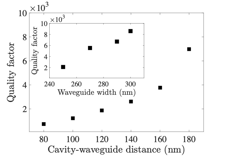 Figure 1
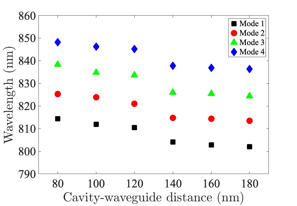 Figure 2
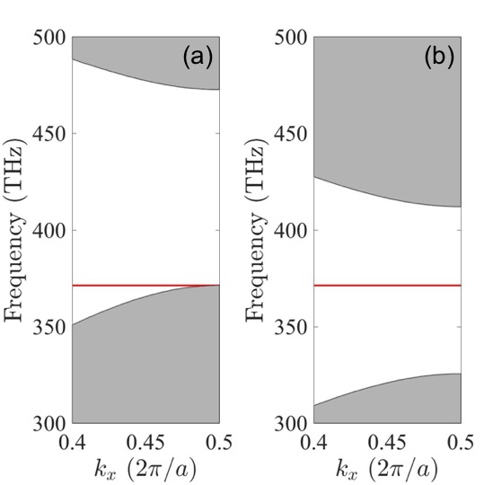 Figure 3
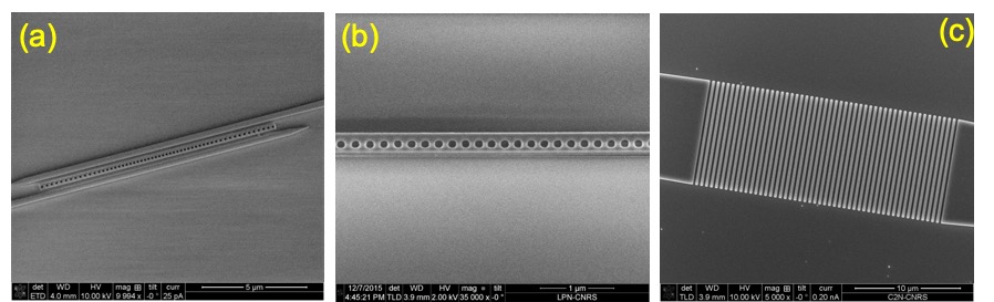 Figure 4
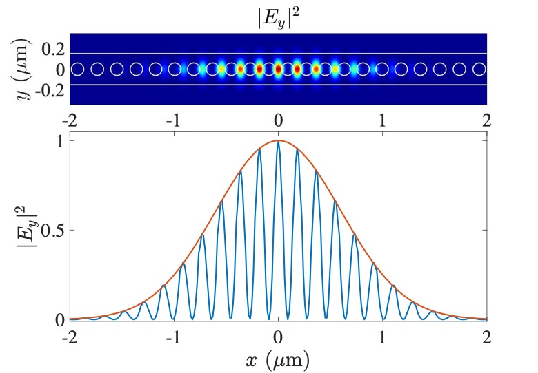 Figure 5
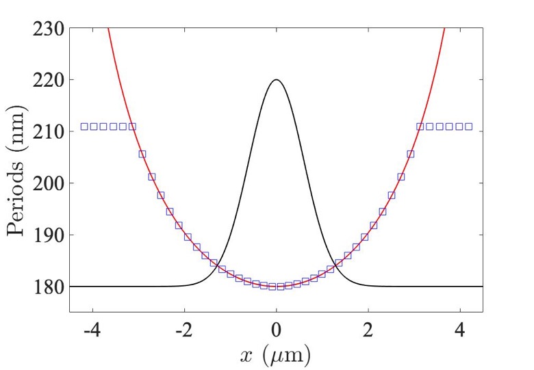 Figure 6
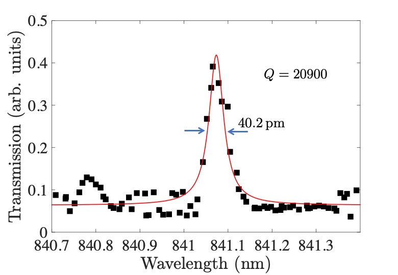 Figure 7
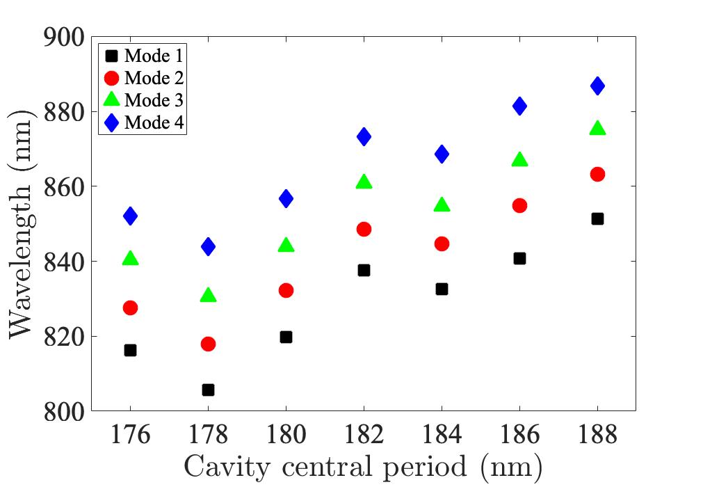 Figure 8
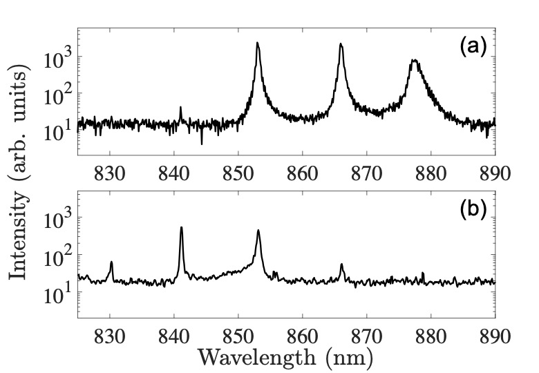 Figure 9
Peer Reviews
No public reviews on file for this paper yet. If you reviewed it on a platform where reviews are public (OpenReview, ICLR, NeurIPS, ICML), you can paste yours below so the community can read it here.
Videos
No videos yet. Explain this paper in a talk, walkthrough, or lecture? Add one.
Photonic crystal nanobeam cavities with optical resonances around 800 nm
I. Saber
Centre de Nanosciences et de Nanotechnologies CNRS/Université Paris-Saclay, 91120 Palaiseau, France
R. Boddeda
Laboratoire Kastler Brossel, Sorbonne Université, CNRS, ENS-PSL Research University, Collège de France, 4 place Jussieu, 75252 Paris, France
F. Raineri
Centre de Nanosciences et de Nanotechnologies CNRS/Université Paris-Saclay, 91120 Palaiseau, France
Université Paris Diderot, Sorbonne Paris Cité, 75013 Paris, France
D. Sanchez
Centre de Nanosciences et de Nanotechnologies CNRS/Université Paris-Saclay, 91120 Palaiseau, France
G. Beaudoin
Centre de Nanosciences et de Nanotechnologies CNRS/Université Paris-Saclay, 91120 Palaiseau, France
I. Sagnes
Centre de Nanosciences et de Nanotechnologies CNRS/Université Paris-Saclay, 91120 Palaiseau, France
Q. Glorieux
Laboratoire Kastler Brossel, Sorbonne Université, CNRS, ENS-PSL Research University, Collège de France, 4 place Jussieu, 75252 Paris, France
A. Bramati
Laboratoire Kastler Brossel, Sorbonne Université, CNRS, ENS-PSL Research University, Collège de France, 4 place Jussieu, 75252 Paris, France
J. A. Levenson
Centre de Nanosciences et de Nanotechnologies CNRS/Université Paris-Saclay, 91120 Palaiseau, France
K. Bencheikh
Centre de Nanosciences et de Nanotechnologies CNRS/Université Paris-Saclay, 91120 Palaiseau, France
Abstract
We report on the design and the fabrication of 1D photonic crystal (PhC) nanobeam cavities with optical resonances around 800 nm, compatible with Rubidium, Cesium or Argon atomic transitions. The cavities are made of Indium Gallium Phosphide (InGaP) material, a III-V semi-conductor compound which has a large index of refraction () favoring strong optical confinement and small mode volumes. Nanobeam cavities with inline and side coupling have been designed and fabricated, and quality factors up to have been measured.
††preprint: APS/123-QED
I Introduction
Cavity Quantum Electrodynamics (CQED) is based on the strong interaction between single atoms and photonsKimble1998 ; Walther2006 . The ability to reach this regime mostly relies in the possibility of confining the electromagnetic field in optical resonators with long-lived photons. Over the last years, impressive results have been achieved in terms of the figure of merit , by reducing the cavity dimensions and by improving the reflectivity of the constitutive mirrors. To obtain high factors with small mode volumes is one of the primary assets of Photonic Crystal (PhC) cavities. However, due to both technologic and application reasons, PhC are mostly developed at telecom wavelengths. Shorter wavelengths, suitable for example for strong coupling with cold atoms, are by far much more challenging in terms of technological accuracy Rousseau2017 .
Photonic crystal cavities are generally obtained by creating an optical defect in a structure with a periodic change in the refractive index distribution Yablonovitch1987 ; John1987 ; joannopoulos2011photonic . When the optical frequency of the electromagnetic field is in the band-gap of the PhC, light is trapped in the defect region Foresi1997 ; Joannopoulos1997 . Various cavities based on this principle have been designed and fabricated. Popular designs are based on 2D PhC, where one or several holes are removed from the otherwise periodic lattice Painter1819 ; Asano2006 ; Galli2014 or 2D PhC waveguides, where a full row of holes in the periodic lattice is removed Kuramochi2006 ; Asano2017 ; Noda2014 . In the latter, the cavity is obtained by engineering the period, largest in its center and decreasing when moving away. The propagating mode of the waveguide at the center becomes evanescent at the edges and is thus confined, forming a resonant mode. Cavities are also obtained in 1D PhC, usually made in a ridge waveguide in which two series of air-holes are etched Ahn2010 ; Halioua2010 ; Quan2010 ; Quan2011 ; Crosnier2016 . The two series are usually separated by a distance forming the cavity, where light is trapped. Such cavities, usually referred to as nanobeam cavities, benefit from the smallest mode volume and are thus of primary interest for CQED.
In this paper, we report on the design and fabrication of high PhC cavities with small mode volumes with optical resonances in the low infrared region (800 nm) which make them ideal to interact with alkali atoms such as Rubidium and Cesium and with Argon atoms. Our design is based on a typical 1D PhC cavity. However for a PhC with a fixed period, the achievable factors are quite limited. Indeed, the theory based on Fourier space analysis shows that the factors of the PhC cavities are limited by the out-of-plane scattering Vuckovic2002 ; Srinivasan2002 . To minimize the scattered power, one needs to attenuate the Fourier components in space below the light cone. This is obtained when the mode field has a Gaussian profile in real space Akahane2003 ; Akahane2005 ; Asano2006 . In practice, such mode profile can be achieved by engineering the PhC Bazin2014 ; Quan2011 throughout the modification of one or several of its parameters, namely the period, the hole radius, the width, or the thickness. In our design, we modulate only the PhC period along the propagation direction Bazin2014 . In order to reduce the cavity mode volume while minimizing the losses, our nanobeam cavities are designed in such a way that their length is a single period of the PhC, as demonstrated by Q. Quan et. al. in Ref. Quan2010 . The coupling into the nanocavity is an important issue to take into consideration when developing high- cavities. Indeed, as the unavoidable coupling opens an extra lossy channel, it will strongly influence the measured cavity factor. The coupling will also set the transmission amplitude to and from the cavity. The most trivial coupling way is the inline coupling, where the ridge waveguide in which the nanobeam cavity is made also serves as the input and output channels. Recently, it has been shown that in such design the transmission of the fundamental mode is rather lowAfzal2018 . This has been confirmed by our measurements and it is due to the wavevector mismatch between the resonant mode in the cavity and the propagating mode in the waveguide. In order to circumvent this transmission problem, we have also designed nanobeam cavities with side coupling. Ridge waveguides in the vicinity and on both sides of the nanobeam cavities are fabricated to couple in the light from a conventional laser source and to couple out the light from the cavities. To launch or extract light into the coupling waveguides, Bragg gratings are fabricated at their extremities as they are routinely used at telecom wavelengths Baets2006 . When properly designed, they could show extremely high coupling efficiencies Peucheret2013 ; Andreani2015 . However in this paper, we payed little attention to their design, focusing all our efforts on the development of the nanobeam cavities.
In the next section, we will first describe in detail the design to improve the factors of 1D PhC nanobeam cavities and present their fabrication process. The optical characterizations will be described in the last section, before the conclusion.
II Design and fabrication
In order to achieve nanobeam cavities with optical resonances close to 800 nm and small modal volumes, one needs to use a high-index compound transparent in the near infrared band. We have chosen Indium Gallium Phosphide (InGaP) because of its high index of refraction, at 800 nm, and its electronic band-gap of 1.85 eV which makes it transparent for wavelengths higher than 674 nm. The InGaP nanobeam is 150 nm thick, about , ensuring single mode operation, and 300 nm wide. The 1D PhC is obtained by etching 120 nm-diameter circular air-holes in the InGaP. For the factor optimization, the periods of the PhC were varied from 180 nm at the center to 215 nm at the edge of the nanobeam cavity, according to an algorithm that allows the mode to have a Gaussian shape, following the apodization technique described in Ref. Bazin2014 ; Akahane2003 . The algorithm gives the period as a function of the position in the PhC mirror. The out-of-plane losses are thus reduced by minimizing the scattered power given by the integral of the spatial Fourier components of the field within the light cone. Following the analysis in Ref. Bazin2014 , the first period is chosen in such a way that the target resonance frequency (THz, nm) of the cavity coincides with the cut-off frequency of the dielectric mode of the PhC at (). The field has an evanescent attenuation in the band-gap of the 1D PhC crystal, with an enveloppe decaying as where is the imaginary part of the wavevector.
At the cut-off frequency, attenuation constant is 0. Figure 1(a) shows the band diagram for 1D PhC with a period nm. The red line indicates the target resonance frequency and the gray regions are the dielectric (bottom) and air (top) bands of the PhC. The strongest value of is obtained for a PhC with a period nm, where lies in the middle of the band-gap as shown in Fig. 1(b). In order to have a field with a Gaussian profile, the attenuation needs to be varied linearly along the direction of the PhC, , so that the exponential decay becomes a Gaussian attenuation . Our algorithm allows to determine the evolution of the periods of the PhC from 180 nm to 215 nm along the direction to obtain a Gaussian field variation for a given full width at half maxima of the optical mode field, which depends on , the only free parameter. The continuous red line in Figure 2 shows the evolution of the period as a function of the position in the PhC mirror surrounding the cavity when the FWHM of the mode is chosen to be 1 m. The squares are the actual positions of the air-holes centers following the theoretical line. Additional air-holes, 5 in our case, with the maximal period are added at the end of the PhC mirrors in order to further increase the factor. The black line indicates the intensity profile of the Gaussian mode.
The optical properties of the designed InGaP nanobeam cavity are evaluated using three-dimensional Finite-Difference Time-Domain (3D FDTD) simulations implemented with LUMERICAL FDTD. We obtain a fundamental optical resonance at 811 nm, close to the target value, with a quality factor and a mode volume of 0.01 m3 which is about . The second and third-order modes are at 823 nm and 836 nm, and have respectively -factors of and with mode volumes and . Figure 3 shows the fundamental mode profile in the 2D plane of the cavity. The mode is mainly located between the air-holes in the dielectric as expected since we have fixed the target resonance frequency close to the dielectric band. The field intensity is maximum at the middle of the cavity where the period is nm. Moreover, it has a Gaussian envelope as indicated by the red line.
The nanocavities are fabricated by first growing InGaP on a GaAs substrate using metal-organic chemical vapor deposition. The InGaP/GaAs is then bonded to a Silicon on insulator Si/SiO2 substrate using benzocyclobutene (BCB) polymer layer. Finally the GaAs is removed using wet etching, obtaining thus the final 150 nm-thick InGaP layer on an SOI substrate. Electron-beam lithography is used afterwards to draw the designed PhC structures on the InGaP covered with a thin layer of electron-sensitive resist. After removing the non-exposed resist, the InGaP is etched using Inductively Coupled Plasma Reactive Ion Etching (ICP-RIE). Figure 4 shows Scanning Electron Microscope (SEM) images of typical nanobeam cavities we have fabricated: (a) with two adjacent waveguides intended for evanescent side coupling to the cavity; (b) with inline waveguide for direct coupling. Figure 4 (c) represents a SEM image of a typical grating fabricated at the extremities of the coupling waveguides. The Bragg gratings are used to couple in and out light to the waveguide from free space, usually from an optical fiber. The periodicity of the Bragg grating is 470 nm with a 50 % duty cycle, so that the diffraction angle is off the normal of the grating around nm in order to avoid back coupling into the fiber due to the second order diffraction. The Bragg gratings are fabricated simultaneously with the nanobeam cavity by fully etching the InGaP on half the period. The gratings are 10 m wide and 15 m long. For a lossless propagation from the grating couplers to the nanobeam cavity, a 300-m long optical taper is used between the 10-m large gratings and the narrow ( 300 nm) width coupling waveguides Fu2014 .
During the fabrication process, we have varied different parameters to study their effect on the optical properties of PhC. In the case of the inline nanobeam cavities, we varied the periods of the PhC to tune the wavelengths of the optical resonances. More specifically, we change the central period from 176 nm to 188 nm while keeping the maximal period at the edges at 215 nm. When increasing the period, the PhC band-gap is shifted towards lower energies. As a consequence, the resonant wavelengths, and more particularly the fundamental mode, are tuned to the red. For the nanobeam cavities with the side coupling strategy, we varied the width of the coupling waveguides and the distance between the cavity and the coupling waveguides. The parameters of the cavity, such as the central period of 180 nm and the maximal period of 215 nm, are kept constant. By construction, the nanobeam cavity and the coupling waveguides have identical thickness. When varying the width , the wavevector of the mode propagating in the coupling waveguides is tuned. The largest coupling to the cavity is obtained when matches with the wavevector of the fundamental resonant mode Crosnier2016 , i.e. . As the period of the PhC mirrors of the cavity is not constant, is determined by taking the Fourier transform of the mode represented in Fig. 3 (bottom sketch), obtaining nm. is achieved for a waveguide width nm. The distance between the nanobeam cavity and the coupling waveguide will modify the integral overlap between the mode field of the cavity and the mode field of the coupling waveguide. Both and will impact the coupling strength which can be quantified by an effective quality factor . The quality factor that will be measured experimentally is then given by , where is the intrinsic quality factor of the nanobeam cavity.
III Experimental observations
To investigate the fabricated nanobeam cavities, we used two laser sources. A pulsed Ti:Sapphire laser delivering 20-nm-width pulses at a repetition rate of 80 MHz and a continuous-wave (cw) diode laser source tunable between 790 nm and 850 nm. The pulsed source is used to identify rapidly the wavelengths of the resonances by analyzing the spectrum of the pulses out of the nanobeam cavities using a 40 pm resolution spectrometer (Ocean Optics HR2000). For the measurement of the resonance linewidths and hence the associated factors, we used the CW diode laser with a resolution of 1 pm. A wavelength-meter (Ångstrom WS6-600) with a measurement resolution of 20 MHz is used to read accurately the wavelength. To couple the light into the nanocavities we used a cleaved single mode fiber (Thorlabs 780HP), set at an incidence angle of about in front of the Bragg grating. The laser is coupled to the nanobeam cavity after diffracting from the Bragg grating and propagating along the optical taper and in the coupling waveguides. The transmitted light is collected using a long working distance microscope objective (Mitutoyo M Plan NIR 10) positioned above the output Bragg grating. We estimate the transmission to be about 0.04 %. It is inferred from the measurement of the power incident on the Bragg grating and the power collected after the microscope objective. The collected light is then coupled to a fiber and sent either to the spectrometer or to a high sensitivity Si photodiode.
When working with the inline nanobeam cavities, the transmission of the fundamental mode is weak and hard to observe. Figure 5 shows a typical spectrum measured with the spectrometer. In the spectrum of Fig. 5 (a), the light was collected at the output Bragg grating with the microscope objective. For this particular nanobeam cavity the fundamental mode is at 830 nm. However, due to the weakness of the coupling it is not observable. The first observable resonance is associated to the second-order mode at 841 nm as further shown in the spectrum of Fig. 5 (b) obtained by collecting directly the light leaking above the cavity. Note that in this case the fundamental mode although weak, is clearly observable. The weak transmission of the fundamental mode is due to the wavevector mismatch between the resonant mode and the mode propagating in the waveguide holding the nanobeam cavity which is 300 nm width. Furthermore, the spatial size of the fundamental mode along the propagation direction is very small (1 m FWHM) compared to the dimension of the nanobeam cavity as shown in Fig. 2. The resonant mode is thus strongly confined and hard to extract from the nanocavity. We did not succeed to measure the factor of the fundamental mode because of the weakness of signal, even when collecting it above the cavity. We have nevertheless measured the factor of the second-order mode at 841 nm using the cw laser. Figure 6 shows the obtained spectrum from which we can deduce a quality factor . According to the numerical FDTD simulations, the factor of the second-order mode is one order of magnitude smaller than that of the fundamental mode, we can thus expect a larger factor at 830 nm. However the measured factors are still below the numerical simulations by three to four orders of magnitude. This is a common trend when working with such very small dimensions PhC systems in which the propagating short-wavelength light becomes very sensitive to the surface imperfections. Indeed the cavity mode is not tightly confined in the so small cross-section of the nanobeam cavities. It is as well delocalized in the InGaP/SiO2 interface presenting surface roughness causing extra losses.
As expected, when increasing the central period of the inline nanobeam cavity, the wavelengths of the resonant modes are tuned, shifting to the infrared. This is indeed represented in Fig. 7 for the first four modes we have measured using the pulsed source and the spectrometer. The depicted resonances are obtained by measuring mainly the transmitted light collected at the output Bragg grating. Additional spectra obtained by measuring the cavity leakage were however necessary to confirm the wavelength of the fundamental mode. Similar measurements are done on the nanobeam cavities with the side coupling strategy. Figure 8 shows the first four modes measured using the pulsed laser source as a function of the cavity-waveguide distance. In the case of the side-coupled cavities, all the modes, and especially the fundamental one, are very well resolved.
The coupling waveguides have a width of 250 nm. As the coupling waveguide gets closer to the cavity, the wavelengths of the modes shift to the infrared. Indeed the nanobeam cavity’s effective index of refraction is altered, modifying the optical properties of the nanobeam cavity and hence its resonant wavelength. As the distance is increased, the coupling between the nanobeam cavity and the waveguide gets weaker, with negligible effects on the resonant modes. When the coupling waveguides are close to the nanobeam cavity, the transmission is higher. However the resonances become broader due to the large leakage which reduces the photons lifetime in the cavity. This is shown in Fig. 9 where the factor of the fundamental mode is plotted as a function of the distance for a waveguide width nm. The quality factors are deduced by measuring the FWHM of the resonances using the cw laser. We show also in the inset that the factor goes down as the width of the coupling waveguide is reduced. The quality factor should go down until nm is reached, width for which perfect phase matching is achieved between the resonant mode and the guided mode and hence optimum coupling. The best factor is below 10000 for the side coupled nanobeam cavities, a factor of two smaller than the factor of the inline nanobeam cavity. This is due to technological imperfections and the presence of extra coupling channels to the side waveguides.
IV Conclusion
In summary, we have proposed high- PhC nanobeam cavities with optical resonances at near infrared wavelengths around 800 nm, ideally suited for performing cavity QED-like measurements with alkali atoms.We have fabricated cavities using side and inline coupling. The best measured factor is about 20000. Though it is three orders of magnitude smaller than the predicted value, it is one of the highest factor measured at this short wavelength. We have shown that coarse tuning of the resonances can be easily achieved by a small change of the PhC parameters. Fine tuning can also be achieved by controlling the nanobeam cavities temperature.
Funding
Public grants CONDOR and ICQOQS overseen by the French National Research Agency (ANR) as part of the “Investissements d’Avenir” program (reference: ANR-10-LABX-0035, Labex NanoSaclay); French ANR grant UNIQ DS078; The French RENATCH Network and the French ANR grant UNIQ DS078.
Acknowledgment
The authors gratefully acknowledge Alejandro Giacomotti for helpful discussions.
The reference list from the paper itself. Each links out to its DOI / PubMed record.
- 1(1) H. J. Kimble, Phys. Scr. 1998 , 127 (1998).
- 2(2) H. Walther, B. T. H.Varcoe, B.-G. Englert, and T. Becker, Rep. Prog. in Phys. 69 ,1325 (2006).
- 3(3) I. Rousseau, I. Sánchez-Arribas, K. Shojiki, J.-F. Carlin, R. Butté, and N. Grandjean, Phys. Rev. B 95 , 125313 (2017).
- 4(4) E. Yablonovitch, Phys. Rev. Lett. 58 , 2059 (1987).
- 5(5) S. John, Phys. Rev. Lett. 58 , 2486 (1987).
- 6(6) J. Joannopoulos, S. Johnson, J. Winn, and R. Meade, Photonic Crystals: Molding the Flow of Light , Second Edition (Princeton University Press, 2011).
- 7(7) J. S. Foresi, P. R. Villeneuve, J. Ferrera, E. R. Thoen, G. Steinmeyer, S. Fan, J. D. Joannopoulos, L. C. Kimerling, H. I. Smith, and E. P. Ippen, Nature 390 , 143 (1997).
- 8(8) J. D. Joannopoulos, P. R. Villeneuve, and S. Fan, Nature 386 , 143 (1997).