A symmetry-derived mechanism for atomic resolution imaging
Matus Krajnak, Joanne Etheridge

TL;DR
This paper presents a novel symmetry-based contrast mechanism for STEM that enhances atomic resolution imaging by leveraging local symmetry, providing sharper atomic columns and complementing existing imaging modes.
Contribution
A new symmetry-derived contrast mechanism for STEM that improves atomic resolution imaging and is robust across various experimental conditions.
Findings
Detects both light and heavy atomic columns
Produces sharper atomic peaks than conventional methods
Can be acquired simultaneously with existing imaging modes
Abstract
We introduce a new image contrast mechanism for scanning transmission electron microscopy (STEM) that derives from the local symmetry within the specimen. For a given position of the electron probe on the specimen, the image intensity is determined by the degree of similarity between the exit electron intensity distribution and a chosen symmetry operation applied to that distribution. The contrast mechanism detects both light and heavy atomic columns and is robust with respect to specimen thickness, electron probe energy and defocus. Atomic columns appear as sharp peaks that can be significantly narrower than for STEM images using conventional disc and annular detectors. This fundamentally different contrast mechanism complements conventional imaging modes and can be acquired simultaneously with them, expanding the power of STEM for materials characterisation.
Click any figure to enlarge with its caption.
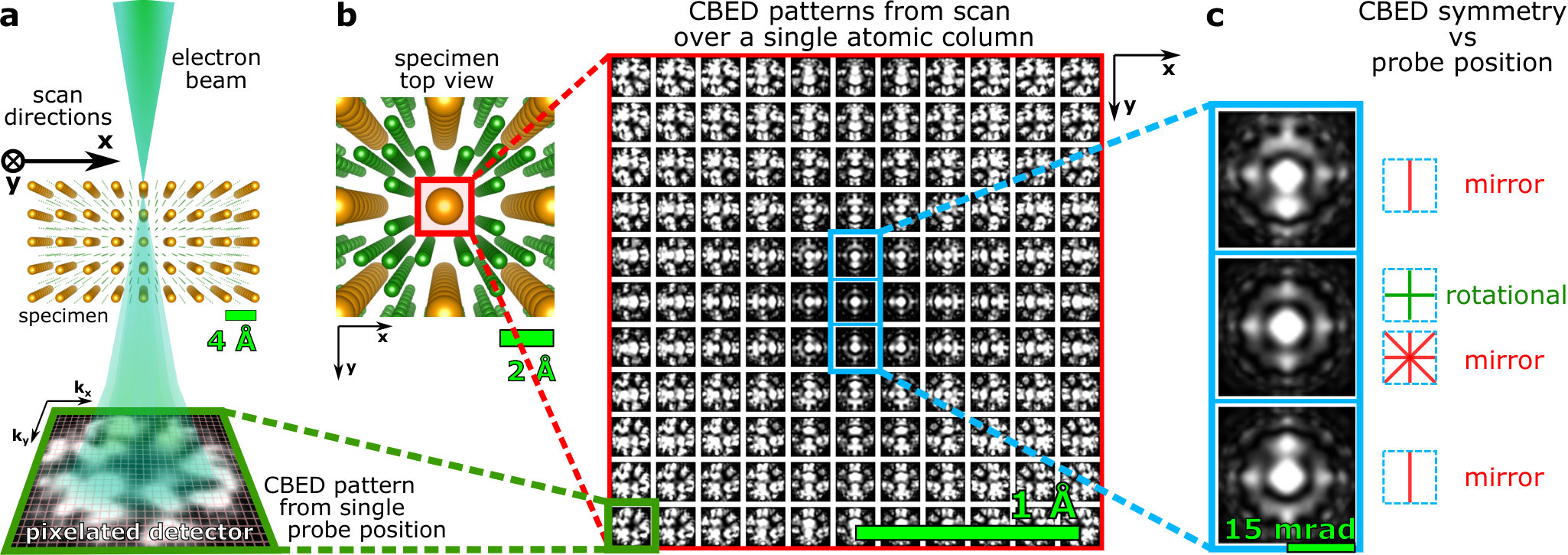 Figure 1
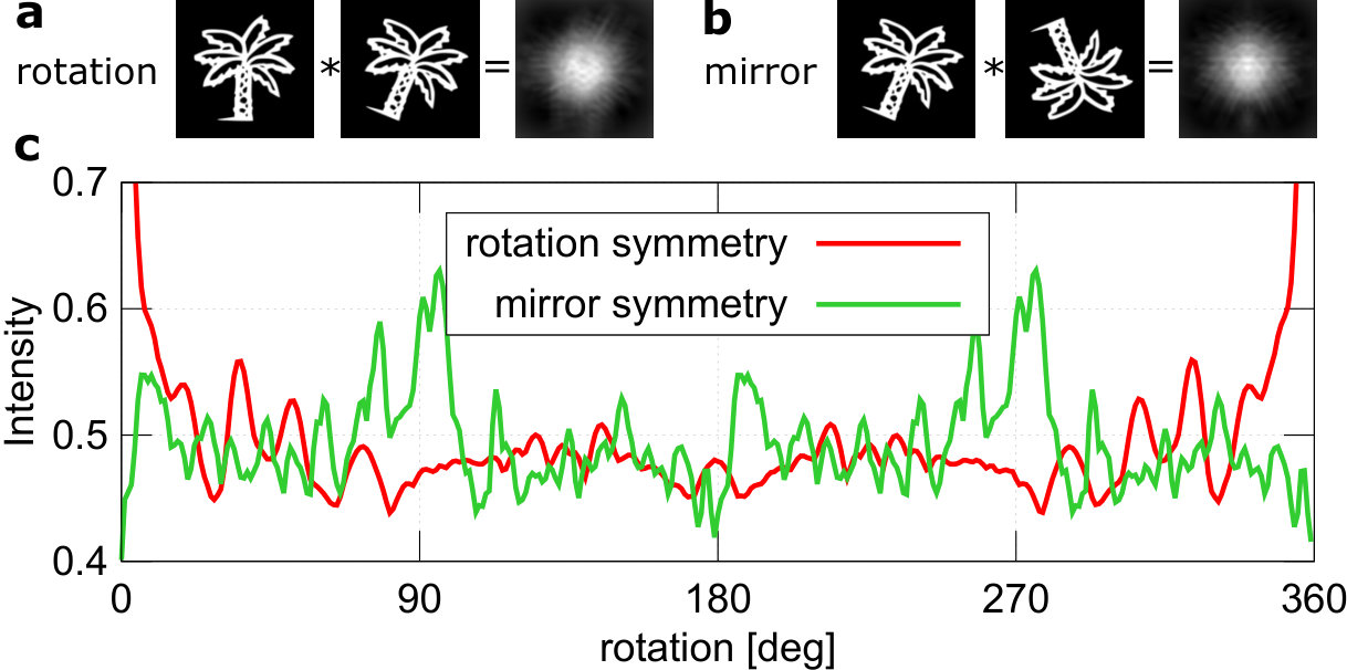 Figure 2
 Figure 3
 Figure 4
 Figure 5
Peer Reviews
No public reviews on file for this paper yet. If you reviewed it on a platform where reviews are public (OpenReview, ICLR, NeurIPS, ICML), you can paste yours below so the community can read it here.
Videos
No videos yet. Explain this paper in a talk, walkthrough, or lecture? Add one.
A symmetry-derived mechanism for atomic resolution imaging
Matus Krajnak1,2 and Joanne Etheridge1,3
1Department of Materials Science and Engineering, Monash University, Victoria 3800, Australia
2Current address: Quantum Detectors Ltd, R104 RAL, Harwell Oxford OX11 0QX, UK
3Monash Centre for Electron Microscopy, Monash University, Victoria 3800, Australia
\StrLeft
We introduce a new image contrast mechanism for scanning transmission electron microscopy (STEM) that derives from the local symmetry within the specimen. For a given position of the electron probe on the specimen, the image intensity is determined by the degree of similarity between the exit electron intensity distribution and a chosen symmetry operation applied to that distribution. The contrast mechanism detects both light and heavy atomic columns and is robust with respect to specimen thickness, electron probe energy and defocus. Atomic columns appear as sharp peaks that can be significantly narrower than for STEM images using conventional disc and annular detectors. This fundamentally different contrast mechanism complements conventional imaging modes and can be acquired simultaneously with them, expanding the power of STEM for materials characterisation.1[\firstletter] \firstletter\StrGobbleLeftWe introduce a new image contrast mechanism for scanning transmission electron microscopy (STEM) that derives from the local symmetry within the specimen. For a given position of the electron probe on the specimen, the image intensity is determined by the degree of similarity between the exit electron intensity distribution and a chosen symmetry operation applied to that distribution. The contrast mechanism detects both light and heavy atomic columns and is robust with respect to specimen thickness, electron probe energy and defocus. Atomic columns appear as sharp peaks that can be significantly narrower than for STEM images using conventional disc and annular detectors. This fundamentally different contrast mechanism complements conventional imaging modes and can be acquired simultaneously with them, expanding the power of STEM for materials characterisation.1
In scanning transmission electron microscopy (STEM), images can be generated by scanning an electron beam across the object and, at each position of the electron beam, detecting the scattered electron intensity distribution after transmission through the specimen. The most common STEM imaging modes integrate the scattered intensity in the diffraction plane across a particular angular range, using either disc or annular detector geometries, to generate phase-contrast Bright Field (BF) and adsorptive-contrast High Angle Annular Dark Field (HAADF) images, respectively, (or a mix of phase and adsorptive contrast in the case of Annular Bright Field (ABF)). Recently, the advent of fast read-out, high dynamic range detectors [1, 2, 3, 4, 5, 6] has enabled the full angular distribution of scattered intensity to be recorded at each beam position. This represents a revolution in STEM, providing access to a vast and rich palate of additional specimen information [7]. Fast detectors have already been applied, for example, to improve STEM spatial resolution using ptychography [8, 9, 10, 11, 12], to map electric [13, 14] and magnetic fields [15, 4, 16, 17, 18], strain [11, 19, 20, 21, 18], polarization domains [22], and octahedral tilts [23], representing just the beginning of this powerful new era in STEM.
Here we propose a new image contrast mechanism for atomic resolution STEM based on a measurement of the degree of symmetry in the scattered intensity distribution at each point of a scan: Symmetry STEM (S-STEM). By virtue of the strong electron-specimen interaction and resultant dynamical scattering, the symmetry of the illuminated specimen volume is encoded in the symmetry of the scattered intensity distribution, independent of the specimen thickness and accelerating voltage [24, 25, 26, 27]. In this paper, the scattered intensity distribution is in the form of a convergent beam electron diffraction (CBED) pattern (Fig. 1a), the most common case for STEM [28], but the approach can be applied in principle to any form of scattered intensity distribution in any optical plane and also to other scanning microscopy techniques.
The ‘degree’ of symmetry in a pattern can be analysed by a comparison of the scattered intensity distribution with itself after an applied symmetry operation [29]. For a given two dimensional (2D) pattern , the symmetry intensity is given by:
[TABLE]
where is a normalised cross-correlation and the symmetry operation can be chosen (for example, a rotation or a mirror). If is invariant under the symmetry operation, then the intensity will be maximum, , and if the symmetry is not matched. Analogous algorithms have been applied to visualise biological macromolecules [30, 31] and in measurements of local polarization domains [32, 33]. Here, our goal is different, namely, to deliver an image contrast mechanism that derives from spatial variations in symmetry, measured at picometre intervals.
In the case of Symmetry STEM, the intensity will be calculated from each CBED pattern at each point of a 2D scan, , which can be plotted as an image . Each CBED pattern resolves the electron distribution in reciprocal space at a particular point, , of a scan , denoting one point in a so called four dimensional (4D) STEM dataset [34]. Data processing was based on methodology introduced in Refs. [15, 35, 36] and implemented in GPU accelerated ArrayFire library [37]. The application of Equation 1 to 4D-STEM dataset generates an entirely different image contrast mechanism, neither phase-contrast nor adsorption-contrast, which provides access to new specimen information at the atomic level.
Results
Calculations
The sensitivity to local symmetry that underpins the Symmetry STEM contrast mechanism is illustrated with a STEM simulation on a test case, \ceCeB6. \ceCeB6 has both small (B-B : ), and large (Ce-Ce : ) column spacings and comprises light (B = 5) and heavy (Ce = 58) atoms, which are challenging to image simultaneously in BF or ADF STEM. Figure 1b shows an array of simulated CBED patterns corresponding to a FWHM probe scanning across the \ceCe column in oriented \ceCeB6. Each simulated CBED pattern is arranged according to the corresponding real space position, , of the probe, with the \ceCe column position centred at the centre of the array. The GPU accelerated parallel implementation of the multislice simulations were performed using the Prismatic software package [38, 39, 40] using parameters described in Methods - STEM simulation. The arranged CBED patterns give a clear sense of how the symmetry changes as the probe is scanned across the \ceCe atomic column in steps (Fig. 1c). For example, there is an immediate shift from 4-fold and multiple mirrors (4mm) to a single mirror symmetry (m) as the probe centre moves from the absolute centre of the atomic column to just picometres off-centre (but is nevertheless still located on the atomic column). This highlights the acute sensitivity to local specimen symmetry that is delivered by dynamical scattering [25, 26, 27, 41] and forms the basis of image contrast in Symmetry STEM.
Equation 1 provides an extremely efficient method for distilling the local symmetry information present in the pattern. This is illustrated generically in Fig. 2 for an intensity distribution, , in the form of a palm tree. Two classes of symmetry are tested, a rotation and mirror symmetry. These symmetry operations can be tested for an arbitrary angle on this arbitrary pattern, (e.g. Figs. 2a and 2b, test a rotation for the palm tree pattern). The cross-correlation is calculated for to (Fig. 2c). It can be seen that even if the pattern does not possess a perfect symmetry element, there still exist local maxima in the analysis. For the palm tree pattern this signal arises when the leaves are overlapping after application of a given symmetry operation. It should be noted that only to angles need to be calculated because only the relative rotation matters. clockwise and anti-clockwise rotations have the same maximum of cross-correlation (ignoring interpolation errors). For additional notes about this symmetry analysis please see Supplementary information.
To demonstrate Symmetry STEM, the symmetry analysis of Eq. 1 will now be applied to the simulated scanning CBED dataset (Fig. 1) across a field of view slightly larger than a \ceCeB6 unit cell (Fig. 3a), again using the parameters described in Methods - STEM simulation. Symmetry STEM images corresponding to rotation, mirror and rotation are generated (Figs. 3b-d, respectively). For comparison, standard STEM BF, ABF and HAADF images were also reconstructed (Figs. 3e-g, respectively) by integrating across the angular ranges indicated in (Fig. 3h) for each probe position.
As anticipated, the S-STEM images exhibit atomic-scale contrast, revealing local maxima wherever some degree of the applied symmetry element is present, reaching a maximum value near one when there is an identity, such as on the \ceCe column at rotation and mirror. rotation symmetry shows exceptionally intense and sharp contrast for \ceCe, small local maxima at all \ceB positions, and also it highlights the symmetry with a broad maxima half way between \ceCe atomic columns along (Fig. 3b). mirror symmetry shows bright contrast where mirror planes within the lattice match the symmetry (Fig. 3c). An interesting contrast arises when a small rotation symmetry of is measured (Fig. 3d) giving extra sensitivity to the rate of change of the local symmetry. Strong ‘intensity’ appears where the CBED pattern is rotationally symmetric or it varies slowly with angle , namely at the position of asymmetric \ceB atom sites, with weak intensity at the \ceCe sites where the pattern varies rapidly.
Importantly, local maxima at atomic sites in the Symmetry STEM images are exceptionally sharp with low intensity ‘moats’ around them. This is particularly the case for the peaks at \ceCe columns with a FWHM of \sim$$0.25\text{\,}\mathrm{\SIUnitSymbolAngstrom} (Fig. 3i), which are significantly narrower than the peaks in the corresponding conventional BF, ABF and HAADF STEM images (using a diffraction limited probe with FWHM (Fig. 3i)). Local maxima due to the presence of a symmetry element but in the absence of an atomic column do not show the ‘moat’ because the rate of change of specimen symmetry is more slowly varying than in the presence of an atomic column. This enables atom sites to be distinguished from atom-free symmetry sites. This distinction can be further checked when S-STEM images derived from different symmetry elements are compared.
We examine further the imaging properties of Symmetry STEM by calculating a line scan over \ceCe-B-Ce atomic columns in \ceCeB6 for different defocus and probe size and sample thickness and tilt (Fig. 4). The symmetry element is chosen to be a rotation and the base parameters are as specified in Methods - STEM simulations and kept constant unless otherwise noted. For comparison, we have also calculated the corresponding BF, ABF and ADF STEM line scans (Supplementary Fig. S1).
Dependence on Thickness and Defocus: As S-STEM probes local symmetry within the sample, the contrast does not change at the centre of atomic sites due to the change of defocus nor thickness (Figs. 4a and b respectively). This is a consequence of the fact that, while the scattered intensity distribution can vary rapidly with thickness, accelerating voltage and defocus, its’ symmetry remains invariant. This is a great advantage over standard methods for which the sign and magnitude of the signal can change. For all thicknesses, the intensity peaks at atomic sites are an almost constant, extremely narrow width (\sim$$0.25\text{\,}\mathrm{\SIUnitSymbolAngstrom}), with some local variations in the vicinity of the \ceB octahedra likely due to scattering onto nearby high symmetry sites. Nevertheless, even in the presence of this “cross-talk”, the narrow peak persists (inset Fig. 4b).
Resolution and Probe size: Symmetry-STEM is an example of a “two-step” imaging system (as defined by Gureyev and Paganin et al in Refs. [42, 43]) with resolution a consequence of both the experimental system and the virtual post-processing (see Supplementary information). The sharpness of an intensity maxima and consequent ability to resolve two features in S-STEM depends on the ability of the probe to detect a symmetry change. In other words, it depends on the probe size relative to the rate of change with position of the symmetry of the local specimen potential. The resolution of Symmetry STEM images is therefore only a function of the direct electron-optical imaging system in so far as this system defines a probe size (which is set by the collective effect of the spatial coherence function, probe-forming aberrations and aperture size [44]).
In the aberration-free, spatially coherent calculations, the convergence semi-angle defines the probe size and was varied from – (Fig. 4c). The signal is constant and identity at ( probe FWHM) because the probe is greater than the unit cell in this perfect crystal, so no change in symmetry can be detected. Put another way, the CBED patterns have non-overlapping CBED discs and hence do not change with position.
From the calculations, it can be seen that when the convergence semi-angle () generates a probe FWHM () comparable to the atomic radius (\sim$$2.35\text{\,}\mathrm{\SIUnitSymbolAngstrom} van de Waals) we start to resolve clearly the two \ceCe columns. With higher convergence (\sim$$7\text{\,}\mathrm{m}\mathrm{r}\mathrm{a}\mathrm{d}), the probe FWHM (\sim$$1.7\text{\,}\mathrm{\SIUnitSymbolAngstrom}) approaches two thirds of the atomic radius and the image peaks sharpen significantly to \sim$$0.4\text{\,}\mathrm{\SIUnitSymbolAngstrom} FWHM (Fig. 4c, compared with \sim$$1.3\text{\,}\mathrm{\SIUnitSymbolAngstrom} FWHM for the corresponding image peaks in BF-, ABF-, ADF-STEM images in Supplementary Fig. S2b,c and d). This trend continues to \sim$$22\text{\,}\mathrm{m}\mathrm{r}\mathrm{a}\mathrm{d}, where the probe FWHM is , less than a quarter of the atomic radius. Here the image peak width is <$$0.2\text{\,}\mathrm{\SIUnitSymbolAngstrom}, which is half of the diffraction-limited probe size set by this convergence angle and a fifth of the image peak width for conventional BF-, ABF- and ADF-STEM modes (Supplementary Fig. S2b,c and d). The sharpness of the peak reduces for convergence angles larger than \sim$$25\text{\,}\mathrm{m}\mathrm{r}\mathrm{a}\mathrm{d}, possibly due to scattering onto nearby atomic sites promoted by the larger transverse momentum of the incident probe.
Dependence on Tilt: Tilt of a sample is a crucial parameter to study as it changes the excitation errors and hence the symmetry of the scattering matrix and resulting CBED pattern. The sample was tilted from the zone axis by to in the plane of the line scan (Fig. 4d). When the sample is tilted more than the symmetry peak related to \ceCe starts to disappear, while the \ceB peak broadens but persists (likely due to the \ceB octahedra acting effectively as a single scatterer). In some crystalline specimens, this sensitivity to tilt could be helpful for the precise alignment of the crystal along a zone axis, without the problem of significant defocus change with tilt (Fig. 4a).
Experiment
Finally, we compare the Symmetry STEM analysis of simulated data with experimental data from \ceCeB6 (Fig. 5). The scanned CBED data was collected at on an early generation double-spherical aberration corrected FEI Titan3 80–300 FEGTEM equipped with a pixelated EMPAD detector [4]. Aberrations were largely corrected within the convergence semi-angle of . Conventional BF and ABF STEM images were reconstructed (Fig. 5a and b, respectively) to compare with the Symmetry STEM signals with the same symmetry operations as applied in Fig. 3 (Fig. 5). (The HAADF signal was not collected here because the large angular field of view required would constrain the symmetry measurement from the central disk area.) The and rotation images (Figs. 5d and e, respectively), show contrast closely related to the theoretical calculations (Fig. 3). In particular, the rotation image shows extremely sharp peaks surrounded by dark ‘moats’, corresponding to the symmetry maxima when the probe is positioned at the absolute centre of the \ceCe atomic column and the break of symmetry as soon as the beam shifts slightly from the centre but remains on the column, as seen in the calculations (Fig. 3f). We can also see the symmetric position of the central \ceB atomic column, however the asymmetric sites of other \ceB atomic positions are not as clear, most likely due to imperfect instrument and specimen stability and a lack of local rotation symmetry in the position. The rotation image shows very strong signal to noise at the \ceCe columns and also shows some residual specimen tilt effects. An average unit cell image (from five unit cells) is compared with the calculated image in Fig. 5f.
Discussion
In Symmetry STEM, the symmetry of the local specimen potential defines the mathematical symmetry of the dynamical N-dimensional scattering matrix [25, 26, 27] and this, in turn, defines the symmetry of the scattered intensity distribution (CBED pattern) which is extracted using Equation 1, providing an intrinsically different image contrast mechanism.
For perfect crystals, a reduction in symmetry can be detected as soon as an atomic-scale probe shifts a few picometres from the centre of an atomic column. Our calculations show this can generate extremely sharp image peaks at atomic column positions (Fig. 3i) that have smaller FWHM than the corresponding peaks/troughs in conventional diffraction-limited BF-, ABF- and ADF-STEM images derived from the same 4D-STEM data set (see Figs. 4i and Supplementary S4).
For unknown structures, the presence of a mirror or any point symmetry element can be detected through the automated application of the Symmetry STEM algorithm (Equation 1) for any rotation angle, as illustrated in Figure 2 and the Movies S1 and S2. Similarly, this can enable defects, which break local symmetry, to be highlighted.
In experimental data, the practical limit is the stability of the instrument and specimen, collectively ‘scan noise’. The proof-of-concept examples in Fig. 5 were taken on a decade-old instrument. The on-going improvements in instrument stability and detector speeds bode well for the further development of this technique. The remarkable robustness of S-STEM images to thickness, accelerating voltage and defocus is because the mathematical symmetry of the scattering matrix and hence the CBED pattern symmetry does not depend on these quantities. The acute sensitivity to tilt is because it does. The latter provides an opportunity for an automated, high precision tilt alignment [45]. The potential of Symmetry STEM to obtain atomic resolution images of light and heavy atoms, from thick and thin crystals across a wide selection of accelerating voltages opens up a range of applications in material science that are otherwise challenging to image, including thick and beam sensitive specimens. The ability to image defects due to the change in symmetry they induce, also opens new opportunities, including the imaging of dopant atoms and dislocations. The method could also be applied to the imaging of atomic magnetic fields in electromagnetic circular dichroism [46]. Furthermore, Symmetry STEM is likely to be sensitive to atomic displacements which induce a local change in symmetry, such as can occur with strain or octahedral tilts.
Methods
STEM imaging
Imaging was performed using a double- spherical-aberration corrected Titan3 80-300 FEG-TEM equipped with an EMPAD pixelated detector[4] and operating at electron energy with a probe convergence semi-angle. The dataset was a 4D-STEM data of 128x128 probe positions with the size 1GB.
Symmetry analysis
A custom made C++ code using GPU accelerated library ArrayFire [37] was used to analyse symmetry in two dimensional diffraction pattern images. A maximum value of a normalised cross(phase)-correlation for a specific symmetry operation is plotted for each point of a scan.
STEM simulations
Prismatic software package [38, 39] was used to simulate 4D-STEM datasets. The parameters were: \ceCeB6 sample was (Fig. 1) or (Figs. 3 and 4) thick, in orientation, convergence semi-angle was , acceleration voltage , slice thickness was , beam was focused on the top surface and no aberrations were used. The size of a single dataset was and included 124x124 probe positions.
Acknowledgements
We thank Prof. David Paganin for helpful comments on the manuscript and A/Prof Matthew Weyland for helpful suggestions for STEM alignment. We thank Dr Ding Peng and A/Prof Philip Nakashima for the tripod polished \ceCeB6 specimen from a crystal supplied by Mr. P. Hanan via Prof AWS Johnson [47]. This work was supported by the Australian Research Council (ARC) grant DP150104483 and used instruments at the Monash Centre for Electron Microscopy funded by ARC grant LE0454166.
The reference list from the paper itself. Each links out to its DOI / PubMed record.
- 1[1] Battaglia, M. et al. Characterisation of a CMOS active pixel sensor for use in the TEAM microscope. Nuclear Instruments and Methods in Physics Research Section A: Accelerators, Spectrometers, Detectors and Associated Equipment 622 , 669–677 (2010).
- 2[2] Ballabriga, R. et al. Medipix 3: A 64 k pixel detector readout chip working in single photon counting mode with improved spectrometric performance. Nuclear Instruments and Methods in Physics Research Section A: Accelerators, Spectrometers, Detectors and Associated Equipment 633 , S 15–S 18 (2011).
- 3[3] Ryll, H. et al. The pn CCD for applications in transmission electron microscopy: Further development and new operation modes. Microscopy and Microanalysis 20 , 1122–1123 (2014).
- 4[4] Tate, M. W. et al. High dynamic range pixel array detector for scanning transmission electron microscopy. Microscopy and Microanalysis 22 , 237–249 (2016).
- 5[5] Mir, J. et al. Characterisation of the Medipix 3 detector for 60 and 80 ke V electrons. Ultramicroscopy 182 , 44–53 (2017).
- 6[6] Faruqi, A. & Mc Mullan, G. Direct imaging detectors for electron microscopy. Nuclear Instruments and Methods in Physics Research Section A: Accelerators, Spectrometers, Detectors and Associated Equipment 878 , 180–190 (2018).
- 7[7] Ophus, C. Four-dimensional scanning transmission electron microscopy (4D-STEM): From scanning nanodiffraction to ptychography and beyond. Microscopy and Microanalysis 25 , 563–582 (2019).
- 8[8] Pennycook, T. J. et al. Efficient phase contrast imaging in STEM using a pixelated detector. Part 1: Experimental demonstration at atomic resolution. Ultramicroscopy 151 , 160–167 (2015).