Calculating the Band Structure of 3C-SiC Using sp3d5s*+$\Delta$ Model
Murat Onen, Marco Turchetti

TL;DR
This paper develops a semi-empirical tight binding model incorporating sp3d5s* orbitals and spin-orbit coupling to accurately calculate the band structure of 3C-SiC, validated against experimental data.
Contribution
It introduces a detailed method for creating a tight binding model for zincblende semiconductors using Slater-Koster integrals, with an optimization process for experimental accuracy.
Findings
High accuracy in band diagram evaluation
Effective mass calculations match experimental results
Model successfully reproduces energy levels at high symmetry points
Abstract
We report on a semi-empirical tight binding model for 3C-SiC including the effect of sp3d5s* orbitals and spin-orbital coupling. In this work, we illustrate in detail the method to develop such a model for semiconductors with zincblende structure, based on Slater-Koster integrals, and we explain the optimization method used to fit the experimental results with such a model. This method shows high accuracy for the evaluation of 3C-SiC band diagram both in terms of the experimental energy levels at high symmetry points and the effective masses.
Click any figure to enlarge with its caption.
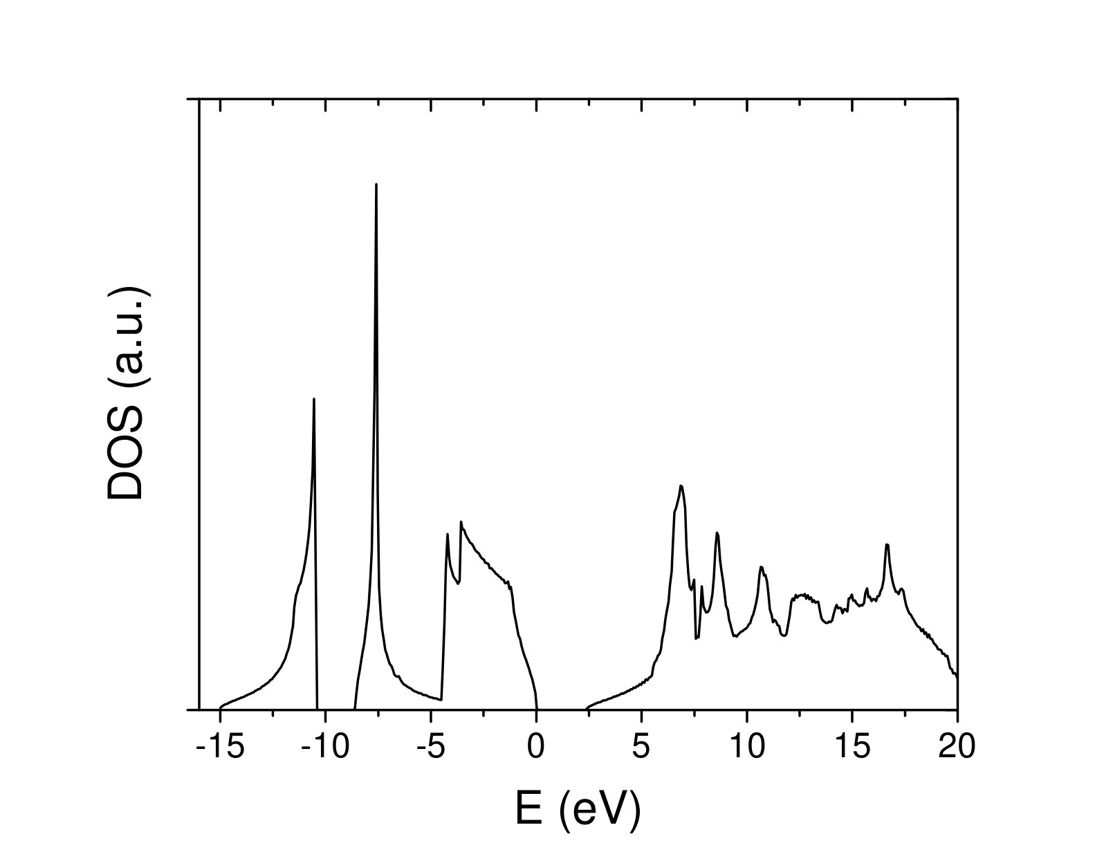 Figure 1
 Figure 2
 Figure 3
 Figure 4
 Figure 5
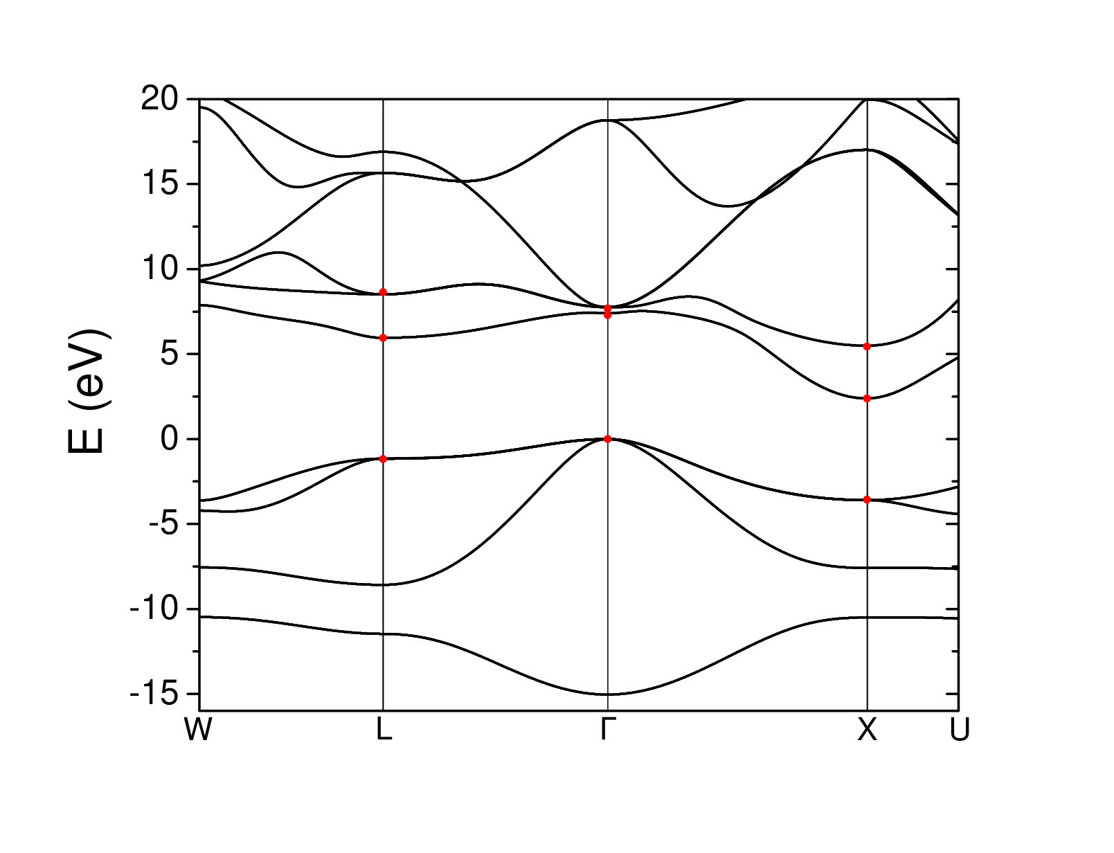 Figure 6
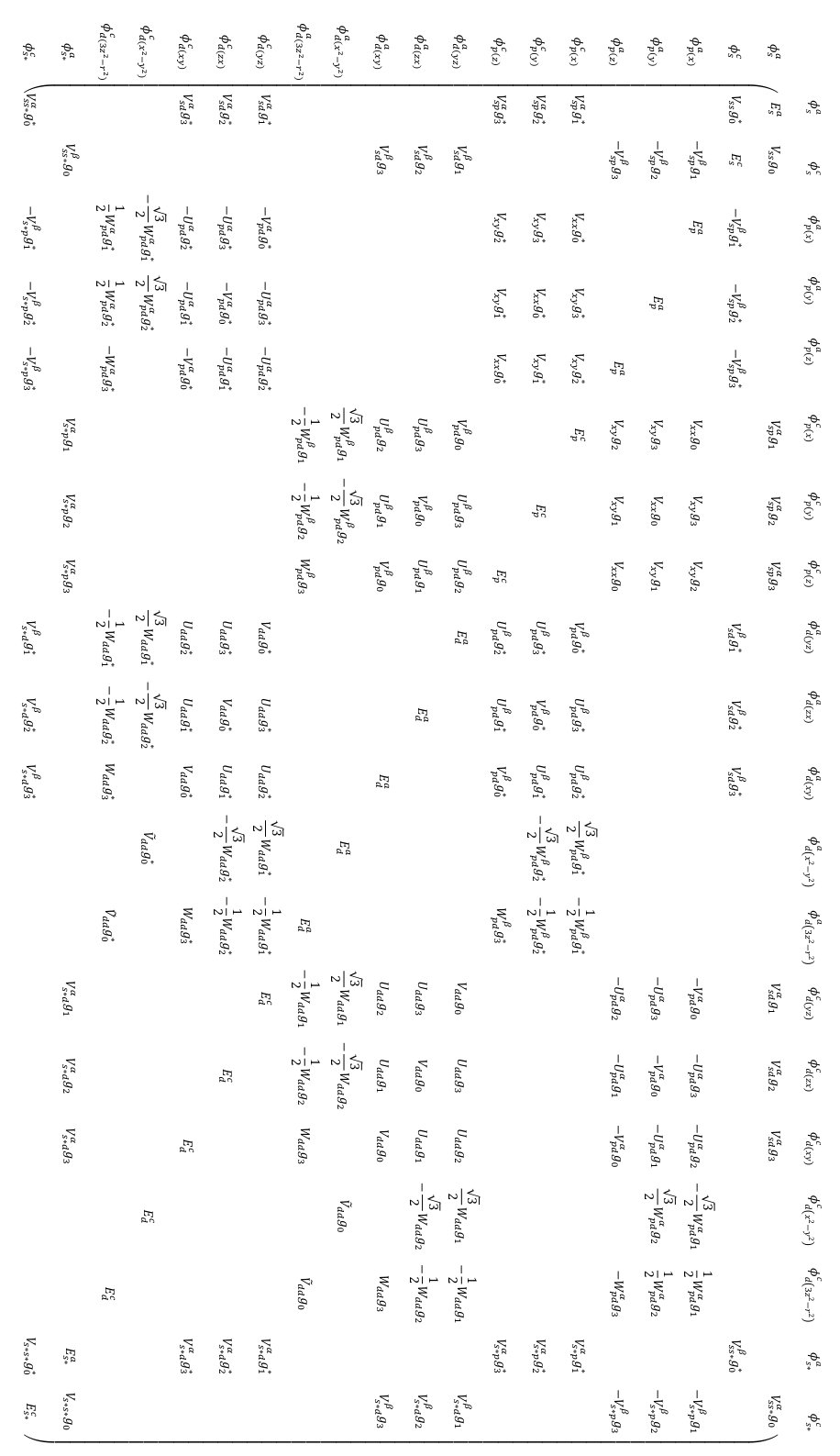 Figure 7
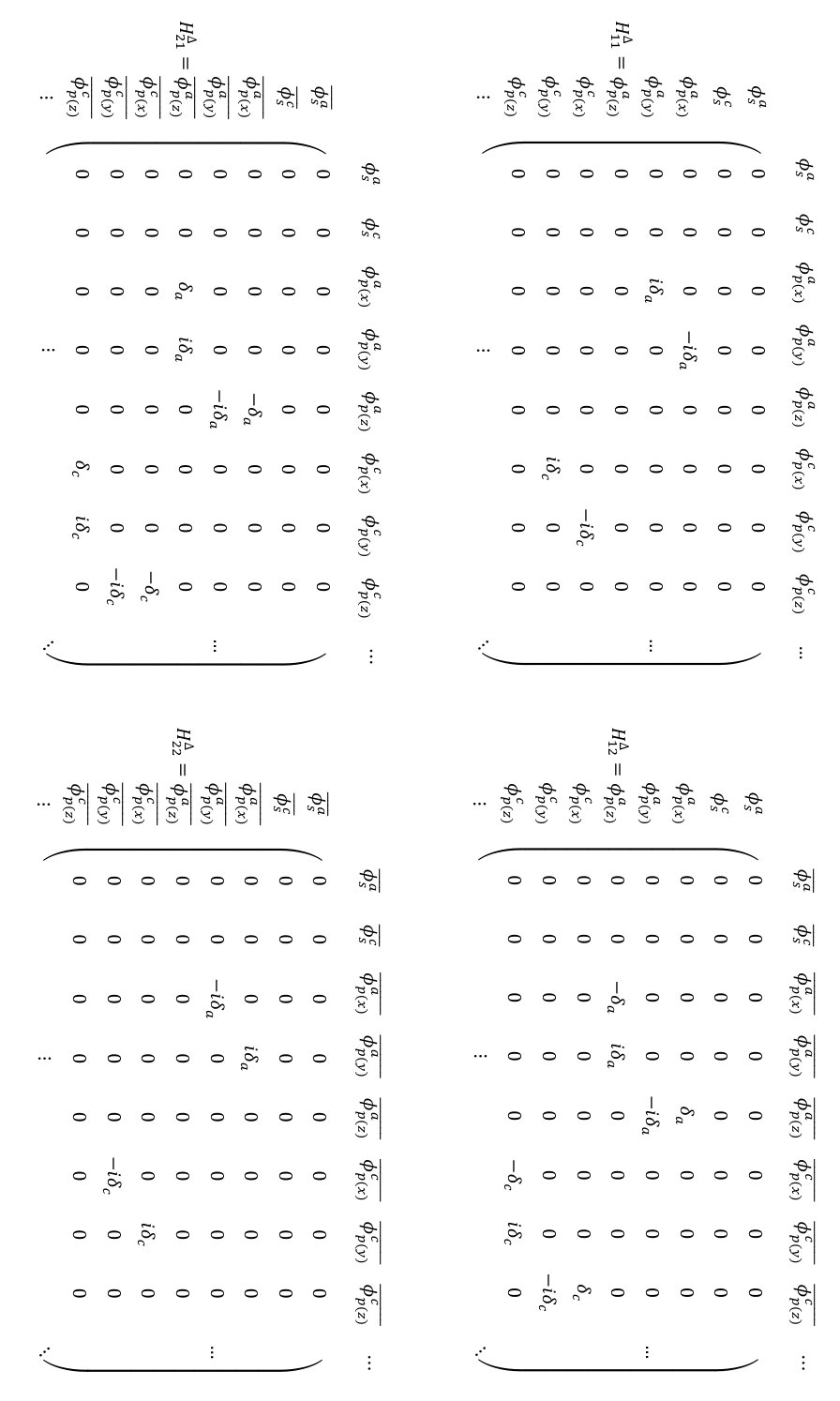 Figure 8
| Parameter | GaAs | SiC |
|---|---|---|
| a | 5.6532Å | 4.3596 Å |
| -6.0533 | -0.8766 | |
| -0.3340 | -0.3421 | |
| 3.3063 | 0.5489 | |
| 6.2866 | 5.4488 | |
| 13.3395 | 22.9218 | |
| 13.3327 | 14.7797 | |
| 19.3982 | 21.4411 | |
| 19.3982 | 24.3075 | |
| -1.7167 | -1.9875 | |
| -3.9205 | -1.5826 | |
| -2.1479 | -6.9155 | |
| -1.3658 | -0.7085 | |
| 2.6999 | 5.6044 | |
| 2.9036 | 4.6564 | |
| 2.2556 | 6.5528 | |
| 2.5823 | 5.0141 | |
| -2.7144 | -6.5282 | |
| -2.4623 | -4.3586 | |
| -0.6651 | -0.2985 | |
| -0.5404 | -0.3126 | |
| 4.3807 | 6.9700 | |
| -1.3874 | -2.2015 | |
| -1.3147 | -3.9538 | |
| -1.5263 | -6.0081 | |
| 2.1184 | 1.4686 | |
| 2.4926 | 3.1505 | |
| -0.7282 | -1.1553 | |
| 1.6289 | 4.4417 | |
| -1.8121 | -4.9623 | |
| 0.1630 | 0.0071 | |
| 0.0823 | 0.0030 |
Peer Reviews
No public reviews on file for this paper yet. If you reviewed it on a platform where reviews are public (OpenReview, ICLR, NeurIPS, ICML), you can paste yours below so the community can read it here.
Videos
No videos yet. Explain this paper in a talk, walkthrough, or lecture? Add one.
Taxonomy
TopicsSilicon Carbide Semiconductor Technologies · Induction Heating and Inverter Technology · Advanced DC-DC Converters
††thanks: These authors contributed equally to this work. Authors to whom correspondence should be addressed: [email protected] and [email protected]††thanks: These authors contributed equally to this work. Authors to whom correspondence should be addressed: [email protected] and [email protected]
Calculating the Band Structure of 3C-SiC Using sp3d5s*+ Model
Murat Onen
Marco Turchetti
1Research Laboratory of Electronics, Massachusetts Institute of Technology, Cambridge, MA 02139, USA
Abstract
We report on a semi-empirical tight binding model for 3C-SiC including the effect of sp3d5s* orbitals and spin orbital coupling. In this work, we illustrate in detail the method to develop such a model for semiconductors with zincblende structure, based on Slater-Koster integrals, and we explain the optimization method used to fit the experimental results with such a model. This method shows high accuracy for the evaluation of 3C-SiC band diagram both in terms of the experimental energy levels at high symmetry points and the effective masses.
Semi-empirical tight-binding, electronic band structure, SiC
I Introduction
Silicon Carbide (SiC) exhibits strong chemical bonding and physical stability. 3C polytype of SiC is of particular interest due to its superior electronic properties such as high electron mobility and saturation velocity which makes it a perfect candidate for building devices that have to withstand harsh environments.Harris (1995); Shur, Rumyantsev, and Levinshtein (2006); Fan and Chu (2014) In particular, it is widely used in high voltage and high temperature semiconductor industries, astronomy and, as it is resistant to radiation, in nuclear reactors.Saddow and Agarwal (2004) Therefore, the understanding of its electronic structure is critical for the improvement of existing SiC based technologies and the development of new applications.
Several models have been previously used to fit the experimental data to reconstruct SiC band diagram, including Density Functional Theory (DFT) with local density approximation (LDA) Kackell, Wenzien, and Bechstedt (1994); Theodorou, Tsegas, and Kaxiras (1999), Hartree-Fock-Slater model using discrete variational method Lubinsky, Ellis, and Painter (1974) and empirical pseudopotential method Junginger and van Haeringen (1970); Hemstreet and Fong (1972). This work implements semi-empirical tight binding model (SETBM) for fitting experimental data to calculate the band structure of semiconductors, which proved its reliability through the years.
SETBM approach has previously been applied for SiC in literature, but was limited to only including orbitals entailing an 88 Hamiltonian matrix Theodorou, Tsegas, and Kaxiras (1999). To improve the capacity of the model, an excited orbital has been included as well Vogl, Halmarson, and Dow (1981). However, inclusion of the orbitals and the spin orbital coupling () is required to portray the electron band structure in a more complete way that accounts for the splitting of the bands due to the lifted degeneracy with the spin-orbital coupling (SOC) effects. In this work, we propose an model for 3C-SiC based on Slater-Koster integralsSlater and Koster (1954). Similar models have been applied for III-V semiconductors by Jancu Jancu et al. (1998). We first show how to construct the resulting 40 Hamiltonian matrix and then how to optimize it using the experimental data.
II Semi-Empirical Tight-Binding Method (SETBM) for Zincblende Structures
To evaluate the band diagram of 3C-SiC we build the Hamiltonian matrix using the linear combination of atomic orbitals (LCAO) model, considering only the nearest neighbor interactions which collapse the overlap matrix to identity.
II.1 sp3d5s* Model
The tight binding Hamiltonian matrix is built by evaluating each interaction integral between the nearest neighbor orbitals. In this notation are the s,p,d and s* orbitals, and is the full crystal interaction Hamiltonian. Using 10 orbitals (s, , , , , , , , ) for 2 atoms (cation: and anion ) result in a Hamiltonian matrix of before the inclusion of SOC.
To evaluate these integrals we adopted the Slater-Koster notation Slater and Koster (1954), using as 3C-SiC has a zincblende structure. Fig. 3 shows the full resulting 2020 Hamiltonian. Matrix entries are calculated as following:
[TABLE]
The and superscripts define whether it refers to an anion-to-cation integral or a cation-to-anion one. The s* integrals use the same notation of the s ones. Diagonal elements () are the self integrals of the orbitals. The are the phase factor that take into account the fact that we are evaluating integrals respect to each nearest neighbor, that are defined as:
[TABLE]
where , and , and is the lattice constant.
II.2 Spin-Orbital Coupling
In this model we also take into account of the spin-orbital coupling between p orbitals as explained by Datta Datta (2005). Spin-orbit interaction is responsible for lifting the degeneracy of the valence band and in the evaluation of the optical properties of the material. Theodorou, Tsegas, and Kaxiras (1999) In this work, we considered only the contribution of p valence states since the one of excited d states is much smaller.Jancu et al. (1998)
The introduction of spin-orbit interaction in the model is implemented distinguishing between and electrons and creating a matrix twice the rank with the introduction of two coupling parameters and (where ). Such a matrix can be defined starting from a matrix having two of the H_{sp^{3}d^{5}s^{*}}$$20,\times\,20 matrix portrayed in Fig.3 as diagonal elements and adding to it a coupling matrix :
[TABLE]
where are defined in Fig.4.
II.3 Verification of the Model
The model involving sp3d5s*+ parameters has previously been applied to a set of semiconductors in Ref. Jancu et al. (1998). As a verification of the model construction and optimization procedure of the coupling parameters, here we demonstrate the results obtained for GaAs. Table 1 shows that the coupling parameters and the accuracy of our model is comparable to that of reported in Ref. Jancu et al. (1998).
III Optimization for SiC
Following the construction of the matrix, an optimization procedure is necessary to find the SETBM parameters for any given material. Here we provide a method that can be generalized to other materials as well. The optimization requires experimental data on energy levels at high symmetry points and effective masses in certain directions, a well-designed cost function and finally a physically meaningful initial point. As described in Ref. Jancu et al. (1998), a good candidate for the initial point is the free-electron model generated parameters for the coupling energies. We have also observed that using other zincblende structures’ coupling parameters as initial points produced good results.
We have built our cost function to take into account of both energy levels and effective masses at the same time. Since the cost comprises of points and curvatures to fit, this ensures a physically meaningful band diagram when initiated from the points described above. Following the definition of this cost function we perform constrained non-linear optimization using Nelder-Mead simplex algorithm Lagarias et al. (1998). Other optimization methods such as genetic algorithms are found to be inefficient for this approach since the problem structure is sufficiently bounded and thus does not need high level of exploration.
IV Results
Using the model described above, here we present the electronic band structure and the corresponding density of states calculated for 3C-SiC. Table 2 shows a comparison between the experimental values of high symmetry points and effective masses and the same values calculated using our model and a previous SETBM implementation from Theodorou et al. Theodorou, Tsegas, and Kaxiras (1999). It can be seen from Fig. 1 that the conduction band minimum is at X point giving and indirect band structure with bandgap of 2.39 eV. Optimized model predicts the experimental results with a reasonably high average accuracy of 99.91%. Other than the high symmetry points, it can also be noticed that the band diagram shows a constant gap in the direction between valence and conduction bands as expected from reflectivity measurements.Madelung, von der Osten, and Rossler (1987) Coupling parameters optimized for 3C-SiC can be found in Table 3.
Specifically, for the band diagram of 3C-SiC the spin-orbital coupling does not play a major role as the splitting of the valence bands is 10.3 meV. The effect becomes more important when other physical parameters, such as dielectric function Theodorou, Tsegas, and Kaxiras (1999), are of interest. Mainly, not to lose the generality of the model, this effect is included in all of the calculations, obtaining small spin-orbital coupling parameters (, ) as expected.
V Conclusion
We have reported the full implementation of a semi-empirical tight binding model for zincblende 3C-SiC with orbitals and spin-orbit coupling (). Model parameters, initialized using free electron model parameters and optimized using experimental energy values and effective masses has shown 99.91% average accuracy. Construction of the matrix and the optimization procedure can be further applied to other materials, in describing their electronic properties.
Acknowledgements.
The authors would like to acknowledge Prof. Qing Hu from Massachusetts Institute of Technology for the helpful discussions and guidance.
The reference list from the paper itself. Each links out to its DOI / PubMed record.
- 1Harris (1995) G. L. Harris, Properties of Silicon Carbide (INSPEC, London, 1995).
- 2Shur, Rumyantsev, and Levinshtein (2006) M. Shur, S. Rumyantsev, and M. Levinshtein, Si C Material and Devices (World Scientific, 2006).
- 3Fan and Chu (2014) J. Fan and P. K.-H. Chu, Silicon Carbide Nanostructures (Springer, 2014).
- 4Saddow and Agarwal (2004) S. E. Saddow and A. Agarwal, Advances in Silicon Carbide Processes and Applications (Artech House, 2004).
- 5Kackell, Wenzien, and Bechstedt (1994) P. Kackell, B. Wenzien, and F. Bechstedt, Physical Review B 50 , 10761 (1994).
- 6Theodorou, Tsegas, and Kaxiras (1999) G. Theodorou, G. Tsegas, and E. Kaxiras, Journal of Applied Physics 85 , 2179 (1999).
- 7Lubinsky, Ellis, and Painter (1974) A. R. Lubinsky, D. E. Ellis, and G. S. Painter, Physical Review B 11 , 1534 (1974).
- 8Junginger and van Haeringen (1970) H.-G. Junginger and G. van Haeringen, Physica Status Solidi 37 , 709 (1970).