Multilayer ion trap technology for scalable quantum computing and quantum simulation
Amado Bautista-Salvador, Giorgio Zarantonello, Henning Hahn, Alan, Preciado-Grijalva, Jonathan Morgner, Martina Wahnschaffe, Christian Ospelkaus

TL;DR
This paper introduces a new multilayer ion trap fabrication technique that supports scalable quantum computing and simulation by integrating 3D microwave circuitry, demonstrated with trapping and controlling beryllium ions.
Contribution
A novel multilayer ion trap fabrication method enabling scalable quantum devices with integrated microwave circuitry.
Findings
Successful fabrication of a multilayer ion trap with 3D microwave circuitry.
Demonstrated ion trapping and microwave control of $^{9}$Be$^{+}$ ions.
Trap supports scalable quantum information processing.
Abstract
We present a novel ion trap fabrication method enabling the realization of multilayer ion traps scalable to an in principle arbitrary number of metal-dielectric levels. We benchmark our method by fabricating a multilayer ion trap with integrated three-dimensional microwave circuitry. We demonstrate ion trapping and microwave control of the hyperfine states of a laser cooled Be ion held at a distance of 35m above the trap surface. This method can be used to implement large-scale ion trap arrays for scalable quantum information processing and quantum simulation.
Click any figure to enlarge with its caption.
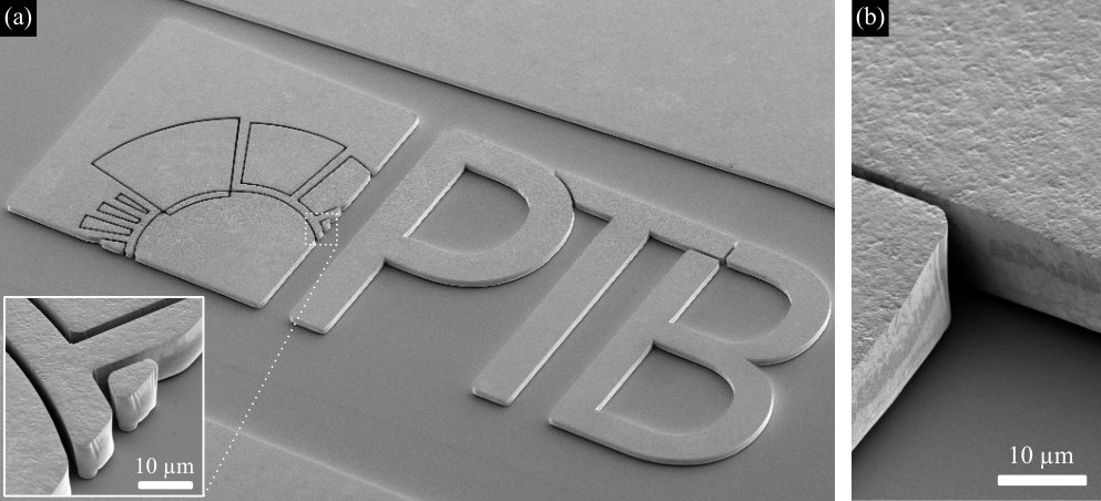 Figure 1
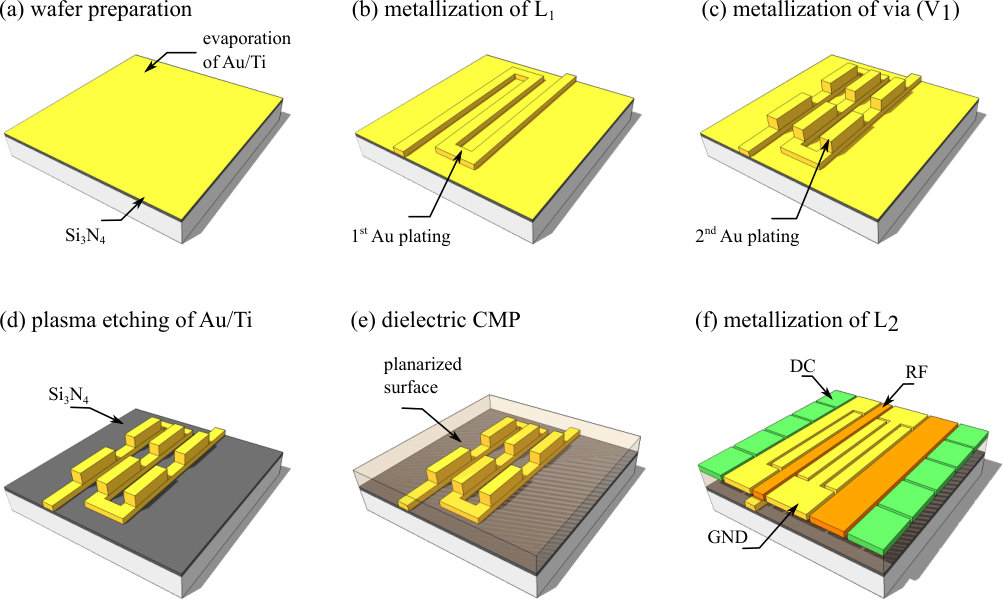 Figure 2
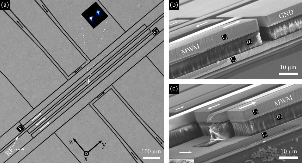 Figure 3
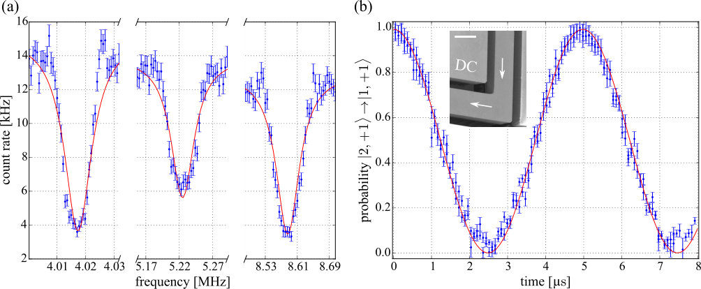 Figure 4
Peer Reviews
No public reviews on file for this paper yet. If you reviewed it on a platform where reviews are public (OpenReview, ICLR, NeurIPS, ICML), you can paste yours below so the community can read it here.
Videos
No videos yet. Explain this paper in a talk, walkthrough, or lecture? Add one.
Multilayer ion trap technology for scalable quantum computing and quantum simulation
A. Bautista-Salvador1,2,3, G. Zarantonello1,2, H. Hahn1,2, A. Preciado-Grijalva1, J. Morgner1,2, M. Wahnschaffe1,2,3, C. Ospelkaus1,2,3
1 Physikalisch-Technische Bundesanstalt, Bundesallee 100, 38116 Braunschweig, Germany
2 Institute of Quantum Optics, Leibniz Universität Hannover, Welfengarten 1, 30167 Hannover, Germany
3 Laboratory for Nano- and Quantum Engineering, Leibniz Universität Hannover, Schneiderberg 39, 30167 Hannover, Germany
Abstract
We present a novel ion trap fabrication method enabling the realization of multilayer ion traps scalable to an in principle arbitrary number of metal-dielectric levels. We benchmark our method by fabricating a multilayer ion trap with integrated three-dimensional microwave circuitry. We demonstrate ion trapping and microwave control of the hyperfine states of a laser cooled 9Be+ ion held at a distance of above the trap surface. This method can be used to implement large-scale ion trap arrays for scalable quantum information processing and quantum simulation.
1 Introduction
Trapped ions are not only one of the most promising platforms for the practical implementation of quantum computing and quantum simulations, but also sensitive systems for measuring very small magnetic and electric fields. Typically, they are held in Paul or Penning traps at high vacuum, laser cooled close to absolute zero temperature, and their internal states coupled to their motion can be manipulated with high fidelity by either laser fields [1, 2] or microwave radiation [3, 4]. However, scaling these elementary demonstrations to larger systems remains a formidable technological challenge [5].
Surface-electrode ion traps [6] represent a strong candidate for the realization of a quantum charge-coupled device (QCCD) [7, 8] for scaling quantum logic operations. Such an ion trap array could feature dedicated zones for storing, manipulation and read-out, thus promising a modular hardware for quantum computation and quantum simulation [9]. Conventionally, in surface-electrode ion traps all electrodes are built in a single plane by standard microfabrication techniques [10]. First integration of key scalable elements into a single layer chip such as micro-optical components [11], nanophotonic waveguide devices [12] or microwave conductors [13] have been demonstrated. However, interconnecting separated components built in this system imposes new challenges on trap design where signal lines have to be routed around other elements. Therefore, the realization of a highly integrated large-scale ion trap device requires a more flexible approach where signal routings can be distributed on vertically well-separated levels of interconnects.
Demonstrations of multilayer processes in ion traps so far are based on techniques borrowed from MicroElectroMechanical Systems (MEMS) [14, 15] or CMOS [16, 17]; however the resulting trap structures are limited to thin interconnect levels. Moreover, there is a need of a nearly material-independent processing capable of including most dielectric substrates and thick metallization. Any fabrication process will have to comply with the specific requirements of an ion trap, such as a material mix which features extremely low material outgassing and needs to be compatible with ultra-high vacuum (UHV) operation, low dielectric losses and non-magnetic metal surfaces. Often one is concerned about shielding the ion(s) from patch potentials due to exposed dielectrics. Specially, for the top-level the electrode interspacings should have at least a width equal to its height [18], or in other words electrode gaps of an aspect ratio higher than 1:1.
Here we present a robust fabrication method, scalable to an in principle arbitrary number of planarized thick metal-dielectric layers, enabling the realization of scalable ion trap devices. The method complies with the stringent requirements of a scalable ion trapping array, allowing the fabrication of complex trap designs using relatively forgiving fabrication techniques on nearly any type of substrate. To demonstrate the approach, we fabricate and operate a multilayer ion trap chip with three-dimensional (3-D) microwave circuitry towards the realization of high fidelity muli-qubit gates [13, 19].
2 Fabrication Methods
Methods for building surface-electrode ion traps [6] or atom chips [20, 21] are typically based on standard semiconductor processing. For the simplest case, in which all metal electrodes are aligned in a single plane, a generic fabrication workflow consists of a three-step processing: wafer patterning, electrode formation and electric insulation. Depending on the requirements one will choose between different materials and processing methods at hand. In what follows we will describe our own fabrication methods to build single layer and multilayer microfabricated ion traps.
2.1 Single Level Processing (SLP) Method
For the Single Level Processing (SLP) method all steps are carried out on 3-inch-diameter wafers in a fabrication line located at Physikalisch-Technische Bundesanstalt (PTB), Braunschweig. We have fabricated similar structures to the ones presented in Fig. 1 on AlN, sapphire, organic polymers and high resistivity (HiR) float zone (FZ) Si wafers, demonstrating the compatibility of the method with a wide range of substrates suitable for ion trap technology.
The first step during wafer preparation involves the deposition of a Ti adhesion layer ( thin) and an Au seed layer ( thin) on top of the substrate by resistive evaporation. The first film acts as an adhesion promoter between the substrate and the Au seed layer, and the second film serves as a starting conductive layer for a later electrodeposition step.
Second, to define the trap geometry, a 25--thick positive or 16--thick negative resist is spin coated on top of the Au seed layer and the wafer is exposed to UV light by contact lithography. A subsequent development of the exposed resist results in open areas on the substrate which are filled to a desired thickness by electrodeposition of Au in a sulphite-based bath.
Finally, after gold electroplating the resist mask is removed chemically and the wafer is cleaned under oxygen-based plasma etching. Additionally, the wafer is exposed to a fluorine-based plasma to further remove possible resist debris. Immediately afterwards the seed Au layer is removed via Ar etching and the Ti layer removed by a fluorine-based plasma etching.
This method allows the fabrication of gold structures with high aspect ratios as exemplified in Fig 1. Gold structures with a width as narrow as and gap separation as narrow as are shown in Fig. 1(a). Another example is depicted in Fig. 1(b) consisting of a pair of gold electrodes separated by a gap with an aspect ratio of 14:1. One additional advantage of the method is that after dry etching of the Au/Ti bilayer the resulting trap surfaces have a superior finishing quality compared to the commonly used wet etching.
2.2 Multilevel Processing (MLP) Method
In this section a Multilevel Processing (MLP) method is presented, which combines techniques borrowed from MicroElectroMechanical Systems (MEMS) and Integrated Circuits (IC) processing. The method is also compatible with other common substrates used for ion trap technology such as silicon, sapphire, borosilicate glass and quartz.
To demonstrate the simplicity and robustness of our method we have fabricated an ion trap with integrated (3-D) three-dimensional microwave circuitry. It comprises a lower interconnect level and an upper electrode level . An additional vertical interconnect access , called via, allows microwave signals to be transmitted between levels. A more detailed description of the microwave and quantum logic aspects of the trap design and the corresponding characterization will be covered elsewhere [22].
The method presented here mainly consists of six processing steps: (a) wafer preparation, (b) metallization of lower level , (c) metallization of via , (d) removal of seed layer, (e) deposition and planarization of dielectric layer and (f) metallization of upper level . A schematics of the fabrication flow is given in Fig. 2.
The supporting material is a 3-inch silicon wafer with high resistivity (1\text{\times}{10}^{4}\text{,}\mathrm{\SIUnitSymbolOhm}\text{,}\mathrm{cm}$$). On top of it and as shown in Fig. 2(a), a 2--thick film of Si3N4 is deposited by physical enhanced chemical vapor deposition (PECVD). This dielectric film may improve trap operation by avoiding detrimental diffussion of Au into silicon and increasing the flashover voltage as demonstrated in Ref. [23]. Thereafter, a 10--thin layer of Ti and a 50--thin layer of Au are thermally evaporated on top of Si3N4.
To build the lower level on top of Si3N4/Si, a negative resist is spin coated and patterned via UV lithography. Once the negative resist is developed to form a resist mold, gold electrodes are grown by electroplating as depicted in Fig. 2(b). After electroplating is completed, the resist mask is stripped and the wafer cleaned under plasma etching.
For the metallization of the via we repeat the photolithography and electroplating steps presented in (b) but this time on top of by using a thick (12\text{,}\mathrm{\SIUnitSymbolMicro m}$$) developed negative resist as a plating mold. Electroplated vias on top of L1 are depicted in Fig. 2(c) after stripping the negative resist mask and plasma cleaning of the wafer.
To remove the Au seed layer and the Ti adhesion layer we use the last dry etching step from the SLP method. This step allows a controllable etch of Au and Ti of and respectively, resulting in a minimal change of the surface quality on top of both and surfaces. The electrically isolated elements on and are schematically illustrated in Fig. 2(d).
A dielectric layer is then spin coated on top of and and thermally cured (Fig. 2(e)). After thermal curing, excess material is present on top of the underlaying structures in and . The imprinted dielectric topography is globally planarized through a chemical-mechanical polishing (CMP) step, which is stopped at the top of or close to it. To assure electrical contact between and the subsequent level a local etch-back process is performed.
To define the top metal layer the SLP method is again employed but this time on top of the planarized polymer surface (Fig. 2(f)). Once the plating has been completed and the resist mold removed, the remaining polymer film between gaps underneath L2 is etched down to the Si3N4 layer by a fluorine-based plasma to hide possible patch potentials built on the exposed insulator.
3 Fabrication outcome and trap operation
Here we briefly present the design and characterization of a trap with 3-D microwave conductors integrated into a microfabricated ion trap using the MLP method. The microwave circuitry is embedded to implement quantum logic operations using near-field microwaves [24, 13, 25, 26]. The specific design is discussed elsewhere in detail [hahn_multilayer_2018] and here only described as one of many scenarios that benefits from the multilayer technology.
In the upper level (L2) the trap includes two RF electrodes and ten DC electrodes to confine the ions to a local minimum (), see Fig. 3(a). A microwave signal (white arrows) of frequency can be applied on a 3-D microwave meander (MWM) conductor between two contact points labeled as “F” and “G”, thus generating an oscillating magnetic near-field gradient in the radial plane with a local minimum at . The three apparent independent microwave conductors indicated by the white arrows are indeed part of a single 3-D microwave meander connected to L1 by vias and routed over L1 as inidicated in Fig. 3. A central part of a diced trap chip (5\text{\,}\mathrm{mm}$\times$5\text{\,}\mathrm{mm}) fabricated using the MLP method is presented in Fig. 3(a). There are also two additional microwave conductors (MWC) surrounding the central DC electrodes, in which an oscillating current (black arrows) can be applied to produce an oscillating field.
A cleaved chip revealing a cross-section view of the metal-dielectric stack around position “F” position “G” is shown in Fig. 3(b) and Fig. 3(c)), respectively. The ion trap (RF and DC electrodes) as well as the uppermost part of the MWM conductor are entirely located in L2, whereas the microwave signals and the ground plane are routed between L1 and L2 through vias in V1 (not visible in the micrograph but behind D1 in Fig. 3(b) and (c)).
Removing both Au and Ti films by means of dry etching has improved the trap surface quality. For a similar chip as the one here presented an rms roughness 8.3(5)\text{,}\mathrm{nm}25\text{,}\mathrm{\SIUnitSymbolMicro m}25\text{,}\mathrm{\SIUnitSymbolMicro m}$$. This represents a two-order of magnitude improvement when compared to a wet etching process using aqua regia [27]. These nearly mirror-like surfaces are relevant since there is a reduction of stray light scattered in the direction perpendicular to the trap surface during resonance fluorescence imaging for ion state detection. Also an ion trap with minimal surface roughness might be less prone to anomalous motional heating at cryogenic temperatures [28].
The diced trap chip is glued onto a copper block and wirebonded to a custom printed circuit board for filtering and signal routing. The whole assembly is installed in a vacuum system at a pressure better than and connected to an in-vacuum coaxial resonator similar to the one used in Ref. [29]. For ion loading we employ a laser ablation scheme [27] and subsequent two-photon ionization using light [30]. Single 9Be+ ions are loaded at above the upper surface of around the position “X” (see Fig. 3(a)).
We supply to the trap an RF drive frequency of 176.5\text{,}\mathrm{MHz} with amplitude $\text{V}_{RF}=$100\text{\,}\mathrm{V} and DC voltages ranging within 25\text{,}\mathrm{V}$$. To determine the trap frequencies we apply an oscillating tickle voltage to one of the DC electrodes and scan the frequency [31]. Once the tickle drive is resonant with a secular frequency, the motion of the ion is excited and the ion fluorescence drops (Fig. 4(a)). We measure secular trap frequencies of , where the high-frequency (HF) and low-frequency (LF) radial modes form an angle of relative to the -axis and -axis, respectively.
Finally we employ the integrated microwave conductors to manipulate the internal state of the ion. Fig. 4(b) shows Rabi oscillations on the qubit transition [27] of the electronic ground state of a single 9Be+ ion at an external magnetic field of 22.3\text{,}\mathrm{mT} when applying a microwave current of frequency $\omega_{0}\simeq$1082.55\text{\,}\mathrm{MHz} to one of the MWC conductors. Here, is referring to the total angular momentum and the quantum number of its projection on . The state readout is carried out via ion fluorescence detection on the closed-cycling transition , combined with suitable microwave transfer pulses [27].
4 Conclusion and Outlook
We have presented a novel multilayer method for fabricating scalable surface-electrode ion traps. The flexibility and robustness of the method allows to benchmark the integration of 3-D microwave circuitry into a multilayer ion trap. Furthermore, we have demonstrated successful trapping of 9Be+ and basic qubit manipulation by applying microwave oscillating currents on one of the conductors.
The MLP method presented here can in principle be extended to a nearly arbitrary number of layers to comply with the stringent needs of scaling surface-electrode ion traps. Moreover, the method permits the integration of three-dimensional and planarized features with high aspect ratio. This technique opens new routes towards the realization of more complex and powerful ion trap devices.
In contrast to a typical CMOS situation where the “device” is fabricated on top of the substrate, with interconnect layers on top of the device, in our case the “device” is the top electrode layer which is controlling the ion(s), whereas the layers closer to the substrate are used as interconnects. In the future, these lower interconnects may be combined with through-wafer vias to achieve contacting of the ion trap chip from the backside, eliminating the need of wirebonds and likely obstruction of laser beams. Through-wafer slots for back-side ion loading can also be produced in the same way. These same techniques could be applied to realize so-called analog quantum simulators in ion trap arrays [32, 33, 34], possibly with integrated control [35]. Moreover, such an approach may enable the embedding of complex integrated components such as trench capacitors [36, 37], low-loss integrated waveguides [38]; or the realization of more elaborate devices including reliable ion-transport junctions [39, 40], increased optical access [17] or manipulation of scalable arrays of two-dimensional trapped ion systems [33, 34].
The MLP method can also be used to extend multilayer “atom chips” [21, 41, 42] or to fabricate scalable hybrid atom-ion traps [43, 44] for quantum many-body physics experiments and quantum sensing with neutral atoms. In this context the thick metal conductors can support substantial currents required for magnetic trapping and the planarization together with the demonstrated minimized surface roughness allows the implementation of mirror-like surfaces and transfer coatings for integrated magneto-optical traps.
Acknowledgements
We acknowledge support by the PTB cleanroom facility team, in particular T. Weimann and P. Hinze. We also acknowledge support by the LNQE cleanroom staff in particular O. Kerker. We acknowledge funding from PTB, QUEST, LUH, NTH (project number 2.2.11) and DFG through CRC 1227 DQ-mat, project A01.
References
- [1]
Gaebler J, Tan T, Lin Y, Wan Y, Bowler R, Keith A, Glancy S, Coakley K, Knill E, Leibfried D and Wineland D 2016 Physical Review Letters 117 060505 URL http://link.aps.org/doi/10.1103/PhysRevLett.117.060505
- [2]
Ballance C, Harty T, Linke N, Sepiol M and Lucas D 2016 Physical Review Letters 117 060504 URL http://link.aps.org/doi/10.1103/PhysRevLett.117.060504
- [3]
Harty T, Sepiol M, Allcock D, Ballance C, Tarlton J and Lucas D 2016 Physical Review Letters 117 140501 URL http://link.aps.org/doi/10.1103/PhysRevLett.117.140501
- [4]
Weidt S, Randall J, Webster S, Lake K, Webb A, Cohen I, Navickas T, Lekitsch B, Retzker A and Hensinger W 2016 Physical Review Letters 117 ISSN 0031-9007, 1079-7114 URL https://link.aps.org/doi/10.1103/PhysRevLett.117.220501
- [5]
Monroe C and Kim J 2013 Science 339 1164–1169 ISSN 0036-8075, 1095-9203 URL http://science.sciencemag.org/content/339/6124/1164
- [6]
Seidelin S, Chiaverini J, Reichle R, Bollinger J J, Leibfried D, Britton J, Wesenberg J H, Blakestad R B, Epstein R J, Hume D B, Itano W M, Jost J D, Langer C, Ozeri R, Shiga N and Wineland D J 2006 Physical Review Letters 96 253003 URL http://link.aps.org/doi/10.1103/PhysRevLett.96.253003
- [7]
Wineland D J, Monroe C R, Itano W M, Leibfried D, King B E and Meekhof D M 1998 J. Res. NIST 103 259–328 URL http://http://nvl.nist.gov/pub/nistpubs/jres/103/3/j33win.pdf
- [8]
Kielpinski D, Monroe C and Wineland D J 2002 Nature 417 709–711 ISSN 0028-0836 URL http://dx.doi.org/10.1038/nature00784
- [9]
Lekitsch B, Weidt S, Fowler A G, Mølmer K, Devitt S J, Wunderlich C and Hensinger W K 2017 Science Advances 3 e1601540 ISSN 2375-2548 URL http://advances.sciencemag.org/content/3/2/e1601540
- [10]
Hughes M D, Lekitsch B, Broersma J A and Hensinger W K 2011 Contemporary Physics 1–25 ISSN 0010-7514, 1366-5812 URL http://www.tandfonline.com/doi/abs/10.1080/00107514.2011.601918
- [11]
Merrill J T, Volin C, Landgren D, Amini J M, Wright K, Doret S C, C-S Pai, Hayden H, Killian T, Faircloth D, Brown K R, Harter A W and Slusher R E 2011 New Journal of Physics 13 103005 ISSN 1367-2630 URL http://stacks.iop.org/1367-2630/13/i=10/a=103005
- [12]
Mehta K K, Bruzewicz C D, McConnell R, Ram R J, Sage J M and Chiaverini J 2016 Nature Nanotechnology 11 1066–1070 ISSN 1748-3387 URL http://www.nature.com/nnano/journal/v11/n12/full/nnano.2016.139.html
- [13]
Ospelkaus C, Warring U, Colombe Y, Brown K R, Amini J M, Leibfried D and Wineland D J 2011 Nature 476 181–184 ISSN 0028-0836 URL http://dx.doi.org/10.1038/nature10290
- [14]
Cho D I D, Hong S, Lee M and Kim T 2015 Micro and Nano Systems Letters 3 1 ISSN 2213-9621 URL http://mnsl-journal.springeropen.com/articles/10.1186/s40486-015-0013-3
- [15]
Hong S, Lee M, Cheon H, Kim T and Cho D i D 2016 Sensors 16 616 URL http://www.mdpi.com/1424-8220/16/5/616
- [16]
Stick D, Fortier K M, Haltli R, Highstrete C, Moehring D L, Tigges C and Blain M G 2010 1008.0990 URL http://arxiv.org/abs/1008.0990
- [17]
Maunz P L W 2016 High Optical Access Trap 2.0. Tech. Rep. SAND-2016-0796R Sandia National Lab. (SNL-NM), Albuquerque, NM (United States) URL https://www.osti.gov/biblio/1237003-high-optical-access-trap
- [18]
Schmied R 2010 New Journal of Physics 12 023038 ISSN 1367-2630 URL http://iopscience.iop.org/1367-2630/12/2/023038
- [19]
Timoney N, Baumgart I, Johanning M, Varon A F, Plenio M B, Retzker A and Wunderlich C 2011 Nature 476 185–188 ISSN 0028-0836 URL http://dx.doi.org/10.1038/nature10319
- [20]
Treutlein P 2008 Coherent manipulation of ultracold atoms on atom chips Ph.D. thesis Ludwig-Maximilians-Universität München
- [21]
Fortágh J and Zimmermann C 2007 Reviews of Modern Physics 79 235 URL http://link.aps.org/doi/10.1103/RevModPhys.79.235
- [22]
Hahn H, Zarantonello G, Bautista-Salvador A, Kohnen M, Wahnschaffe M, Ospelkaus C and Schoebel J in preparation
- [23]
Sterling R C, Hughes M D, Mellor C J and Hensinger W K 2013 Applied Physics Letters URL http://aip.scitation.org/doi/10.1063/1.4824012
- [24]
Ospelkaus C, Langer C E, Amini J M, Brown K R, Leibfried D and Wineland D J 2008 Physical Review Letters 101 090502 URL http://link.aps.org/doi/10.1103/PhysRevLett.101.090502
- [25]
Warring U, Ospelkaus C, Colombe Y, Brown K R, Amini J M, Carsjens M, Leibfried D and Wineland D J 2013 Physical Review A 87 013437 URL http://link.aps.org/doi/10.1103/PhysRevA.87.013437
- [26]
Carsjens M, Kohnen M, Dubielzig T and Ospelkaus C 2014 Applied Physics B 114 243–250 ISSN 0946-2171, 1432-0649 URL http://link.springer.com/article/10.1007/s00340-013-5689-6
- [27]
Wahnschaffe M, Hahn H, Zarantonello G, Dubielzig T, Grondkowski S, Bautista-Salvador A, Kohnen M and Ospelkaus C 2017 Applied Physics Letters 110 034103 ISSN 0003-6951 URL http://aip.scitation.org/doi/full/10.1063/1.4974736
- [28]
Lin K Y, Low G H and Chuang I L 2016 Physical Review A 94 013418 URL https://link.aps.org/doi/10.1103/PhysRevA.94.013418
- [29]
Jefferts S R, Monroe C, Bell E W and Wineland D J 1995 Physical Review A 51 3112 URL http://link.aps.org/doi/10.1103/PhysRevA.51.3112
- [30]
Leibrandt D R, Clark R J, Labaziewicz J, Antohi P, Bakr W, Brown K R and Chuang I L 2007 Physical Review A 76 055403 URL http://link.aps.org/doi/10.1103/PhysRevA.76.055403
- [31]
Home J P, Hanneke D, Jost J D, Leibfried D and Wineland D J 2011 New Journal of Physics 13 073026 ISSN 1367-2630 URL http://stacks.iop.org/1367-2630/13/i=7/a=073026
- [32]
Porras D and Cirac J I 2004 Physical Review Letters 92 207901 URL http://link.aps.org/doi/10.1103/PhysRevLett.92.207901
- [33]
Mielenz M, Kalis H, Wittemer M, Hakelberg F, Warring U, Schmied R, Blain M, Maunz P, Moehring D L, Leibfried D and Schaetz T 2016 Nature Communications 7 ncomms11839 ISSN 2041-1723 URL https://www.nature.com/articles/ncomms11839
- [34]
Bruzewicz C D, McConnell R, Chiaverini J and Sage J M 2016 Nature Communications 7 ISSN 2041-1723 URL http://www.nature.com/articles/ncomms13005
- [35]
Chiaverini J and Lybarger W E 2008 Physical Review A 77 022324 URL http://link.aps.org/doi/10.1103/PhysRevA.77.022324
- [36]
Allcock D T C, Harty T P, Janacek H A, Linke N M, Ballance C J, Steane A M, Lucas D M, Jarecki R L, Habermehl S D, Blain M G, Stick D and Moehring D L 2012 Applied Physics B 107 913–919 ISSN 0946-2171, 1432-0649 URL http://link.springer.com/article/10.1007/s00340-011-4788-5
- [37]
Guise N D, Fallek S D, Stevens K E, Brown K R, Volin C, Harter A W, Amini J M, Higashi R E, Lu S T, Chanhvongsak H M, Nguyen T A, Marcus M S, Ohnstein T R and Youngner D W 2015 Journal of Applied Physics 117 174901 ISSN 0021-8979 URL https://aip.scitation.org/doi/10.1063/1.4917385
- [38]
West G N, Loh W, Kharas D, Sorace-Agaskar C, Mehta K K, Sage J, Chiaverini J and Ram R J 2018 arXiv:1808.00429 [physics] ArXiv: 1808.00429 URL http://arxiv.org/abs/1808.00429
- [39]
Moehring D L, Highstrete C, Stick D, Fortier K M, Haltli R, Tigges C and Blain M G 2011 New Journal of Physics 13 075018 ISSN 1367-2630 URL http://stacks.iop.org/1367-2630/13/i=7/a=075018
- [40]
Wright K, Amini J M, Faircloth D L, Volin C, Doret S C, Hayden H, C-S Pai, Landgren D W, Denison D, Killian T, Slusher R E and Harter A W 2013 New Journal of Physics 15 033004 ISSN 1367-2630 URL http://stacks.iop.org/1367-2630/15/i=3/a=033004
- [41]
Trinker M, Groth S, Haslinger S, Manz S, Betz T, Schneider S, Bar-Joseph I, Schumm T and Schmiedmayer J 2008 Applied Physics Letters 92 254102 ISSN 0003-6951 URL http://aip.scitation.org/doi/full/10.1063/1.2945893
- [42]
Bohi P, Riedel M F, Hoffrogge J, Reichel J, Hansch T W and Treutlein P 2009 Nature Physics 5 592–597 ISSN 1745-2473 URL http://dx.doi.org/10.1038/nphys1329
- [43]
Härter A and Denschlag J H 2014 Contemporary Physics 55 33–45 ISSN 0010-7514 URL https://doi.org/10.1080/00107514.2013.854618
- [44]
Bahrami A, Müller M, Drechsler M, Joger J, Gerritsma R and Schmidt-Kaler F 2018 arXiv:1811.07670 [physics, physics:quant-ph] ArXiv: 1811.07670 URL http://arxiv.org/abs/1811.07670
The reference list from the paper itself. Each links out to its DOI / PubMed record.
- 1[1] Gaebler J, Tan T, Lin Y, Wan Y, Bowler R, Keith A, Glancy S, Coakley K, Knill E, Leibfried D and Wineland D 2016 Physical Review Letters 117 060505 URL http://link.aps.org/doi/10.1103/Phys Rev Lett.117.060505
- 2[2] Ballance C, Harty T, Linke N, Sepiol M and Lucas D 2016 Physical Review Letters 117 060504 URL http://link.aps.org/doi/10.1103/Phys Rev Lett.117.060504
- 3[3] Harty T, Sepiol M, Allcock D, Ballance C, Tarlton J and Lucas D 2016 Physical Review Letters 117 140501 URL http://link.aps.org/doi/10.1103/Phys Rev Lett.117.140501
- 4[4] Weidt S, Randall J, Webster S, Lake K, Webb A, Cohen I, Navickas T, Lekitsch B, Retzker A and Hensinger W 2016 Physical Review Letters 117 ISSN 0031-9007, 1079-7114 URL https://link.aps.org/doi/10.1103/Phys Rev Lett.117.220501
- 5[5] Monroe C and Kim J 2013 Science 339 1164–1169 ISSN 0036-8075, 1095-9203 URL http://science.sciencemag.org/content/339/6124/1164
- 6[6] Seidelin S, Chiaverini J, Reichle R, Bollinger J J, Leibfried D, Britton J, Wesenberg J H, Blakestad R B, Epstein R J, Hume D B, Itano W M, Jost J D, Langer C, Ozeri R, Shiga N and Wineland D J 2006 Physical Review Letters 96 253003 URL http://link.aps.org/doi/10.1103/Phys Rev Lett.96.253003
- 7[7] Wineland D J, Monroe C R, Itano W M, Leibfried D, King B E and Meekhof D M 1998 J. Res. NIST 103 259–328 URL http://http://nvl.nist.gov/pub/nistpubs/jres/103/3/j 33win.pdf
- 8[8] Kielpinski D, Monroe C and Wineland D J 2002 Nature 417 709–711 ISSN 0028-0836 URL http://dx.doi.org/10.1038/nature 00784 · doi ↗