Nonvolatile Solid-State Charged-Polymer Gating of Topological Insulators into the Topological Insulating Regime
R. M. Ireland, Liang Wu, M. Salehi, S. Oh, N. P. Armitage, and H. E., Katz

TL;DR
This paper introduces a novel non-volatile electrostatic gating method using charged polymers to effectively tune the carrier density of topological insulator Bi2Se3, achieving stable Fermi level control and enhanced electron mobility.
Contribution
It presents the first use of charged polymer gating to modulate the charge density in topological insulators without continuous gate connection or chemical modification.
Findings
Fermi level shifted close to the Dirac point
Surface chemical potential lowered into the bulk band gap
Electron mobility enhanced to ~1600 cm^2/Vs at 5K
Abstract
We demonstrate the ability to reduce the carrier concentration of thin films of the topological insulator (TI) Bi2Se3 by utilizing a novel approach, namely non-volatile electrostatic gating via corona charging of electret polymers. Sufficient electric field can be imparted to a polymer-TI bilayer to result in significant electron density depletion, even without the continuous connection of a gate electrode or the chemical modification of the TI. We show that the Fermi level of Bi2Se3 is shifted towards the Dirac point with this method. Using THz spectroscopy, we find that the surface chemical potential is lowered into the bulk band gap (~ 50 meV above the Dirac point and 170 meV below the conduction band minimum) and it is stabilized in the intrinsic regime while enhancing electron mobility. This represents the first use of a charged polymer gate for modulating TI charge density. The…
Click any figure to enlarge with its caption.
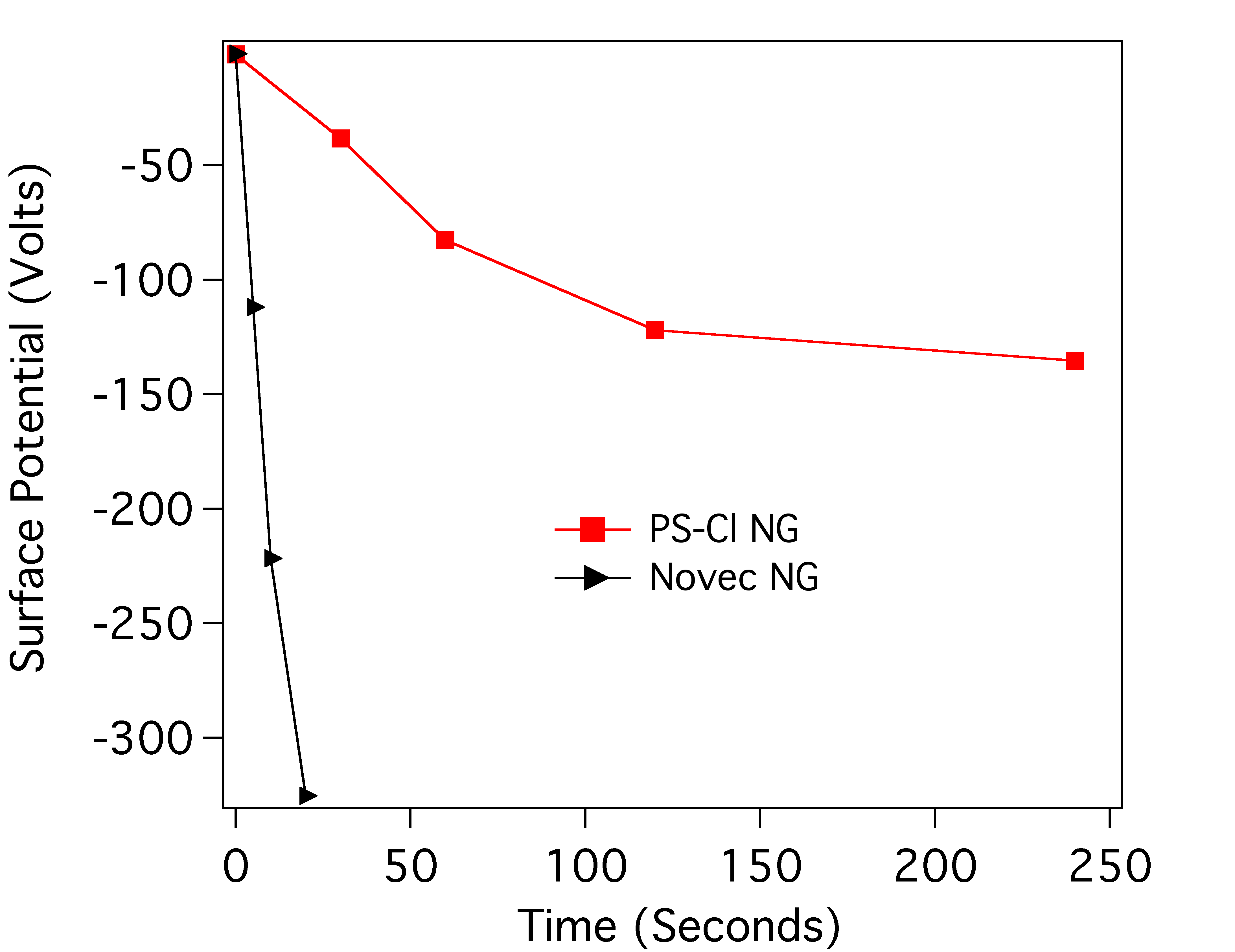 Figure 1
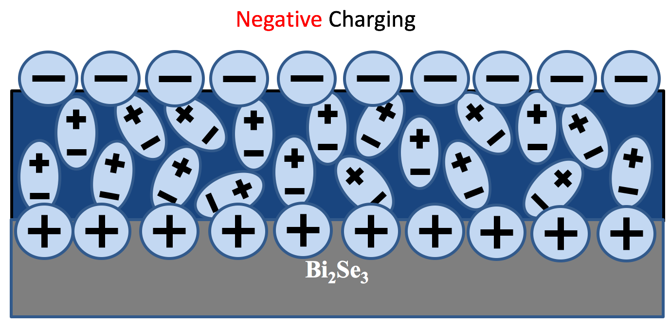 Figure 2
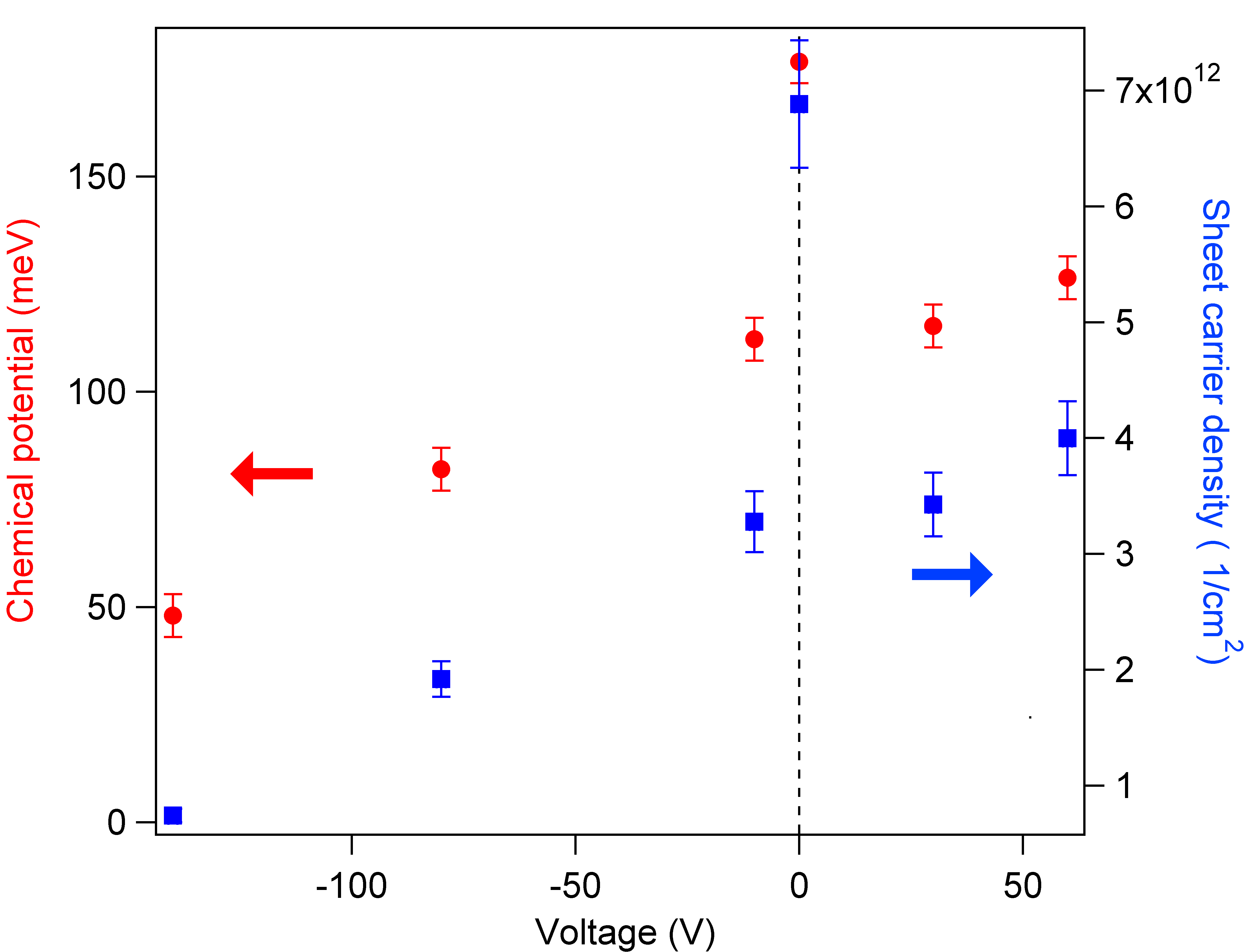 Figure 3
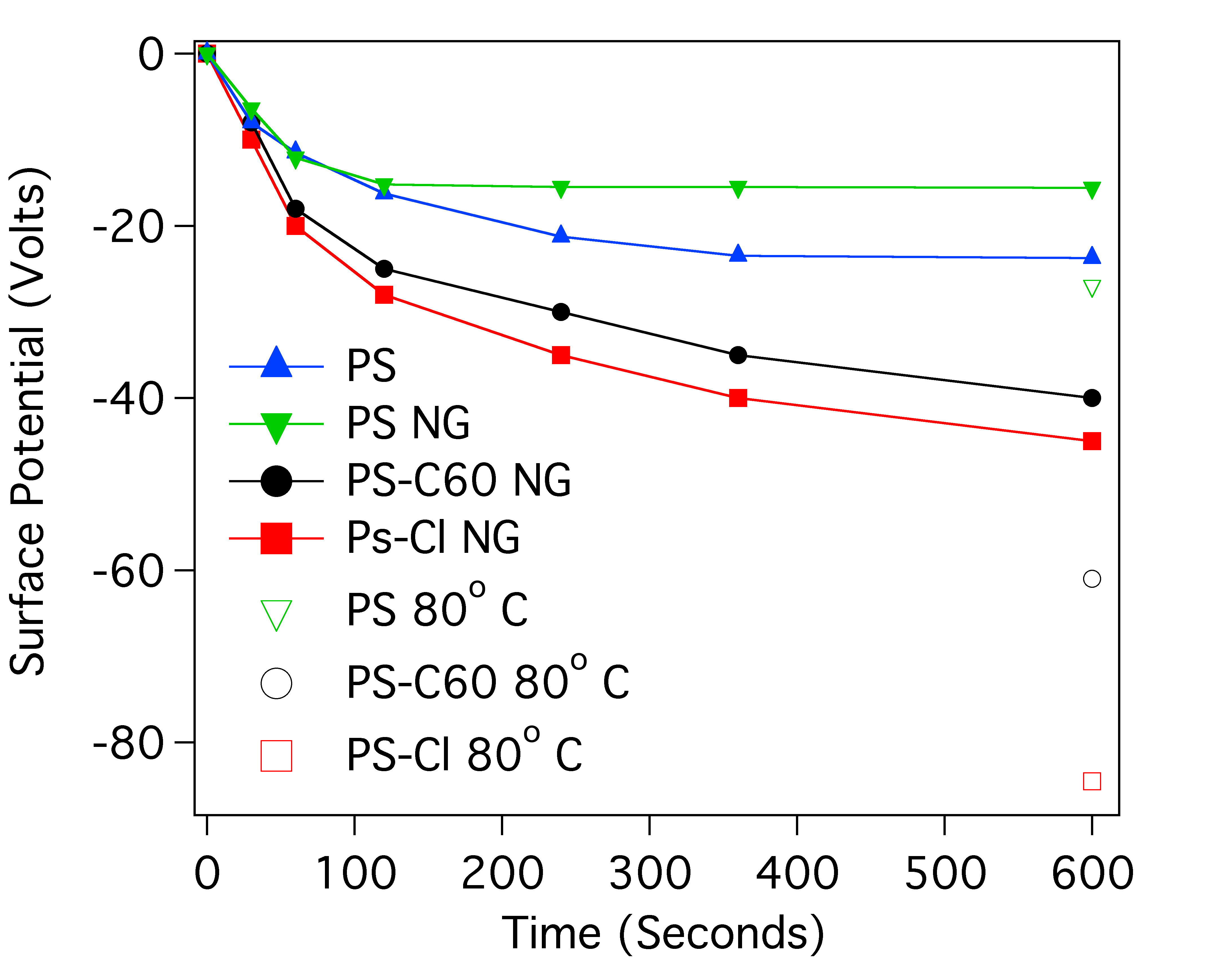 Figure 4
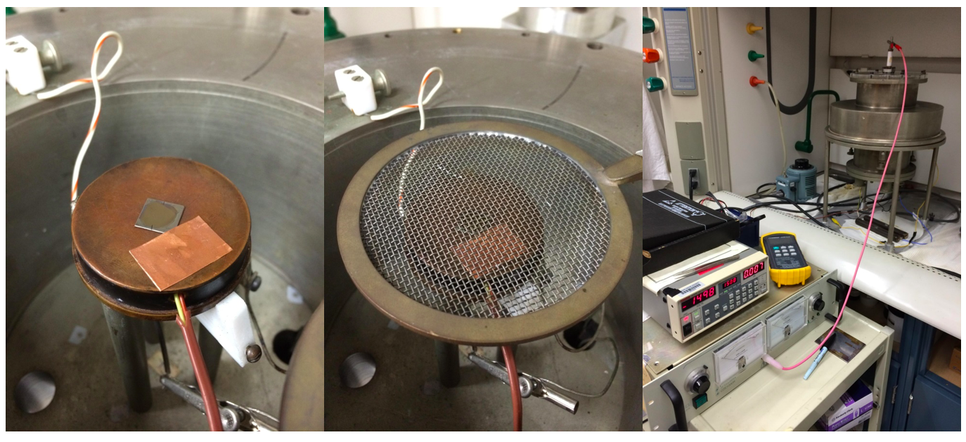 Figure 5
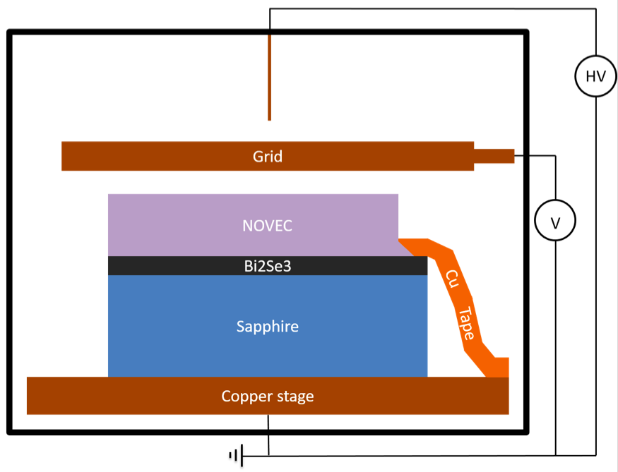 Figure 6
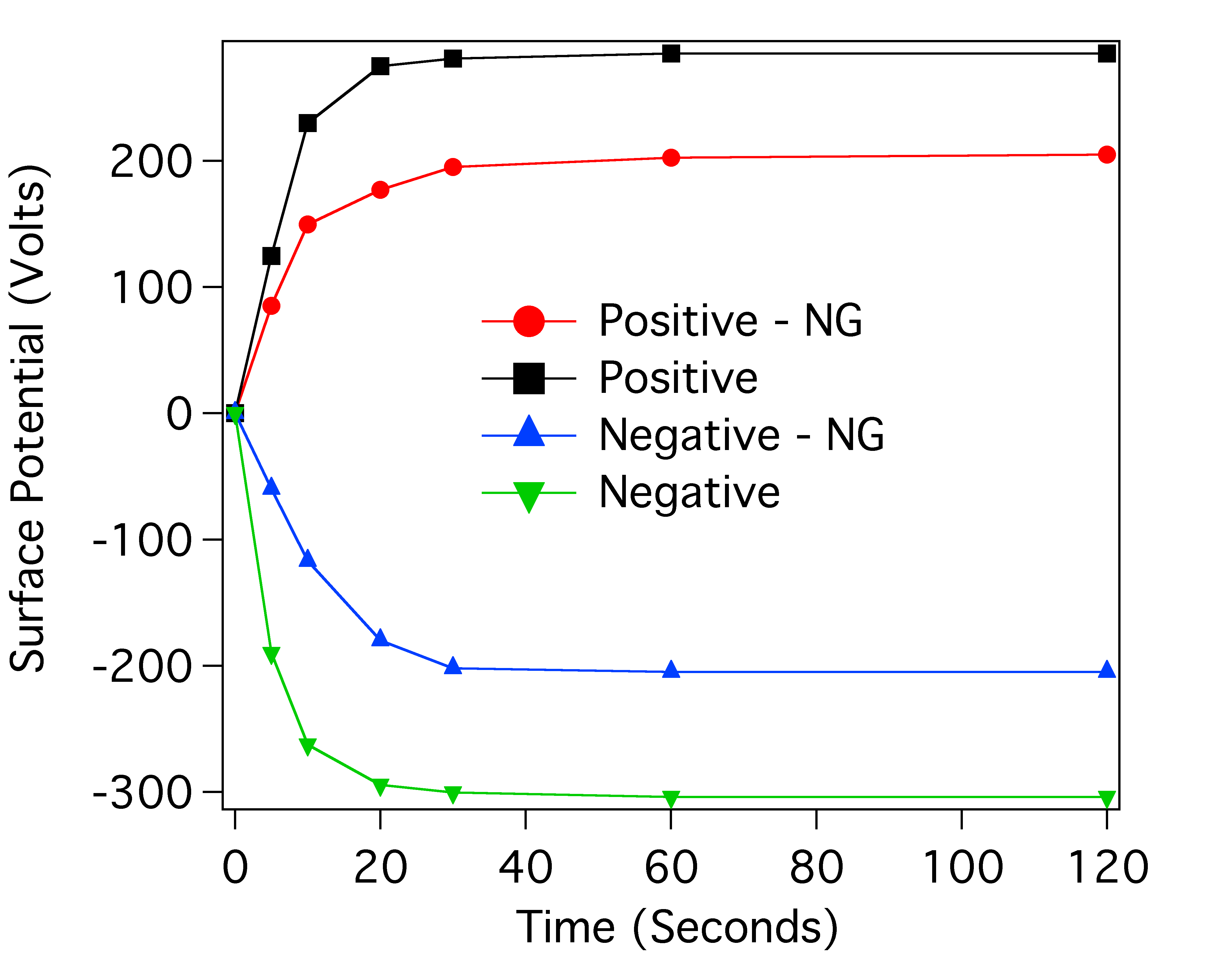 Figure 7
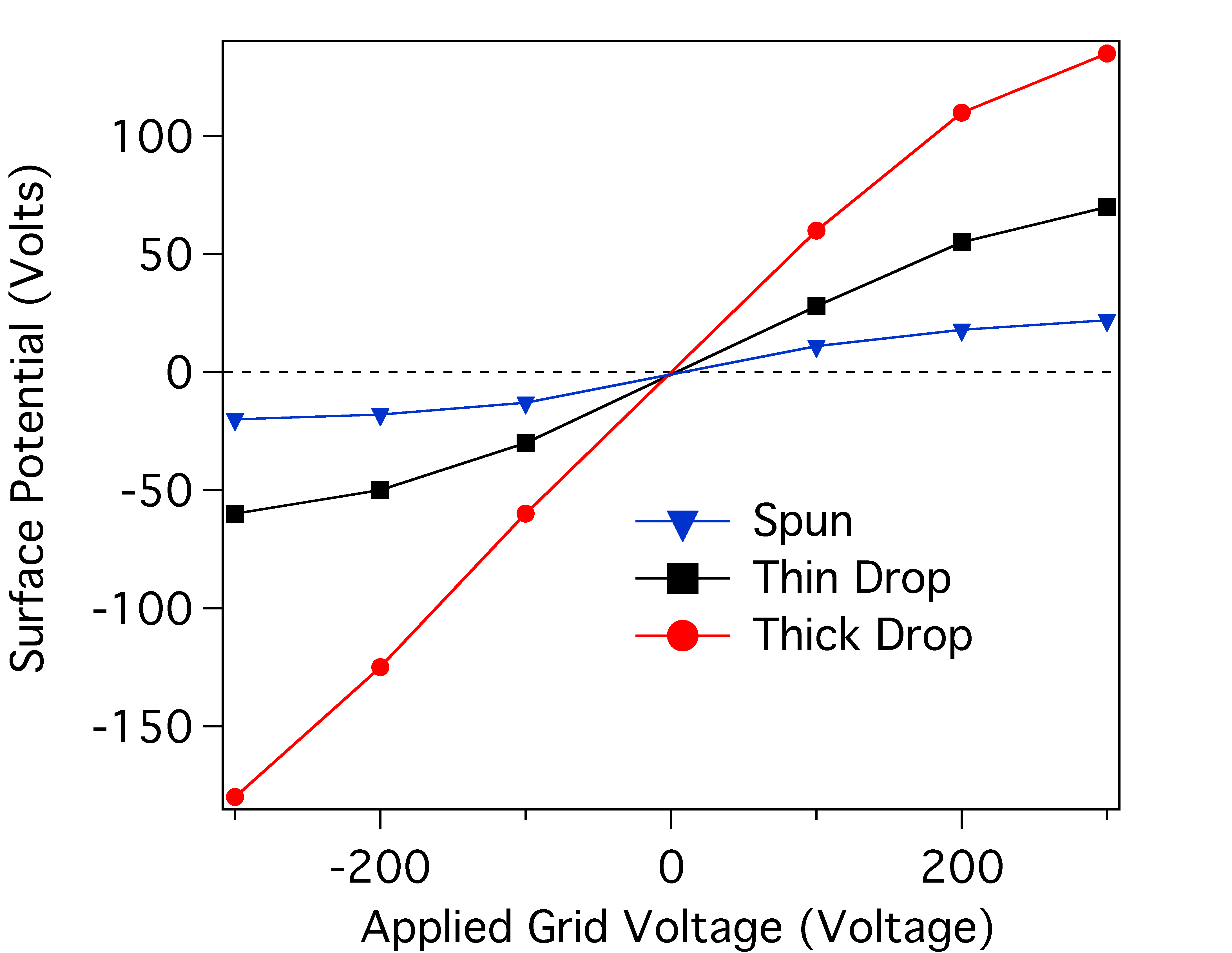 Figure 8
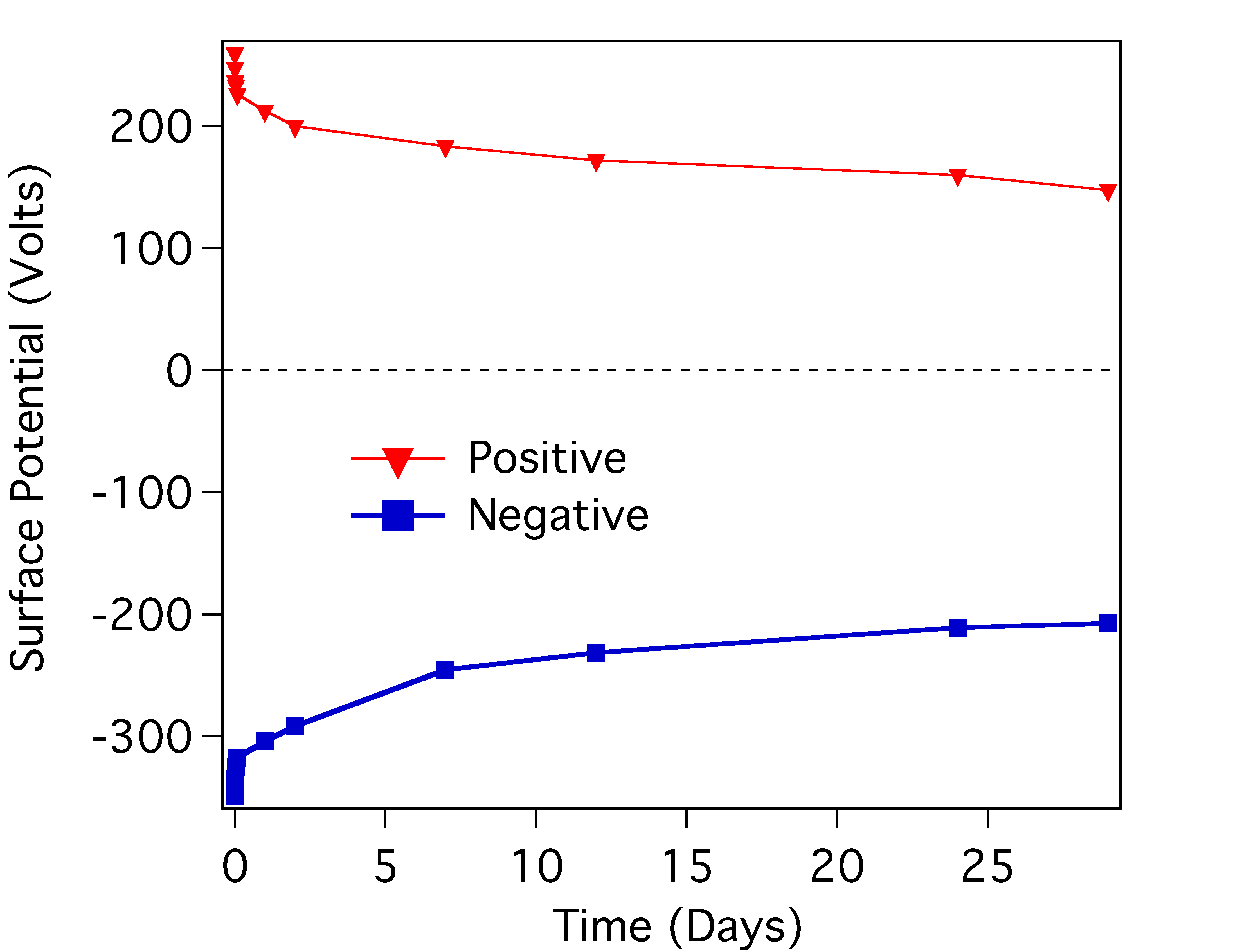 Figure 9
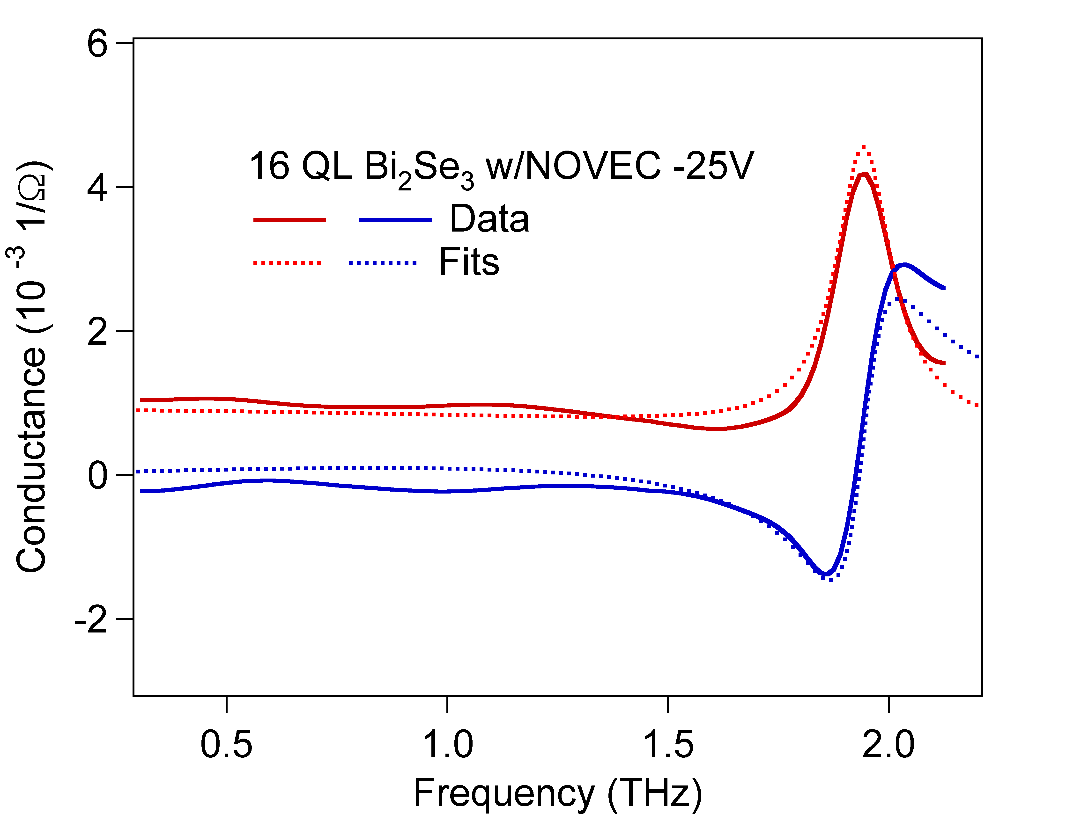 Figure 10
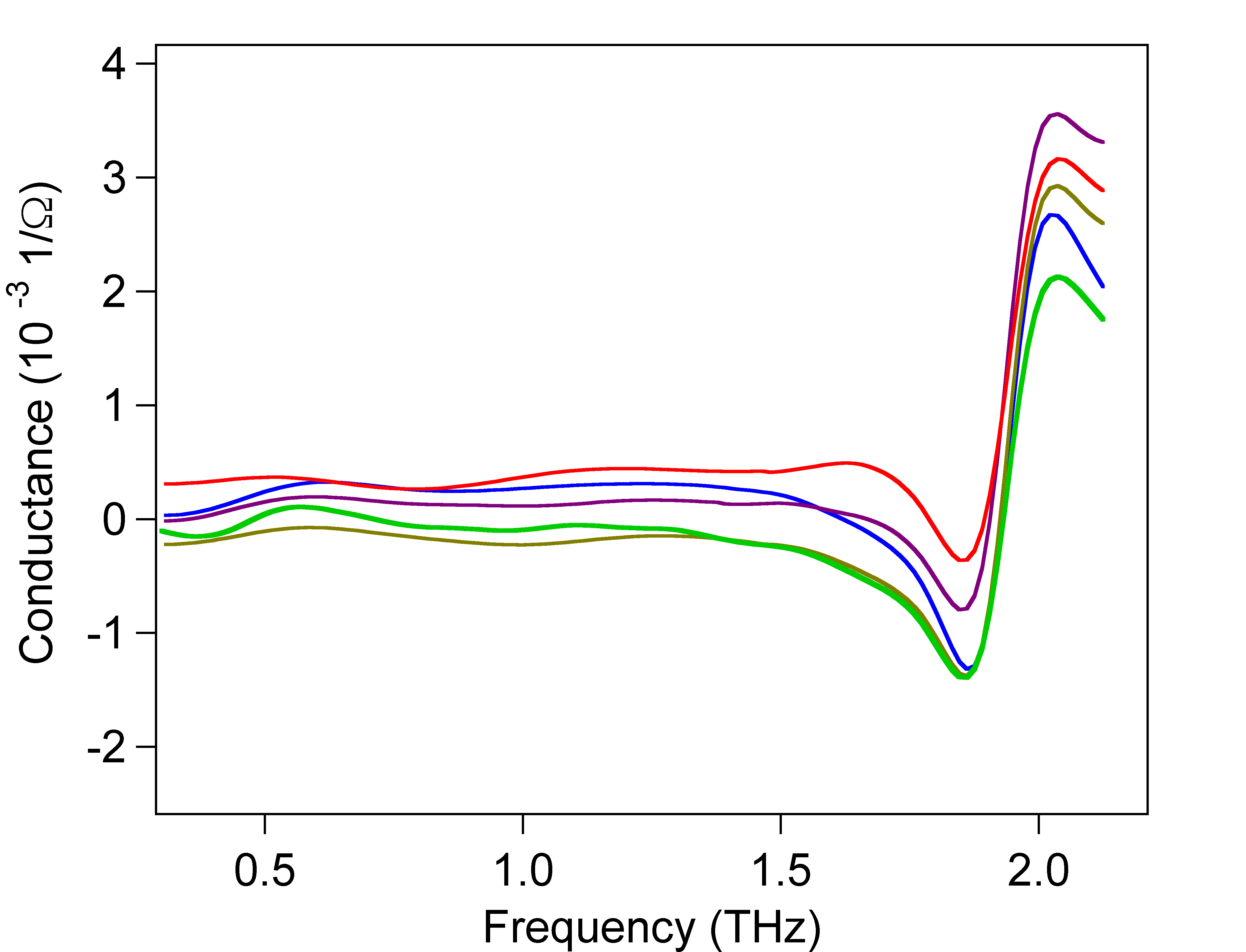 Figure 11
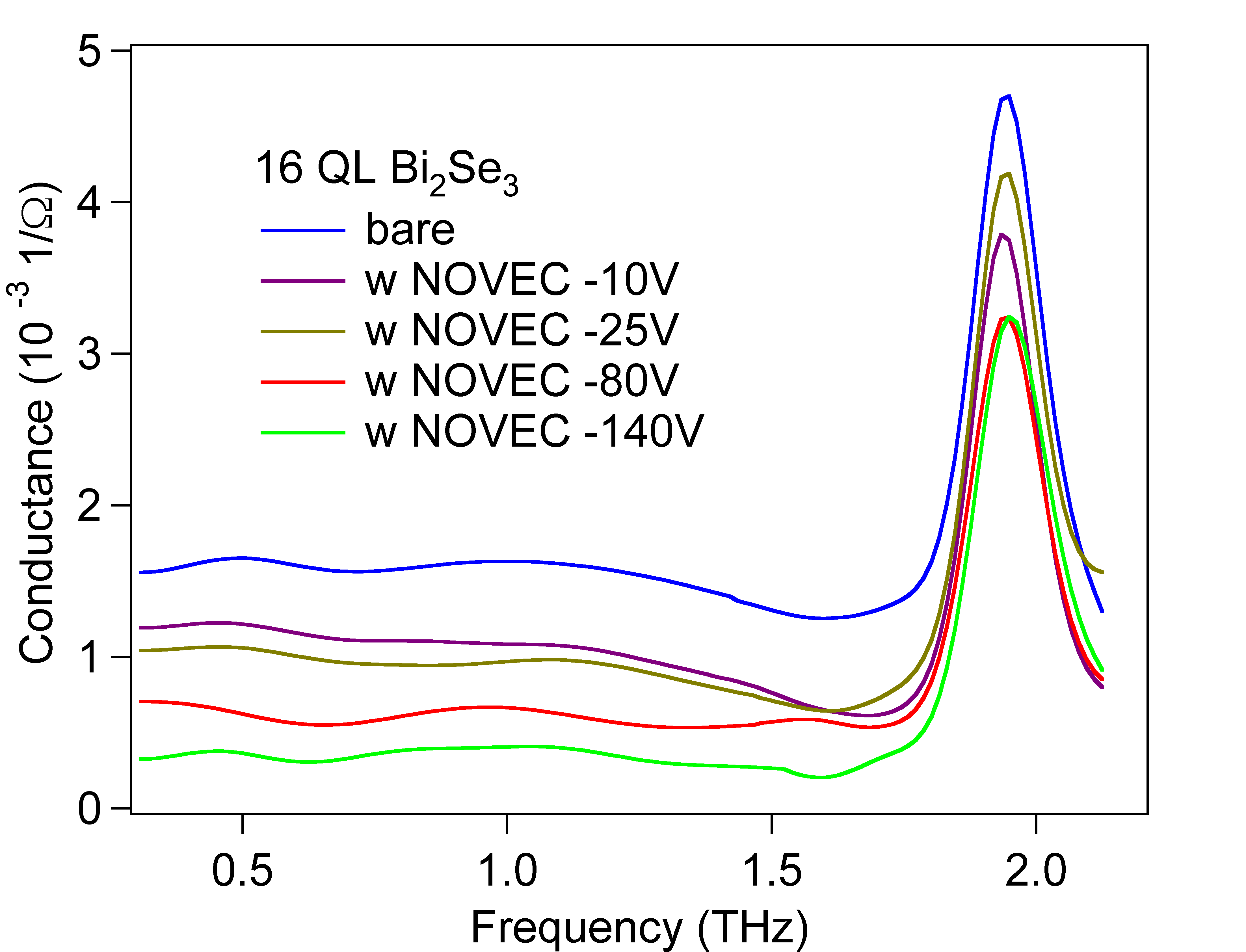 Figure 12
Peer Reviews
No public reviews on file for this paper yet. If you reviewed it on a platform where reviews are public (OpenReview, ICLR, NeurIPS, ICML), you can paste yours below so the community can read it here.
Videos
No videos yet. Explain this paper in a talk, walkthrough, or lecture? Add one.
Nonvolatile Solid-State Charged-Polymer Gating of Topological Insulators into the Topological Insulating Regime
R. M. Ireland
Department of Materials Science and Engineering and Department of Chemistry, The Johns Hopkins University, Baltimore, MD, USA 21218
Liang Wu
Department of Physics and Astronomy, The Johns Hopkins University, Baltimore, MD 21218, USA
M. Salehi
Department of Material Science and Engineering, Rutgers, The State University of New Jersey, Piscataway, NJ, 08854, USA
S. Oh
Department of Physics and Astronomy, Rutgers, The State University of New Jersey, Piscataway, NJ, 08854, USA
N. P. Armitage
Department of Physics and Astronomy, The Johns Hopkins University, Baltimore, MD 21218, USA
H. E. Katz
Department of Materials Science and Engineering and Department of Chemistry, The Johns Hopkins University, Baltimore, MD, USA 21218
Abstract
We demonstrate the ability to reduce the carrier concentration of thin films of the topological insulator (TI) Bi2Se3 by utilizing a novel approach, namely non-volatile electrostatic gating via corona charging of electret polymers. Sufficient electric field can be imparted to a polymer-TI bilayer to result in significant electron density depletion, even without the continuous connection of a gate electrode or the chemical modification of the TI. We show that the Fermi level of Bi2Se3 is shifted towards the Dirac point with this method. Using THz spectroscopy, we find that the surface chemical potential is lowered into the bulk band gap ( 50 meV above the Dirac point and 170 meV below the conduction band minimum) and it is stabilized in the intrinsic regime while enhancing electron mobility. This represents the first use of a charged polymer gate for modulating TI charge density. The mobility of surface state electrons is enhanced to a value as high as 1600 cm2/Vs at 5K.
I Introduction
Topological insulators (TIs) are a recently discovered class of materials, which support helical metallic surface states despite being (ideally) bulk insulators Hasan and Moore (2011); Hasan and Kane (2010); Qi and Zhang (2011). Unlike conventional surface states, their existence does not depend of the details of surface termination or environment, but only on certain properties of the underlying quantum mechanical wavefunctions. Examples of such materials are Bi1-xSbx, Bi2Se3, Bi2Te3, and TlBiSe2. The spin direction in the surface states is constrained to be in the plane of the surface and perpendicular to the momentum and therefore they exhibit suppressed backscattering when carrying a current. This novel spin structure may make TIs a novel platform for future low-dissipation spintronics applications Pesin and MacDonald (2012). Topological surface states may also display a host of interesting fundamental physics phenomena including a topological magneto-electric effect, quantized Faraday rotation and axion electrodynamics Maciejko et al. (2010); Qi et al. (2009). Early on, photoemission confirmed Hsieh et al. (2008); Chen et al. (2009); Hsieh et al. (2009) the existence of the surface states, however further development of the field hinges on controlling bulk electronic properties sufficiently to allow the surface properties to become dominant.
In this regard, the unique properties of TIs can only be fully realized in intrinsic (i.e. bulk-insulating) TIs. Reaching the intrinsic regime depends crucially on positioning the electrochemical potential in the bulk band gap. However an outstanding issue in this field is that most as-grown materials like Bi2Se3 typically have their chemical potential in the conduction band due to defect doping or band bending effects at surfaces, so their bulk properties are decidedly not insulating Analytis et al. (2010). This includes the high quality molecular beam epitaxy (MBE)-grown Bi2Se3 used in much of our own earlier workValdés Aguilar et al. (2012); Bansal et al. (2012); Valdés Aguilar et al. (2013); Wu et al. (2013). Although MBE is the most precise method Brahlek et al. (2011) for fabricating high quality Bi2Se3, most films prepared by this method will still have a high intrinsic n-type carrier concentration due to Se vacancies. In order to utilize the intrinsic TI physics, it is necessary to further deplete negative carriers.
Although there have been a number of recent advances Koirala et al. (2015); Wu et al. (2016a) in growing TIs with the chemical potential in the gap, further progress is needed to be able to tune the Fermi energy. Chemical potential manipulation may be achieved by means of a capacitively coupled gate electrode. For example, one may couple the gate electrode to the face of a two-dimensional inorganic sample via an ionic liquid Segawa et al. (2012); Shimizu et al. (2012); Yuan et al. (2011). This configuration, while indeed conveying a high capacitive field (up to 5 V across a molecular distance, 10 MV/cm) to the sample, suffers from a number of problems, including chemical inhomogeneity at the inorganic surface (a source of hysteresis and mobility-reducing scattering), limited control of parasitic capacitances and resistances, the possibility of electrochemistry at the inorganic sample surface, and an inability to confine the entire device structure to dimensions that would allow interference-free optical probing.
Some of these issues are ameliorated using solid gates. For example, ceramic Chang et al. (2015); Chen et al. (2010); Kim et al. (2012) gates have been used to observe changes in conductivity. However, this still requires connection and operation of a gate electrode to change the density during transport measurements. To avoid this, a few quasipermanent gating modifications have been made to TIs and related materials. For instance, it was shown that electron irradiation reversed the majority carrier sign in bismuth telluride Rischau et al. (2013). In a related demonstration to the current work, corona charging of graphene on silicon carbide tuned the charge density through the Dirac point Lartsev et al. (2014). Electron-accepting overlayers such as molybdenum trioxide and tetracyanoquinodimethane can be deposited adjacent to TIs Wu et al. (2016b). A recent work also utilized organics to engineer topological insulators, but they increase the Fermi energy and created Rashba surface states, which are topologically trivial Jakobs et al. (2015).
In this work, we demonstrate the ability to tailor the carrier concentration of Bi2Se3 films prepared by MBE by utilizing an approach without precedent in the TI field: nonvolatile electrostatic gating via the corona charging of electret polymers Giacometti et al. (1999). Sufficient electric field can be imparted to a polymer-TI bilayer to result in significant electron depletion without the continuous connection of a gate electrode or the chemical modification of the TI. We show that the Fermi level of Bi2Se3 is shifted towards the Dirac point by altering Bi2Se3 carrier concentrations with this method. We find that electrostatic gating is highly effective for lowering the surface chemical potential into the bulk band gap and stabilizing it in the intrinsic regime while enhancing electron mobility.
A corona discharge is an electrical discharge that occurs when a high voltage is applied between asymmetric electrodes such as a point and a plate. The emission or extraction of electrons induced by high voltage at the point creates gas-phase ions that move through a region in space, are brought to a defined potential by passing through a metal grid electrode set to that potential, and eventually become adsorbed onto or embedded near the surface of a polymer placed near the plate, a process that can be termed field-assisted adsorption. In contrast to techniques like electron-beam poling, in which electrons strike a surface with keV energies and penetrate into the bulk of the polymer, the energy of the corona ions is much smaller as they first move through the ambient atmosphere and then become equilibrated to the grid. The ions do not penetrate appreciably into the bulk of the materials, but instead transfer their charge to the surface where it resides or is injected into bulk traps as shown in Fig. 1 for negative charging, which results in depletion of a TI film. It has been used for applications in electrophotography, charging of electrostatic filters, and the poling of polymers to induce ferroelectricity and nonlinear optical effects Giacometti et al. (1999). In the present case we use it to charge a polymer electret and build-in a stable non-volatile electric field that can reduce the charge density of the TI surface states that are in contact with the polymer.
We selected commercially available or easily synthesized polymers: polystyrene (PS), polystyrene with 3 chloromethylstyrene comonomer (PS-Cl), polystyrene with 3 C60-methyl side chains (PS-C60)Alley et al. (2016) (made by direct substitution of the chloromethyl group with C60), and the perfluorinated polymer Novec. All four are highly hydrophobic, have wide electrochemical windows, and would be expected to have little or no chemical interaction with Bi2Se3. Polystyrene is a known electret/charge storage material, with demonstrated capability to tune semiconductor charge densities in a nonvolatile fashion. Dawidczyk et al. (2014, 2012); Erhard et al. (2010); Reuter et al. (2010). The chloromethylstyrene and C60-methylstyrene derivatives were investigated to see whether the labile chloro groups or additional fullerene energy levels would increase charge trapping relative to polystyrene. Novec is a non-ionic polymeric fluorochemical surfactant in a proprietary nonafluorobutyl ether that has not been used for the present purpose before, but as shown below, is particularly advantageous for the application under consideration.
II Experimental Details
Thin films in this study were 16 QL thick (1 QL is a unit cell and corresponds to 1 nm) low-carrier-density Bi2Se3 molecular beam epitaxy films grown on Bi2-xInxSe3 buffer layers grown on sapphire substrates using the Rutgers University custom-designed molecular beam epitaxy (MBE) system. Details are published elsewhere Koirala et al. (2015). DC measurements, photoemission spectroscopy, and THz experiments have shown no signatures of bulk or trivial two dimensional electron gas states Koirala et al. (2015). After growth, samples were sealed in vacuum bags and sent to Johns Hopkins University overnight.
Some polymers were drop-cast directly from solution onto substrates with premade Bi2Se3 films using about 0.1 ml of solution per square centimeter of substrate area. The polymer solvent is allowed to evaporate, resulting in polymer film thicknesses around 2-5 micrometers. Alternatively the films are spin-cast at 1000 rpm for 60 seconds in order to reduce the thickness and drying times. A single spin-cast layer is typically about 0.1 micrometers. Novec dries in a matter of minutes, whereas the polystyrene-based polymers are cast from chlorobenzene solutions diluted to 5 mg/ml, so drop-cast films may take more than 12 hours to dry in ambient atmosphere. As it dries quickly spin-cast Novec layers can be built up in repeated depositions, whereas polystyrene is too soluble to efficiently build up in this fashion. All films are further dried under low vacuum at 60∘ C for a couple of hours. The recommended environment for applying Novec coating is 20-27∘ C and 40-70 relative humidity to prevent moisture condensation on the polymer film and provide a reasonable drying time.
III Charging Studies
We performed a systematic study of conditions and materials that would allow the maximum static electric field to be stored in a polymer dielectric layer overlaying the Bi2Se3. Static charge was applied to the upper polymer surface via a metal screen (the “grid”) powered by a corona (plasma) emanating from a needle above the grid, establishing a potential of 10,000 volts between the needle and a grounded copper stage, as shown in Fig. 2. For some experiments, copper tape was used to connect the grounded stage to the Bi2Se3 in an attempt to set the Bi2Se3 semiconducting layers to ground as well. A triode arrangement with a grid is used to ensure greater uniformity of potential over the sample as previously demonstrated Giacometti et al. (1999). A grounded metal chamber encloses the entire apparatus, and is not removed when the needle or grid are powered. The stored voltage depended both on the charging time and grid voltage. The stored voltage was indicated by measuring with an electrostatic voltmeter. The electrostatic voltmeter is a surface DC voltmeter that measures surface potential in the range of 3000 V without physically contacting the measured surface. It features high-accuracy (0.1), drift-free measurements that are almost fully independent of probe-to-surface separation.
Charging was carried out in an ambient atmosphere for specific time periods and different grid voltages to determine the time evolution and maximum deposited static voltage for each multilayer. In Fig. 3a we show the surface charge voltage measured for polystyrene (PS), polystyrene with 3 chloromethylstyrene comonomer (PS-Cl), and polystyrene with 3 C60-methyl side chains (PS-C60) spin-coated onto a gold film. One can see that grounding increased the surface voltage that could be established. The stored surface potential saturates at a particular value for some grid voltage (in the tens of volts for 0.5 m thick spin-cast polymers). The time scales are consistent with a measured RC time constant of 20-150 seconds for the polymer films. Conclusions drawn from this are that both of the functionalized side chains contributed to the charge storage ability, about half of the maximum voltage that could be stored across the entire sample could be localized between the top and bottom polymer surfaces. About one third more voltage could be maintained if the sample were heated to 80∘ C during charging. As shown in Fig. 3b Novec had even better properties in holding charge than PS-Cl. There one can see that with -1500 V applied grid voltage as comparing PS-Cl Novec deposited on Bi2Se3 clearly showed superior abilities to charge to larger voltages and in shorter times. We speculate that as Novec is fluorinated and otherwise lacking in polar functional groups, any sites in which free electrons or holes can be trapped are highly stabilized against being quenched by environmental water molecules and also have such high-barrier migration pathways that they are not easily discharged.
Given its superior properties, we proceeded to do an in-depth study of the capacity of Novec to store charge and exhibit a stable surface potential on TIs. Fig. 4 shows various tests for the long term stability of the stored potential in Novec. Fig. 4a shows the surface potential after charging at constant grid voltage as a function of time. Fig. 4b shows the resulting potential stored in Novec after charging for a fixed time (5 minutes) at incremental grid voltages. Fig. 4c shows the resulting potential stored in Novec after charging at single high grid voltage and then monitoring the stability of stored charge as a function of time (samples left in air) over the course of almost one month. One can see that Novec exhibits excellent properties in terms of large voltages that can be stored over long time scales.
IV Effectiveness in modifying charge conduction
The complex conductivity was determined by time-domain THz spectroscopy (TDTS). A femtosecond laser pulse is split along two paths and excites a pair of photoconductive ‘Auston’-switch antennas. A broadband THz range pulse is emitted by one antenna, transmitted through the TI film, and measured at the other antenna. By varying the length-difference between the two paths, one uses the split off laser beam to optically gate the second switch and map out the entire electric field of the transmitted pulse as a function of time. Taking the ratio of the Fourier transform of the transmission through the TI on a substrate to that of a bare substrate gives the complex transmission function. We then invert the transmission to obtain the complex conductivity via the standard formula for thin films on a substrate: where is the index of refraction of the sapphire substrate. By measuring both the magnitude and phase of the transmission, this inversion to conductivity is done directly and does not require Kramers-Kronig transformation. As a characterization tool TDTS has the advantages of being non-destructive and non-contact. Moreover it accesses the conventionally difficult to utilize THz part of the electromagnetic spectrum.
We demonstrate the effectiveness of a monolithic single-component charged electret in extracting charge carriers from bismuth selenide utilizing THz measurementsWu et al. (2016b). In the THz spectra in Fig. 5, there is a Drude component peaked at zero frequency and a phonon peak at 1.9 THz as observed extensively previously Valdés Aguilar et al. (2012); Wu et al. (2016b, 2013). These features manifest themselves in both the real and imaginary parts of the conductivity. As done previously, we fit these spectra to a model where we fit the spectra to a Drude peak, a Drude-Lorentz peak for the phonon and a term that accounts for the polarizability of the lattice. The area of the peak assigned to the Drude conductance is proportional to carrier density over effective mass. Therefore Drude peaks with lower area means lower carrier density. We fit both the real and imaginary parts of the conductance simultaneously to a Drude transport model. Using the known band structure of Bi2Se3 Wu et al. (2016b); Wu, Liang and Tse, Wang-Kong and Brahlek, M. and Morris, C. M. and Aguilar, R. Valdes and Koirala, N. and Oh, S. and Armitage, N. P. (2015), we can extract out the carrier density and also the chemical potential. It is reasonable to assume that the charge polymer layer does not modify the essential aspects of the band structure as it is spin coated on and not bonded in any fashion.
We found that Bi2Se3 with a negatively charged polymer layer has the smallest conductance area and the positively charged one barely changes the conductance, indicating that negatively charged polymers deplete the carrier density of surface states of Bi2Se3 while the positive one slightly increases the carrier density. This polarity is consistent with charge stored as a dipole, with one pole in the dielectric and the other pole in the Bi2Se3 or at its polymer interface, where electrons would be trapped (Fig 1). In Fig. 6 we can see that immediately upon spin coating, the charge density of the Bi2Se3 film falls and we found that Novec usually automatically traps -10 V. It is possible that Novec introduces an interface dipole that itself depletes some charges, or counteracts some pre-existing surface dipole or chemical species that stabilizes a certain quantity of charge in the uncoated TI sample.
Charging was done under grounding conditions. For large positive applied charges, the charge density increases slightly, but for negative charges the density decreases dramatically. Using the known band structure, the chemical potential of the film as a function of the charging potential can be derived Wu, Liang and Tse, Wang-Kong and Brahlek, M. and Morris, C. M. and Aguilar, R. Valdes and Koirala, N. and Oh, S. and Armitage, N. P. (2015); Wu et al. (2016b). For the largest charging potentials, the chemical potential can be tuned to within 50 meV of the Dirac point. By using the band dispersion and measuring the Drude transport life time in THz conductivity, we can estimate the mobility at 5 K is 1600 cm2/Vs at 5K. We repeated charging experiments on three spin-coated Novec-Bi2Se3 samples and observed voltage dependence as the one shown in Fig. 5. We also measured two Bi2Se3 samples with drop-cast Novec a few micrometer thick and saw similar behavior. For such samples we observed similar depletion, but because the analysis is more complicated due to the optically thicker polymer layer, we show here only the spin-coated results.
V Conclusions
We have demonstrated the ability to reduce the carrier concentration of thin films of the topological insulator (TI) Bi2Se3 by utilizing a novel approach, namely non-volatile electrostatic gating via corona charging of electret polymers. We demonstrate that a perfluorinated electret polymer is a highly effective static gate material to modulate topological insulator charge density. Sufficient electric field can be retained by this polymer to accomplish significant electron depletion of Bi2Se3, shifting the Fermi level towards the Dirac point and lowering the surface chemical potential into the bulk band gap. The Bi2Se3 is stabilized in the intrinsic regime while its electron mobility is enhanced. Our work represents the first use of a charged polymer gate for modulating TI charge density.
VI Acknowledgements
The topological insulator preparation and physical study was supported by NSF DMR-1005398 with additional support to SO by a Gordon and Betty Moore Foundation, EPiQS Initiative Grant GBMF4418. The charged polymer selection, process development, and characterization were supported by the Department of Energy, Office of Basic Energy Sciences, Grant Number SPACE DE-FG02-07ER46465.. RMI and LW contributed equally to this work.
The reference list from the paper itself. Each links out to its DOI / PubMed record.
- 1Hasan and Moore (2011) M. Zahid Hasan and Joel E. Moore, “Three-dimensional topological insulators,” Ann. Rev. Cond. Mat. Phys. 2 , 55 (2011).
- 2Hasan and Kane (2010) M. Z. Hasan and C. L. Kane, “ Colloquium : Topological insulators,” Rev. Mod. Phys. 82 , 3045 (2010).
- 3Qi and Zhang (2011) Xiao-Liang Qi and Shou-Cheng Zhang, “Topological insulators and superconductors,” Rev. Mod. Phys. 83 , 1057–1110 (2011).
- 4Pesin and Mac Donald (2012) Dmytro Pesin and Allan H Mac Donald, “Spintronics and pseudospintronics in graphene and topological insulators,” Nature materials 11 , 409–416 (2012).
- 5Maciejko et al. (2010) Joseph Maciejko, Xiao-Liang Qi, Andreas Karch, and Shou-Cheng Zhang, “Fractional topological insulators in three dimensions,” Phys. Rev. Lett. 105 , 246809 (2010).
- 6Qi et al. (2009) Xiao-Liang Qi, Rundong Li, Jiadong Zang, and Shou-Cheng Zhang, “Inducing a magnetic monopole with topological surface states,” Science 323 , 1184–1187 (2009).
- 7Hsieh et al. (2008) D. Hsieh, D. Qian, L. Wray, Y. Xia, YS Hor, RJ Cava, and MZ Hasan, “A topological Dirac insulator in a quantum spin Hall phase,” Nature 452 , 970–974 (2008).
- 8Chen et al. (2009) Y. L. Chen, J. G. Analytis, J.-H. Chu, Z. K. Liu, S.-K. Mo, X. L. Qi, H. J. Zhang, D. H. Lu, X. Dai, Z. Fang, S. C. Zhang, I. R. Fisher, Z. Hussain, and Z.-X. Shen, “Experimental Realization of a Three-Dimensional Topological Insulator, Bi 2 Te 3 ,” Science 325 , 178–181 (2009) . · doi ↗