Comment on “Dependence of Performance of Si Nanowire Solar Cells on Geometry of the Nanowires”
Joondong Kim

Abstract
Genes, proteins, chemicals, diseases, species, mutations and cell lines named across the full text — each resolved to its canonical identifier and authoritative record.
Click any figure to enlarge with its caption.
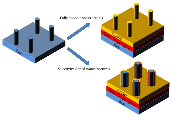 Figure 1
Peer Reviews
No public reviews on file for this paper yet. If you reviewed it on a platform where reviews are public (OpenReview, ICLR, NeurIPS, ICML), you can paste yours below so the community can read it here.
Videos
No videos yet. Explain this paper in a talk, walkthrough, or lecture? Add one.
Taxonomy
TopicsNanowire Synthesis and Applications · Silicon and Solar Cell Technologies · Thin-Film Transistor Technologies
A recently published report, titled “Dependence of Performance of Si Nanowire Solar Cells on Geometry of the Nanowires,” has systematically investigated Si structural effects on Si solar cells [1]. According to the report, a significant reduction of optical reflection (~1%) was achieved by using nanoscale-patterned Si structures, which has been realized by metal-assisted wet etching method.
The suppression of reflection on a Si surface may provide the enhanced absorption of the incident light into the light-reactive semiconductor (Si) material and, therefore, could directly improve the solar cell performances. The practical results, however, showed the deviation between the optical absorption and the electrical improvements. We may find this discrepancy from the diode characteristics of nanoscale-patterned photoelectric devices. With smaller Si structures, the Si surface area is proportionally increased along with the patterned Si. Meanwhile, direct etching of Si would drastically induce defect formation on the Si surface, which has been reflected on the higher reverse saturation current density and ideality factor values in the report.
Is it possible to realize the optical benefits into the electrical enhancements? We should reconsider the basic and important rules to resolve it. A solar cell is a device to convert the light energy into the electric energy, which is the only device to produce electric power from the light to date, different from the electric power consumption devices to produce light emission, such as LEDs, displays, and lightings. All these photoelectric devices are based on the diode operation, which has a rectifying current flow due to the potential barrier-junction formation between two work function-different materials. By contacting work function-different materials, major carriers diffused to the counterpart side to establish a space charge region (SCR) in which an electric field exists [2]. The electric field is a driving force to collect the photogenerated carriers, and thus the SCR employment is crucial factor for solar cell performances. Due to the lack of moving carriers (less recombination concern) inside of SCR, the collection efficiency of photogenerated carriers in SCR is ideally perfect. This is a strong clue of functional designs for highly efficient solar cells. The SCR length directly affects the light-active area of collection for photogenerated carriers.
In the report [1], Si nanowire- (SiNW-) embedding structure was doped by spin-on dopant method. Considering the conventional doping profiles, the emitter doping layer formed in several-hundred-nanometer depth from a surface [2]. This means that ~100 nm diameter size SiNWs were entirely doped, resulting in the junction formation of SiNWs (emitter) and a bottom Si substrate (base) to give no effect for SCR surface enlargement. This can be one of the reasons for low electrical performance enhancement from the optical benefits of SiNWs.
To achieve the proportional SCR elongation along the nanostructure, a fine doping process, such as ion implantation [3], is highly required to establish the junction inside the nanoscale feature as presented in Figure 1. Additionally, patterning of semiconductor almost always brings the surface defects to cause serious recombination problems. To qualify the junction formation, optically functional designs can be considered. A transparent nanoscale-pattern can be employed onto planar solar cells to separate the optical benefits from the defect-driven electric recombination loss [4]. In case of direct pattering of semiconductor materials, a passivation layer should be applied to coat the patterned semiconductor surface to suppress the defect concerns [3, 5, 6].
The reference list from the paper itself. Each links out to its DOI / PubMed record.
- 1Khan F.Baek S.-H.Kim J. H.Dependence of performance of Si nanowire solar cells on geometry of the nanowires The Scientific World Journal 20142014735840810.1155/2014/3584082-s 2.0-84893821337 PMC 391555224574884 · doi ↗ · pubmed ↗
- 2Kim H.Kim J.Lee E.Kim D.-W.Yun J.-H.Yi J.Effect of the short collection length in silicon microscale wire solar cells Applied Physics Letters 20131021919390410.1063/1.48045812-s 2.0-84877996122 · doi ↗
- 3Ur Rehman A.Lee S. H.Advancements in n-type base crystalline silicon solar cells and their emergence in the photovoltaic industry The Scientific World Journal 201320131347034710.1155/2013/4703472-s 2.0-84896387032 PMC 389123024459433 · doi ↗ · pubmed ↗
- 4Yun J. H.Lee E.Park H. H.Incident light adjustable solar cell by periodic nanolens architecture Scientific Reports 20144, article 687910.1038/srep 06879 PMC 422028325371099 · doi ↗ · pubmed ↗
- 5Kim J.Yun J.-H.Kim H.Transparent conductor-embedding nanocones for selective emitters: optical and electrical improvements of Si solar cells Scientific Reports 20155, article 925610.1038/srep 09256 PMC 436540025787933 · doi ↗ · pubmed ↗
- 6Mahalingam S.Abdullah H.Shaari S.Muchtar A.Asshari I.Structural, morphological, and electron transport studies of annealing dependent In 2O 3 dye-sensitized solar cell The Scientific World Journal 201520151040384810.1155/2015/403848 PMC 447142226146652 · doi ↗ · pubmed ↗