A Dual-Band Filter Using a Multimode Resonator with Asymmetrically Loaded Open-Circuited Stubs for Independent Passband Control
Qun Chen, Li Zhang, Liqin Liu

TL;DR
This paper presents a new dual-band filter design for 5G systems using a resonator with open-circuited stubs to control two passbands independently.
Contribution
The novel multimode resonator design enables independent dual-band control with high selectivity and isolation for 5G applications.
Findings
The filter achieves a 2.6 GHz passband with 13.7 dB return loss and 0.37 dB insertion loss.
A second passband at 4.8 GHz shows 23.6 dB return loss and 0.77 dB insertion loss.
The design provides three transmission zeros for high selectivity and isolation in 5G systems.
Abstract
A novel multimode resonator is designed in this paper. Incorporating two open-circuited stubs of distinct impedances loaded onto a uniform half-wavelength transmission line, the resonator enables the realization of a dual-band filter—with center frequencies at 2.6 GHz and 4.8 GHz—through both simulation and experimental measurement. Regarding the first passband centered at 2.6 GHz, the device exhibits a return loss |S11| of 13.7 dB, an insertion loss |S21| of 0.37 dB, and a 3 dB bandwidth of 17.3%. As for the second passband with a center frequency of 4.8 GHz, the measured return loss |S11| amounts to 23.6 dB, the insertion loss |S21| measures 0.77 dB, and the 3 dB bandwidth is recorded at 8.75%. Specifically designed for 5G communication systems, the filter achieves three transmission zeros by adopting electrical coupling and 0° feeding, resulting in high selectivity and high…
Click any figure to enlarge with its caption.
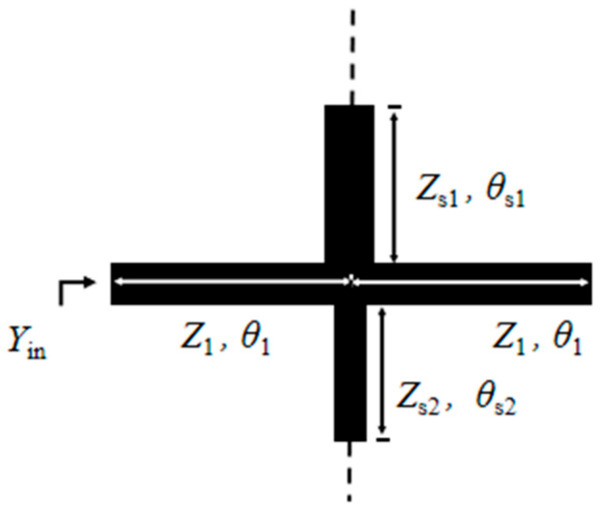 Figure 1
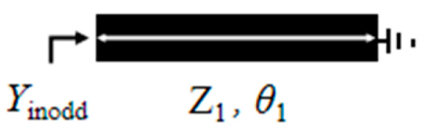 Figure 2
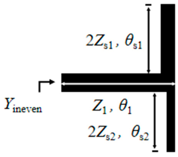 Figure 3
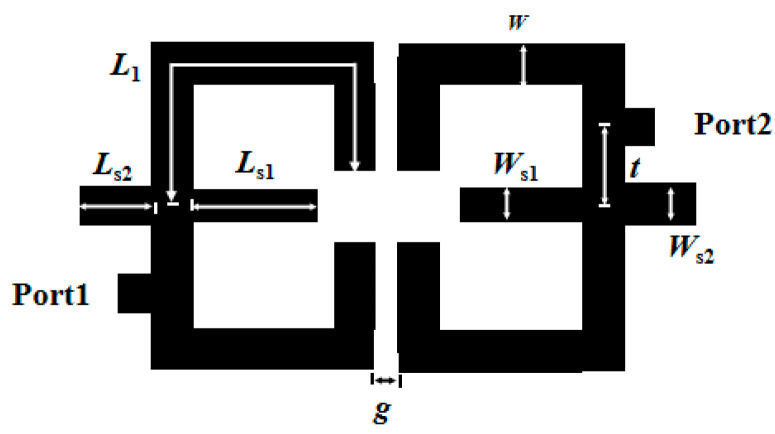 Figure 4
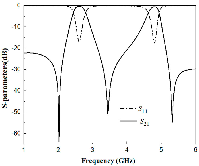 Figure 5
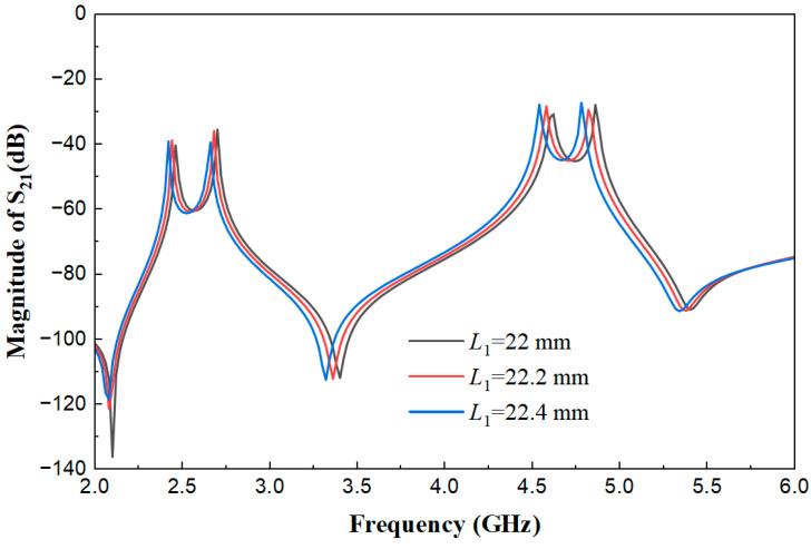 Figure 6
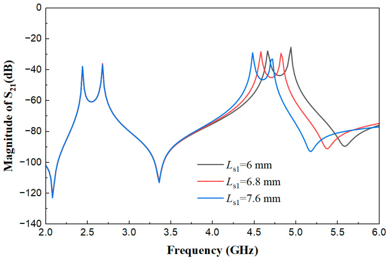 Figure 7
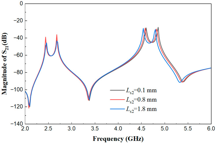 Figure 8
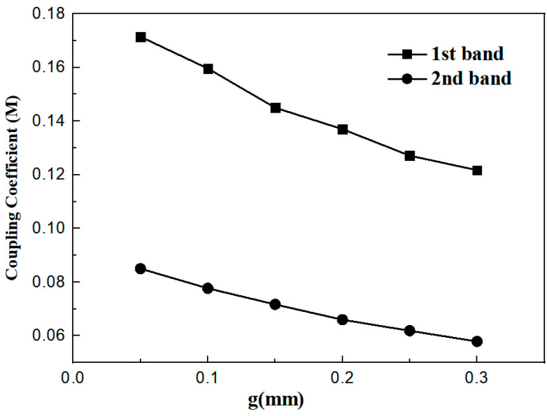 Figure 9
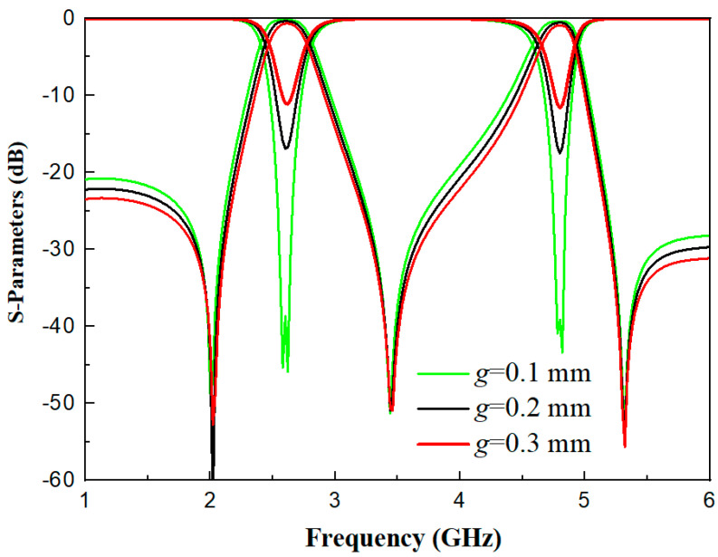 Figure 10
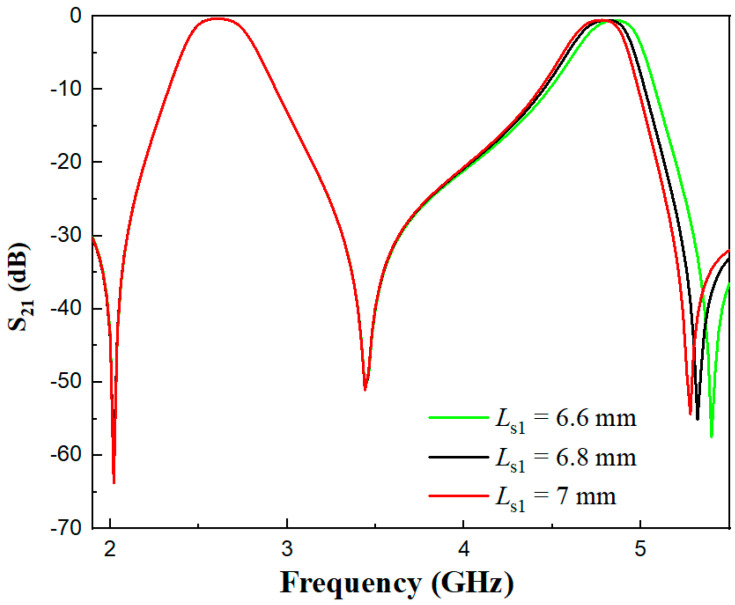 Figure 11
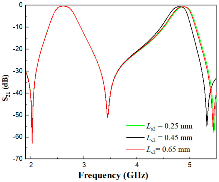 Figure 12
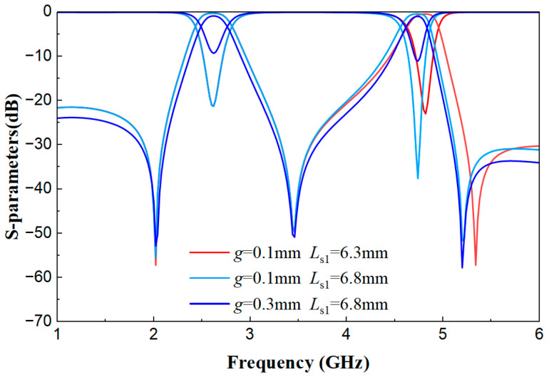 Figure 13
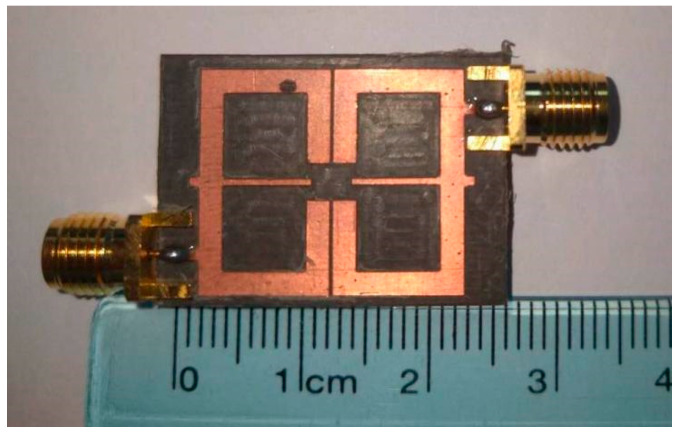 Figure 14
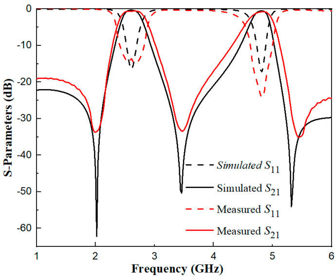 Figure 15
- —Natural Science Foundation of Fujian Province
- —Putian University Scientific Research Project
- —Electronic Information Industry Technology Research Institute of Putian
Peer Reviews
No public reviews on file for this paper yet. If you reviewed it on a platform where reviews are public (OpenReview, ICLR, NeurIPS, ICML), you can paste yours below so the community can read it here.
Videos
No videos yet. Explain this paper in a talk, walkthrough, or lecture? Add one.
Taxonomy
TopicsMicrowave Engineering and Waveguides · Antenna Design and Analysis · Metamaterials and Metasurfaces Applications
1. Introduction
Amid the fast-paced evolution of information and communication technologies, wireless communication systems have achieved notable advancements. As a crucial component in mobile communication systems, filters are primarily responsible for frequency selection during signal transmission and reception at the transmitter and receiver, thereby filtering out interference and clutter signals. At the same time, spectral resources are growing progressively scarce. To enhance the utilization efficiency of such resources, the design of multi-band filters—including dual-band filters [1,2,3], tri-band filters, and quad-band filters [4,5,6,7]—has become increasingly crucial.
Conventional multi-band filters are constructed by cascading several single-band filters, which necessitates matching components such as duplexers. This not only adds to the system’s complexity but also increases its physical dimensions. In contrast, the use of dual-band filters can reduce system volume and minimize losses. In recent years, various methods have been proposed for designing dual-band filters. In [8], a balanced dual-band filter is designed using resonators composed of two identical folded third-order stepped impedance resonators (TSIRs). In [9], an independently reconfigurable dual-band filter based on stub-loaded multimode resonators is proposed. By analyzing the operating modes of the stepped impedance resonator (SIR), the optimal positions of the loaded stubs and varactors are determined, and a 0° feeding structure is introduced, ultimately achieving bandpass filtering functionality with independently reconfigurable center frequencies of the dual passbands. In [10], a novel microstrip switchable bandpass filter (BPF) is presented. The topology realizes three filtering mode switches (broadband bandpass filter, dual-band bandpass filter, and tri-band bandpass filter) by controlling the on-off state of radio frequency PIN diodes. In [11], a dual-band microstrip bandpass filter with a unique structure is designed, adopting broadside coupling technology and a feeding method based on a 50 Ω coplanar waveguide, achieving a compact structure, narrow fractional bandwidth, and low insertion loss. In [12], a self-coupled resonant cavity composed of asymmetric parallel microstrip transmission lines is proposed, and a dual-band bandpass filter with a wide stopband is designed and implemented. In [13], a design of a center-loaded stub stepped impedance resonator based on a T-type resonator is proposed, and a fourth-order dual-band bandpass filter is realized on a double-sided YBCO high-temperature superconducting thin film with excellent performance. While it achieves low IL (0.41/0.65 dB after scaling), HTS fabrication is costly and requires cryogenic operation, limiting practicality. In [14], a compact SIW-based dual-band filter is proposed, suitable for high-frequency integration but with limited fractional bandwidth. In [15], an interdigital filter achieves high selectivity in the C-band, yet its design lacks independent passband tunability. In [16], a dual-band filter with reflectionless characteristics and enhanced stopband suppression is presented. While their design excels in out-of-band reflection absorption, it employs a more complex topology with additional matching networks. In contrast, our proposed resonator provides independent control of both passbands through adjustable stub parameters, achieves low loss on standard PCB, and maintains a compact footprint suitable for 5G front-end modules.
In this paper, a multimode resonator is designed, which consists of a uniform half-wavelength transmission line loaded with two open-circuited stubs of different impedances at symmetric central positions. The proposed filter possesses excellent out-of-band rejection capability and demonstrates performance advantages compared to other similar filters. This paper analyzes the resonance characteristics of the multimode resonator and verifies the feasibility of the parameter mechanism of “overall tuning by the main stub + targeted regulation by the auxiliary stubs”.
2. Design and Analysis of the Resonator
2.1. Structure of the Multimode Resonator
The structure of the novel multimode resonator is shown in Figure 1. It consists of a uniform half-wavelength transmission line loaded with two open-circuited short stubs at upper and lower symmetric central positions. The impedance and electrical length of the uniform half-wavelength transmission line are defined as Z1 and θ1, respectively. The impedance and electrical length of the upper stub are Zs1 and θs1, while those of the lower stub are Zs2 and θs2.
2.2. Resonance Analysis of the Resonator
Define the impedance ratio K1 as K1 = Zs1/Z1 and K2 as K2 = Zs2/Z1. Based on transmission line theory, the input admittance Y_in_ of the resonator can be derived. The solutions satisfying the condition Y_in_ = 0 correspond to the resonant modes of the resonator. Figure 2 presents the odd-mode structure diagram of the novel multimode resonator, and Figure 3 shows the even-mode structure diagram. Based on the odd-even mode analysis method in transmission line theory [16], the resonance conditions corresponding to the odd-mode and even-mode resonances of the novel multimode resonator can be expressed as follows:
The resonator has three electrical lengths: θ1, θs1, and θs2. Define the electrical length ratios α_1_ and α_2_. As α_1_ = 2θs1/θ_T_ and α_2_ = 2θs2/θT, where θT is the total electrical length of the uniform half-wavelength transmission line (θT = 2θ1). Substituting the two electrical length ratios into Equations (1) and (2), the resonance conditions corresponding to the odd-mode and even-mode resonances are obtained as follows:
It can be observed from Equation (3) that the odd-mode resonant frequency of the proposed resonator is independent of the loaded stubs. From Equation (4), the even-mode resonant frequency is related to the electrical lengths θs1 and θs2 of the loaded stubs. Therefore, this characteristic can be utilized to design a frequency-controllable dual-band microstrip bandpass filter. The design concept is: first, adjust the odd-mode resonant frequency to the desired operating frequency, and then tune the even-mode resonant frequency to the target value by modifying the structural parameters of the two stubs. Compared with the traditional SIR, the proposed resonator has more structural parameters affecting the resonance conditions, leading to a significant improvement in design flexibility and the ability to independently adjust the resonant frequencies of the two passbands.
3. Filter Design and Parameter Optimization
3.1. Filter Structure
To further verify the above analysis, a dual-band microstrip bandpass filter is designed using the aforementioned multimode resonator. Electrical coupling is adopted as the coupling method for the filter, and a tapped line feeding method is employed. Out-of-band rejection is a crucial performance indicator of filters, so transmission zeros are introduced to enhance out-of-band rejection. Through the selected electrical coupling structure and tapped 0° feeding method, combined with simulation analysis and parameter optimization using IE3D15 software, the structure diagram of the dual-band microstrip bandpass filter based on the multimode resonator is finally obtained, as shown in Figure 4. Both simulation and measurement of the proposed filter were conducted on an RT/Duroid 5880 substrate, which is characterized by a thickness of 0.787 mm, a relative dielectric constant (ε_r_) of 2.2, and a loss tangent of 0.0009.
By adjusting the electrical length ratios of the upper and lower stubs, the dual-band filter is realized. Figure 5 shows the performance diagram of the dual-band filter obtained through HFSS simulation, with center frequencies of 2.6 GHz and 4.8 GHz. The simulation parameters of the filter are as follows: L1 = 22.2 mm, W = 1.8 mm, Ws1 = 0.45 mm, Ls1 = 6.8 mm, Ls2 = 0.8 mm, Ws2 = 0.7 mm, t = 5.5 mm and g = 0.2 mm. For the first passband (center frequency: 2.6 GHz), the return loss |S11| is 16.3 dB, the insertion loss |S21| is 0.358 dB, and the 3 dB bandwidth is 13.96%. For the second passband (center frequency: 4.8 GHz), the return loss |S11| is 16.8 dB, the insertion loss |S21| is 0.558 dB, and the 3 dB bandwidth is 6.7%. Due to the combined effect of the electrical coupling structure and 0° feeding adopted in the design, three transmission zeros are generated at frequencies of 2.02 GHz, 3.44 GHz, and 5.31 GHz, achieving high selectivity.
3.2. Weak Coupling Analysis of Each Stub
Figure 6 shows the weak coupling effect diagrams of the multimode resonator when L1 is 22 mm, 22.2 mm, and 22.4 mm, with other parameters fixed (Ws1 = 0.45 mm, Ls1 = 6.8 mm, Ls2 = 0.8 mm, Ws2 = 0.7 mm, W = 1.8 mm, t = 5.5 mm, g = 0.2 mm). It can be observed from Figure 6 that as the main resonant length L1 increases from 22 mm to 22.4 mm, all resonant modes of the resonator shift uniformly towards lower frequencies, while the frequency spacing between modes and the coupling strength remain relatively stable. This indicates that L1, as the main resonant length of the resonator, primarily functions to globally control the positions of the fundamental frequency and each harmonic frequency, providing a foundation for the precise tuning of the center frequencies of the dual-band filter.
Figure 7 presents the weak coupling effect diagrams of the multimode resonator when Ls1 is 6 mm, 6.8 mm, and 7.6 mm, with other parameters fixed (Ws1 = 0.45 mm, L1 = 22.2 mm, Ls2 = 0.8 mm, Ws2 = 0.7 mm, W = 1.8 mm, t = 5.5 mm, g = 0.2 mm). As shown in the figure, when Ls1 is 6 mm, 6.8 mm, and 7.6 mm, the characteristics of the low-frequency resonant peak near 2.5 GHz do not change significantly, but the overlap degree and amplitude distribution of the high-order resonant peaks near 5 GHz change obviously. This indicates that Ls1 is a key parameter for targeted regulation of the multimode coupling matching state in the high-frequency band.
Figure 8 displays the weak coupling effect diagrams of the multimode resonator when Ls2 is 0.1 mm, 0.8 mm, and 1.8 mm, with other parameters fixed (L1 = 22.2 mm, W = 1.8 mm, Ws1 = 0.45 mm, Ls1 = 6.8 mm, Ws2 = 0.7 mm, t = 5.5 mm, g = 0.2 mm). It can be seen from Figure 9 that the variation in the coupling segment Ls2 mainly affects the high-frequency resonant mode (near 5.0 GHz), and its function is similar to that of Ls1 but acts on different high-frequency resonant points. This indicates that Ls1 and Ls2 are jointly responsible for the independent regulation of different resonant modes within the high-frequency band.
This parameter mechanism of “overall tuning by the main stub + targeted regulation by the auxiliary stubs” endows the resonator with flexible regulation capability of multimode characteristics, providing a reliable basic unit for the multi-frequency characteristic design of dual-band filters.
3.3. Coupling Coefficient
In this paper, two novel multimode resonators are electrically coupled to realize a dual-band bandpass filter with center frequencies of 2.6 GHz and 4.8 GHz, respectively. The 3 dB fractional bandwidths (FBW) of the two passbands are 13.96% and 6.7%, respectively. The lumped circuit element values of the corresponding low-pass prototype filter are: g1 = 0.90467 and g2 = 1.25868, where gn (n = 1 to 2) are the element values [16]. The theoretical coupling coefficient and external quality factor can be obtained by the following formulas [17]:
Substituting the bandwidths, g_1_, and g_2_ values of the two passbands into Equations (5) and (6), the following results are obtained:
The external quality factor of the first passband is , and that of the second passband is .
Studies have shown that t influences the external quality factor, and the value of the coupling coefficient related to the desired fractional bandwidth is determined by the coupling gap (g). In addition, the coupling coefficient can be calculated through the transmission coefficient obtained from full-wave simulation [17], and its expression is as follows:
where fH and fL are defined as the frequencies corresponding to the higher-order mode and lower-order mode among the two resonant modes, respectively, and f1 is the resonant frequency. As can be seen from Figure 9, as the value of g increases, the value of the coupling coefficient decreases. In this paper, g is set to 0.2 mm because the minimum precision of the laboratory engraving machine is 0.2 mm. Figure 10 shows the comparison diagram of S-parameters under different g values. It can be observed that as g decreases, the insertion loss |S21| decreases, while the return loss increases.
3.4. Influence of Two Open-Circuited Stubs on Filter Performance
As can be seen from Figure 11 and Figure 12, the two open-circuited stubs Ls1 and Ls2 have no influence on the first passband, which verifies Equation (3) that the odd-mode resonant frequency is independent of the two stubs. In the even-mode analysis, Equation (4) is a function of the electrical length ratios α1 and α2 and impedance ratios. With fixed impedance ratios, the even-mode resonance depends on the electrical length ratios. It can be observed from Figure 11 that as Ls1 increases, the center frequency of the second passband decreases. Figure 12 shows that Ls2 plays a fine-tuning role in the center frequency of the second passband.
Figure 13 is shown below. When g = 0.1 mm (strong coupling), increasing Ls1 from 6.3 mm to 6.8 mm improves the S21 performance of the second passband. When switching from strong coupling (g = 0.1 mm) to weak coupling (g = 0.3 mm) while keeping Ls1 unchanged, the S11 and S21 performance of both passbands deteriorates.
By summarizing Section 3.1, Section 3.2, Section 3.3 and Section 3.4 content, we can derive the sensitivity (analysis results):
- (1)L1 (Main Transmission Line Length): It has the highest sensitivity to the center frequencies of the dual passbands and serves as a global core parameter. It must be fixed first to ensure a stable frequency baseline.
- (2)g (Coupling Gap): It has the second-highest sensitivity to coupling strength and insertion loss, directly determining the passband matching foundation. It should be optimized after L1 is fixed.
- (3)Ls1 (Upper Open-Circuited Stub Length): It has extremely high sensitivity to the insertion loss optimization of the high-frequency passband and acts as a core fine-tuning parameter for the performance of the high-frequency passband.
- (4)Ls2 (Lower Open-Circuited Stub Length): It has the lowest sensitivity and is only used for fine calibration of the high-frequency passband, with a limited impact on overall performance.
3.5. Procedure for Calculating the Filter’s Parameters
To facilitate practical application of the proposed filter, this section presents a generalizable step-by-step procedure for calculating parameters tailored to arbitrary dual-band center frequencies (f1, f2) and target performance indicators.
Step 1: Define Design Requirements and Substrate Parameters
Define core performance metrics: Target first passband center frequency f1, second passband center frequency f2, 3 dB fractional bandwidths (FBW1, FBW2), maximum allowable insertion loss (IL), and minimum required return loss (RL). Specify substrate parameters: Relative dielectric constant, substrate thickness, and loss tangent. For consistency with the proposed filter, the RT/Duroid 5880 substrate is referenced here (a thickness of 0.787 mm, a relative dielectric constant (ε_r_) of 2.2, and a loss tangent of 0.0009), but the procedure is adaptable to other substrates.
Step 2: Tune Odd-Mode Resonance to Target First Passband (f1)
The resonator’s odd-mode resonant frequency is independent of the loaded stubs (derived from Equation (3)), so f1 = fodd. Calculate the total electrical length of the uniform half-wavelength transmission line: (at f1, where and denotes the electrical length of the transmission line segment). Convert to the physical length L1 of the main transmission line: L1 , where is the effective wavelength on the substrate.
Step 3: Tune Even-Mode Resonance to Target Second Passband ( )
The even-mode resonant frequency is governed by the two symmetric open-circuited stubs (Equation (4)). Define electrical length ratios and , where and are the electrical lengths of the upper ( ) and lower ( ) stubs, respectively.
Step 4: Calculate Coupling Coefficient and Determine Coupling Gap
Employ a low-pass prototype filter with element values and (consistent with the proposed design). Compute the required coupling coefficient for each passband using the fractional bandwidth.
The coupling gap between the two multimode resonators is determined by the target K (Figure 9). For the RT/Duroid 5880 substrate, (constrained by fabrication tolerance) achieves (for ) and (for ), matching typical requirements.
Step 5: Optimize Stub Impedances ( , ) and Widths ( , )
Set the main transmission line impedance . Select and to satisfy the impedance ratios and . For example, corresponds to a width , and corresponds to on the RT/Duroid 5880 substrate.
Step 6: Full-Wave Simulation Verification and Fine-Tuning
Import the initial set of parameters (L1, Ls1, Ls2, W, Ws1, Ws2, g) into electromagnetic simulation software (e.g., IE3D15). Fine-tune these parameters to minimize IL, maximize RL, and ensure three transmission zeros (TZs) are generated between and adjacent to the passbands (e.g., 2.02 GHz, 3.44 GHz, and 5.31 GHz for the proposed filter) to achieve high selectivity.
This procedure facilitates the design of dual-band filters with arbitrary center frequencies while retaining the core merits of low IL, compact footprint, and independent passband tunability.
4. Experimental Results
The filter prototype was fabricated on an RT/Duroid 5880 substrate (thickness 0.787 mm, relative permittivity ε_r_ = 2.2, loss tangent tanδ = 0.0009), with the layout designed via IE3D15 and exported as Gerber files for ultraviolet lithography—including substrate cleaning, photoresist coating, exposure, development, etching, and photoresist removal—resulting in a final sample size of 20.8 mm × 18.1 mm, with 50 Ω microstrip probes soldered to input/output ports for impedance matching. The physically manufactured dual-band filter is illustrated in Figure 14, with an overall footprint of 20.8 mm × 18.1 mm—corresponding to approximately 0.185 λ_0_ × 0.161 λ_0_, where λ_0_ represents the free-space wavelength at the first passband’s center frequency. Following successive iterations of simulation optimization, the structural parameters of the dual-band filter were ultimately finalized as L1 = 22.2 mm, W = 1.8 mm, Ws1 = 0.45 mm, Ls1 = 6.8 mm, Ls2 = 0.8 mm, Ws2 = 0.7 mm, t = 5.5 mm, and g = 0.2 mm. For testing, an Agilent N5247A vector network analyzer (VNA, 10 MHz–50 GHz) paired with a SOLT calibration suite and microwave anechoic chamber was used. For the tested filter prototype, the first passband features a center frequency of 2.6 GHz, a return loss (|S11|) of 13.7 dB, an insertion loss (|S21|) of 0.37 dB, and a 3 dB bandwidth of 17.3%. Meanwhile, the second passband exhibits a center frequency of 4.8 GHz, a return loss (|S11|) of 23.6 dB, an insertion loss (|S21|) of 0.77 dB, and a 3 dB bandwidth of 8.75%. Owing to the synergistic effect of electrical coupling and the 0° feeding scheme integrated into the filter structure, three transmission zeros are generated at 2 GHz, 3.45 GHz, and 5.45 GHz, thereby enabling the device to attain high selectivity.
Figure 15 depicts a comparative plot of the dual-band filter’s simulation and measured results. As illustrated in this figure, the simulated outcomes exhibit good agreement with the experimental measurement data.
Table 1 presents a performance comparison between the dual-band filter proposed in this paper and those reported in other reference literature. While each design operates at different center frequencies—making direct comparison of absolute values challenging—the inclusion of the normalized frequency ratio (f2/f1) and circuit size in guided wavelengths (λ_0_ × λ_0_) enables a fair assessment of design efficiency and compactness. Among the compared designs, the proposed filter achieves remarkably low insertion losses of 0.37 dB and 0.77 dB in its two passbands, which is superior to several references such as [9] (2.68/2.93 dB) and [12] (1.05/1.86 dB). Additionally, with a normalized circuit size of only 0.185λ_0_ × 0.161λ_0_, it demonstrates exceptional compactness compared to larger layouts like [10] (0.75 × 0.4 λ_0_) and [11] (0.31 × 0.46 λ_0_). Although some designs, such as [12], also exhibit small footprints, the proposed filter maintains better insertion loss and a useful frequency ratio (1.84), comparable to [2,3]. Thus, the proposed work stands out for its optimal balance of low loss, miniaturized layout, and flexible frequency separation, making it a competitive candidate for modern multi-band communication systems.
5. Conclusions
This paper presents a novel dual-band bandpass filter based on a multimode resonator loaded with two open-circuited stubs of different impedances. The resonator allows independent control of the two passbands through the “main stub + auxiliary stubs” tuning mechanism. The filter exhibits low insertion loss (0.37 dB and 0.77 dB), good return loss, and high selectivity with three transmission zeros. Measured results agree well with simulations. The design is compact (0.185λ_0_ × 0.161λ_0_), suitable for 5G communication systems, and can be extended to other frequency pairs through the provided design procedure. Future work may include tunable or reconfigurable versions of the proposed structure.
The reference list from the paper itself. Each links out to its DOI / PubMed record.
- 1Weng M.H. Wu H.W. Su Y.K. Compact and low-loss dual-band bandpass filter using pseudo-interdigital stepped impedance resonators for WLA Ns IEEE Microw. Wirel. Compon. Lett.20071718718910.1109/LMWC.2006.890463 · doi ↗
- 2Zhu S.S. Wen P. Liu Y.H. Multi-band propagation of spoof surface plasmon polaritons by its high-order modes Jpn J. Appl. Phys.20226107090710.35848/1347-4065/ac 748f · doi ↗
- 3Feng W. Liu B. Zhao L. Xu L. Li R. Yang Y. Yang X.N. Balanced dual-band BPF and FPD using quad-mode RLR with improved selectivity IEEE Trans. Circuits Syst. II Exp. Briefs 20226920812085
- 4Deng J.-T. Wan X. Chen X. Yang L.-J. Wang L.-T. High-selectivity tri-band bandpass filter with transmission zeros induced by transmission path interference Electromagnetics 20254522724010.1080/02726343.2025.2452553 · doi ↗
- 5Li D. Zhou Y. Chen S. Wu Y. A compact tri-band bandpass filter using asymmetrical stub-loaded resonator Int. J. Electron.202411117018310.1080/00207217.2022.2148291 · doi ↗
- 6Wang L. He Q.H. A compact microstrip quint-band bandpass filter using shorted stub-loaded SI Rs based on the interdigital feedline structure Int. J. Electron.20251122688270210.1080/00207217.2025.2450750 · doi ↗
- 7Wu C.-L. Tu W.-H. Design of microstrip quint-band lowpass-bandpass filters with flexible passband allocation IET Microw. Antennas Propag.20221637839010.1049/mia 2.12253 · doi ↗
- 8Fernández-Prieto A. Martel J. Ugarte-Parrado P.J. Lujambio A. Martinez-Ros A.J. Martín F. Medina F. Boix R.R. Compact balanced dual-band bandpass filter with magnetically coupled embedded resonators IET Microw. Antennas Propag.20191349249710.1049/iet-map.2018.5573 · doi ↗