Germanium-on-Silicon Waveguide-Integrated Photodiode with Dual Optical Inputs for Datacenter Applications
Itamar-Mano Priel, Shai Cohen, Liron Gantz, Yael Nemirovsky

TL;DR
This paper introduces a new photodiode design that improves optical signal processing in data centers by handling high optical power efficiently.
Contribution
The novel dual optical input photodiode design effectively delays space-charge saturation for high-speed optical links.
Findings
The DIPD achieves a responsivity of ≈0.91 A/W for O-band wavelengths.
It demonstrates an electro-optic bandwidth of ≈58 GHz under high-power illumination.
The design maintains performance using CMOS driving voltages.
Abstract
As the exponential growth in advanced compute workloads drives intra-datacenter interconnects to ever increasing bitrates, optical networking equipment has risen to the challenge by shifting from NRZ signaling to bandwidth efficient modulation methods such as PAM4. As these modulation schemes introduce an inherent SNR penalty, maintaining low bit error rates (BER) forces optical links to operate at significantly higher optical powers. However, increasing the optical power leads to photodetectors reaching one of their fundamental bottlenecks caused by the space-charge effect, limiting their ability to provide a high-speed response under high-power illumination. This work presents the design, fabrication, and characterization of a waveguide-integrated photodiode with dual optical inputs (DIPD) designed to overcome this limitation. Specifically, we demonstrate that combining a dual-fed…
Genes, proteins, chemicals, diseases, species, mutations and cell lines named across the full text — each resolved to its canonical identifier and authoritative record.
Click any figure to enlarge with its caption.
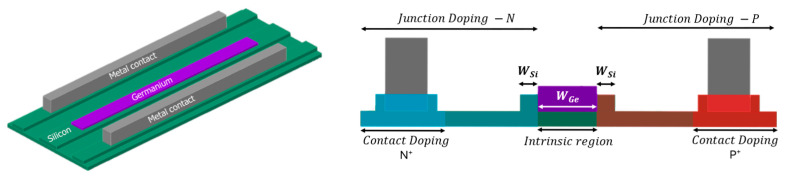 Figure 1
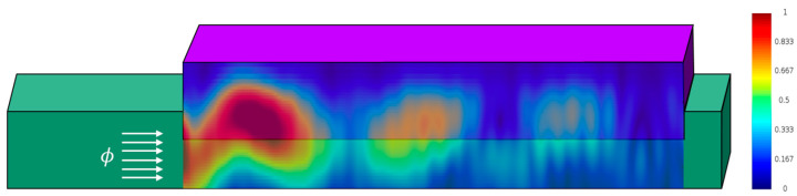 Figure 2
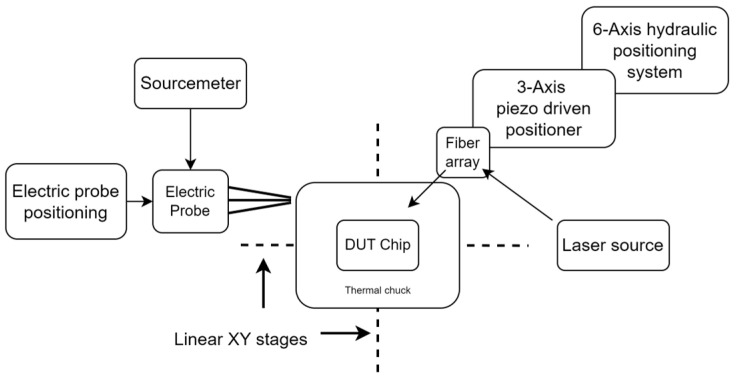 Figure 3
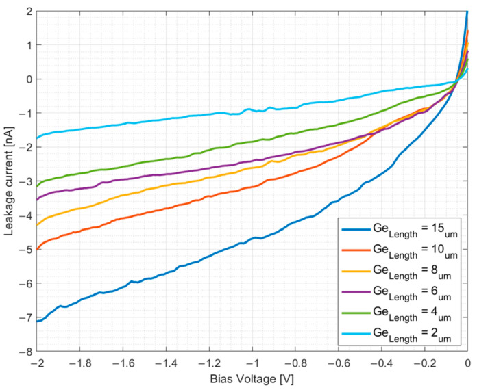 Figure 4
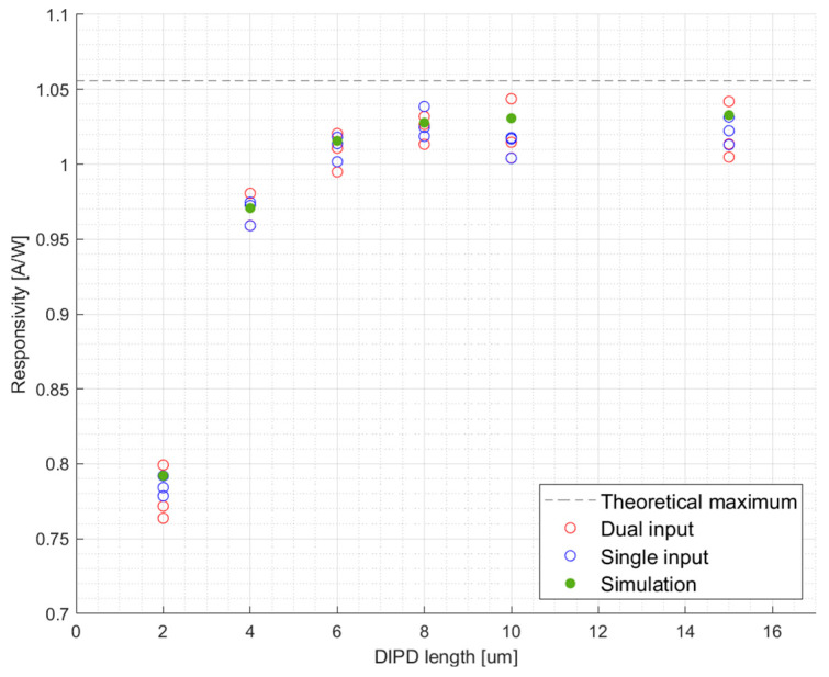 Figure 5
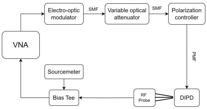 Figure 6
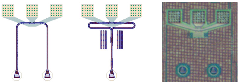 Figure 7
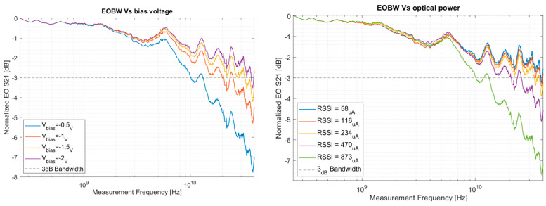 Figure 8
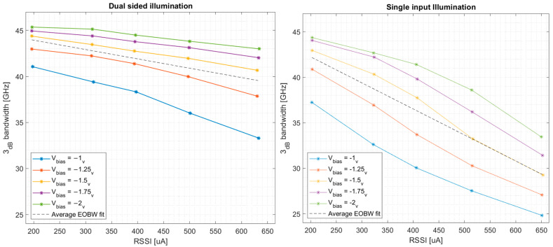 Figure 9
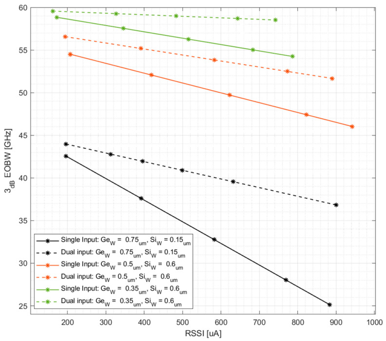 Figure 10
Peer Reviews
No public reviews on file for this paper yet. If you reviewed it on a platform where reviews are public (OpenReview, ICLR, NeurIPS, ICML), you can paste yours below so the community can read it here.
Videos
No videos yet. Explain this paper in a talk, walkthrough, or lecture? Add one.
Taxonomy
TopicsPhotonic and Optical Devices · Advanced Optical Network Technologies · Thin-Film Transistor Technologies
1. Introduction
Silicon photonics has emerged as a promising technology platform for high-speed communications systems [1], particularly in datacenter applications. The ability to manufacture and interconnect photonic and electronic integrated circuits using CMOS-compatible fabrication processes has opened avenues for fast, energy-efficient, and cost-effective optical interconnect over distances and bitrates unattainable with conventional copper interconnects [2]. As industry progresses toward terabit-scale communication, the performance requirements for fundamental electro-optic components such as modulators and photodetectors have intensified. To support higher modulation formats (such as PAM4), photodetectors must operate at increasingly high optical power levels while maintaining or even increasing their EOBW in order to preserve low bit error rates across the optical link [3]. However, scaling traditional silicon photonics photodetectors to high speeds and high powers presents a fundamental physical challenge: the space-charge effect [4], which stems from a combination of high optical power and the classic exponential decay absorption profile of light (often sharp due to the strong absorption coefficient of traditionally employed germanium(, leading to high local densities of photogenerated charge carriers. As the charge carriers begin to drift towards the electrical contacts of the photodiode, they create a self-induced electric field, which opposes the internal drift field, effectively screening it. Consequently, the velocities of charge carriers are drastically reduced, and the EOBW is severely constrained [5].
In this work, we present a dual-pronged approach for mitigating the negative effects of space-charge: by designing the DIPD’s cross-section for a longer 1/e absorption length and the dual-input architecture, we effectively distribute the optical load across the photodetector and reduce otherwise high local concentration of photogenerated charge carriers, maintaining high responsivity and EOBW. While dual-input designs have been previously explored [6,7], our work demonstrates that synergizing this architecture with active cross-sectional absorption optimization yields further EOBW improvements under high power without increasing leakage current or sacrificing responsivity.
2. Design and Geometry
The DIPD structure features a lateral PIN junction in a silicon rib waveguide fabricated on a standard silicon-on-insulator substrate [8], with an absorbing germanium (Ge) layer grown in an etched recess. This approach was chosen for its high performance and CMOS-foundry compatibility: while all-silicon photodetectors based on bulk-defect absorption exist and have been experimentally demonstrated, they suffer from very weak absorption coefficients, requiring non-CMOS-compatible bias voltages [9,10,11] extremely long devices (hundreds of microns) [10], which add parasitic capacitance and have a significant size footprint, or rely on resonant structures for absorption enhancement [9], which require thermal tuning and are spectral bandwidth limited. In contrast, Ge, with a high absorption coefficient at both C- and O-band wavelengths, is available in commercial SiPh platforms, making it a “go-to” choice for photodetector designs. To demonstrate and study the space-charge effect, we simulate and design a Ge-on-Si waveguide-integrated photodiode cross-section based on a commercial foundry’s silicon photonics platform. 3D finite difference time domain (FDTD) simulations were performed using perfectly matched layer (PML) open boundary conditions with a TE polarized mode source. Standard material models (Palik) were utilized for the complex refractive indices of silicon and germanium at the O-band target wavelength of 1310 nm. The baseline geometry was intentionally optimized for strong absorption. The DIPD’s geometry is shown in Figure 1.
Finite differences time domain (FDTD) simulations illustrated in Figure 2 indicate that the baseline DIPD cross-section design with Ge width of W_Ge_ = 0.75 [μm] and silicon rib width of W_Si_ = 0.15 [μm] is expected to achieve close to maximum theoretical responsivity at a length of 10 [μm], with a 1/e absorption length of approximately ≈1.4 [μm].
3. Methods and Results
Measurements were carried out on a temperature-stabilized die-level tester, based on Physik Instrumente’s F712 Fast alignment positioning for coupling light into the chip, utilizing surface grating couplers, optimized for TE polarization. Photocurrent and responsivity measurements were performed via a semiconductor laser (Santec TSL570) and a precision source-measure unit (Keithley 2400), configured as shown in Figure 3.
Leakage current was measured with precision I–V sweeps, and the results are presented in Figure 4.
To validate FDTD simulations, the cutback method was employed, in which DIPDs featuring the same cross-sectional dimensions with increasing lengths were fabricated. Responsivity characterization is based on fitting the measured photocurrent to the following equation:
The responsivity results obtained from three separate dies for both dual and single input illumination schemes are presented in Figure 5.
We observe a strong correspondence between responsivity predictions from FDTD simulations and the measured responsivity values. The observed discrepancies are primarily attributed to manufacturing tolerances.
Using the strong agreement between the simulated absorption profiles and measured responsivities demonstrated in Figure 4, we extract a 1/e absorption length of approximately ≈1.4 [μm], confirming that nearly all optical power is absorbed in the first few microns of the device (L_eff_ ≈ 4 [μm], resulting in a highly localized volume of charge carriers. Using these results and the analytic derivations in Appendix B, we estimate a threshold carrier concentration and photocurrent at which our baseline device transitions to a space-charge limited (SCL) regime. We assume a simplified uniform charge carrier distribution, serving as a lower bound estimation for local carrier density; since the actual absorption profile is exponential, peak densities at the facet of the DIPD are significantly higher. The critical carrier density ( required to screen the internal drift field at a bias voltage of V_bias_ = −2 [V] is given by
We map this threshold carrier density to a threshold photocurrent generated by the active volume of the device V_active_ via carrier transit time using
Substituting the expression for , we calculate the threshold photocurrent:
While this threshold represents a theoretical onset of field screening rather than a total link failure, it indicates that, at standard operating currents of 500~1000 [μA], the DIPD would operate deeply within the space-charge limited regime.
4. Electro-Optic Small Signal RF Characterization
The electro-optic small signal S21 response (EOS21) was measured using the same die-level tester. The measurement setup, illustrated in Figure 6, utilizes a vector network analyzer (VNA, Rohde Schwarz ZNA67) along with a calibrated EO converter with an internal CW laser source (Thorlabs MX70G). Modulated optical output from the modulator was passed through a variable optical attenuator (VOA, Keysight N7762A) and a polarization controller (General Photonics PSY201). The modulated illumination was directed to the DIPD, and the resulting modulated photocurrent was then collected at the VNA’s electrical port via RF probe and bias tee.
RF measurements were carried out via ground–signal–ground (GSG) probing, and the system was de-embedded to the probe tips to isolate the device’s true S21 response, as demonstrated in Figure 7.
Single optical input RF measurements are demonstrated in Figure 8.
In these measurements, we report performance against the generated DC photocurrent (RSSI) rather than external optical power to isolate intrinsic device performance from variable fiber-to-chip coupling losses, directly correlating our measurements to the internal charge density driving the space-charge effect. Consequently, we observe a direct correlation between EOBW and bias voltage and an inverse correlation with average incident illumination power. The positive relationship with bias voltage is anticipated, as the increased bias reduces the transit times of photogenerated charge carriers by stronger electric drift field. The observed decline in EOBW with higher RSSI demonstrates the bandwidth degradation caused by the space-charge effect.
To overcome this limitation, we implemented a design optimization strategy focused on two physical mechanisms: reducing the carrier transit time and lowering the local photocurrent density. First, the transit time was reduced by narrowing , which directly improves EOBW by reducing the carrier drift duration. Second, to prevent high local charge densities, we distributed the optical load using two methods: widening the Si rib to increase the 1/e absorption length and implementing a dual optical input architecture fed by balanced 50:50 optical splitters. These combined techniques effectively distribute photogeneration alongside the device and balance the optical power.
To validate this approach, optimized DIPD cross-sections featuring reduced Ge widths ( ), increased Si rib width ( ) and an increased Ge length for compensation of the expected absorption reduction were fabricated along with a copy of the baseline design.
In order to better analyze measurement results, we plot the EOBW vs. RSSI for our baseline design in Figure 9.
For methodical comparison between the relative performance of different DIPD designs, EOBW is averaged at each RSSI point over all bias voltages, and the resulting data points are fitted to a linear curve. With a single curve representing the performance merit of each DIPD design, we are now able to present all designs collectively in a single plot, demonstrated in Figure 10. Thus, while Figure 9 demonstrates the performance of a single DIPD cross-section, Figure 10 compares the performance across designs.
For the reader’s reference, Table 1 presents a comparative overview of this work alongside related devices, incorporating reported performance metrics from recent years. It is worth noting that, while metrics such as noise equivalent power (NEP) and specific detectivity ( ) are standard for evaluating free-space and imaging photodetectors, they are fundamentally less applicable to waveguide-integrated datacom photodiodes, as in PAM4 datacenter links; the system is not limited by the absolute minimum detectable signal at the noise floor but rather by bandwidth degradation and saturation under high-power illumination. Furthermore, normalizing performance by physical area (as in ) loses its physical relevance when light is confined within a single-mode guided volume rather than captured from a free-space aperture. Consequently, the standard figures of merit in this domain and the focus of our comparative analysis are responsivity, electro-optic bandwidth (EOBW), and dark current evaluated against specific received signal strength indicator (RSSI) levels, as these directly dictate the optical link budget and high-power operational limits.
5. Summary, Conclusions, and Future Work
This paper presents the design, fabrication and characterization of a high-speed, dual-input waveguide-integrated photodiode (DIPD) tailored for high-power optical communication systems in datacenters.
Experimental results demonstrate that the device achieves a high responsivity of 0.91 [A/W] and a large EOBW of while maintaining a low dark current of at −1.5 V bias. A comprehensive comparison with state-of-the-art devices is provided in the Figure of Merit table in Appendix A. Significantly, this work provides a clear experimental identification of the space-charge effect and demonstrates a successful mitigation strategy. By optimizing the cross-sectional geometry to distribute absorption and utilizing a dual-input architecture for optical load balancing, the DIPD effectively overcomes carrier screening limitations to enable high-speed operation at elevated optical powers.
While this work focused on optimizations for lateral cross-sectional dimensions ( and ), future generations of high-power waveguide photodiodes could benefit from additional co-optimization of the vertical along with the horizontal layer parameters. Specifically, employing a thinner germanium layer could further distribute absorption along the propagation axis, delaying the onset of the space-charge effect. However, this degree of freedom must be carefully co-designed with the lateral waveguide dimensions to prevent the optical mode from delocalizing into the surrounding silicon waveguide. Excessive delocalization would severely reduce the optical confinement factor within the active region, effectively decoupling the light from the germanium and completely halting absorption. Therefore, striking the right balance across all three dimensions through careful co-design will be the key to unlocking the next tier of power handling in terabit-scale optical links.
The reference list from the paper itself. Each links out to its DOI / PubMed record.
- 1NVIDIA GTC March 2025 Keynote with NVIDIA CEO Jensen Huang 2025 Available online: https://www.youtube.com/watch?v=_wa Pv Ow L 9Z 8(accessed on 19 March 2026)
- 2Shekhar S. Bogaerts W. Chrostowski L. Bowers J.E. Hochberg M. Soref R. Shastri B.J. Roadmapping the next Generation of Silicon Photonics Nat. Commun.20241575110.1038/s 41467-024-44750-038272873 PMC 10811194 · doi ↗ · pubmed ↗
- 3Szczerba K. Westbergh P. Karout J. Gustavsson J.S. HaglundÅ. Karlsson M. Andrekson P.A. Agrell E. Larsson A. 4-PAM for High-Speed Short-Range Optical Communications J. Opt. Commun. Netw.2012488510.1364/JOCN.4.000885 · doi ↗
- 4Williams K.J. Esman R.D. Dagenais M. Effects of High Space-Charge Fields on the Response of Microwave Photodetectors IEEE Photon. Technol. Lett.1994663964110.1109/68.285565 · doi ↗
- 5Zimmermann H. Silicon Optoelectronic Integrated Circuits 2nd ed.Springer Berlin/Heidelberg, Germany 2019978-3-030-05822-7
- 6Zhao X. Ma Z. Zhao S. Liang H. Tang G. Zhang Y. Wang J. Side-Coupled High-Power and High-Speed Ge-on-Si Photodetectors Using Lateral Subwavelength Grating Waveguides ACS Photonics 2025126052606210.1021/acsphotonics.5c 01501 · doi ↗
- 7Yan T. Li L. Hao J. Meng J. Zhang B. Zhang Y. Large Bandwidth and High Power Germanium/Silicon Photodetector: A Novel Solution for 100 Gb s–1 Microwave Photonic Links ACS Photonics 2025126662667010.1021/acsphotonics.5c 01684 · doi ↗
- 8Virot L. Benedikovic D. Szelag B. Alonso-Ramos C. Karakus B. Hartmann J.-M. Le Roux X. Crozat P. Cassan E. Marris-Morini D. Integrated Waveguide PIN Photodiodes Exploiting Lateral Si/Ge/Si Heterojunction Opt. Express 2017251948710.1364/OE.25.01948729041142 · doi ↗ · pubmed ↗