Freeform Mode-Engineered Metasurfaces
Zhongjun Jiang, Tianxiang Dai, Shuwei Guo, Soyaib H. Sohag, Yixuan Shao, Chenkai Mao, Andrea Alù, Jonathan A. Fan, You Zhou

TL;DR
This paper introduces a new inverse design framework for creating nanophotonic structures with tailored optical properties for advanced applications.
Contribution
A novel inverse design framework for freeform mode engineering in nanophotonic metasurfaces.
Findings
The framework enables optimization of Mie-type modes in dielectric nanophotonic structures.
Freeform nonlocal metasurfaces with bound states in the continuum are demonstrated.
Applications in sensing, nonlinear optics, and quantum information processing are highlighted.
Abstract
Nanophotonic technologies inherently rely on tailoring light–matter interactions through the excitation and interference of deeply confined optical resonances. However, existing concepts in optical mode engineering remain heuristic and are challenging to extend toward complex and multifunctional resonant phenomena. We introduce an inverse design framework that optimizes near-field distributions, ideally suited to tailoring Mie-type modes within dielectric nanophotonic structures, and we demonstrate its application to the discovery of new classes of nonlocal metasurfaces. We show that freeform nonlocal metasurfaces supporting accidental bound states in the continuum can be readily optimized for tailored illumination conditions, modal properties, and quality factors. We further generalize the framework to higher-order and multifunctional mode engineering and experimentally demonstrate…
Genes, proteins, chemicals, diseases, species, mutations and cell lines named across the full text — each resolved to its canonical identifier and authoritative record.
Click any figure to enlarge with its caption.
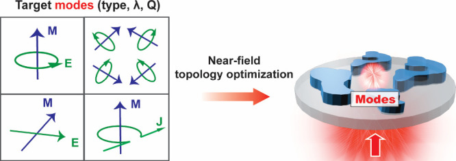 Figure 1
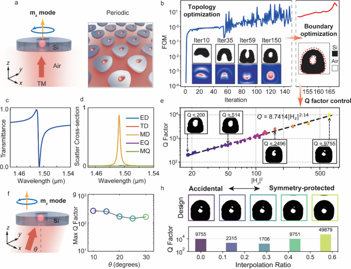 Figure 2
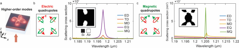 Figure 3
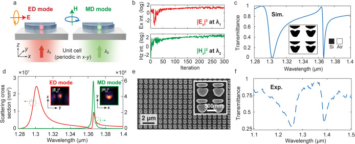 Figure 4
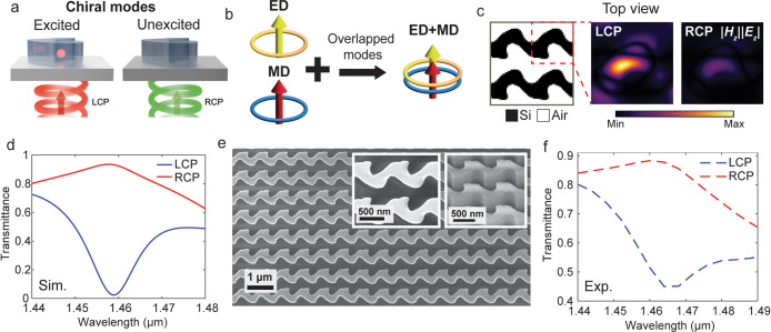 Figure 5
 Figure 6
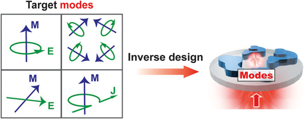 Figure 7
- —National Science Foundation10.13039/100000001
- —Division of Electrical, Communications and Cyber Systems10.13039/100000148
- —Air Force Office of Scientific Research10.13039/100000181
- —Simons Foundation10.13039/100000893
- —Samsung10.13039/100004358
- —University of North Carolina at Charlotte10.13039/100010942
Peer Reviews
No public reviews on file for this paper yet. If you reviewed it on a platform where reviews are public (OpenReview, ICLR, NeurIPS, ICML), you can paste yours below so the community can read it here.
Videos
No videos yet. Explain this paper in a talk, walkthrough, or lecture? Add one.
Taxonomy
TopicsMetamaterials and Metasurfaces Applications · Plasmonic and Surface Plasmon Research · Acoustic Wave Phenomena Research
Light–matter interactions bridging free-space waves and nanoscale resonant modes are crucial in the quest to engineer near- and far-field optical responses in nanophotonic technologies. Modal descriptions of photonic media provide a basis for delineating and engineering near-field hotspots essential for enhancing molecular sensing, ?−? ? fluorescence emission, ?−? ? ? and optical nonlinearities. ?−? ? ? In the far field, designed optical antennas with customized modes support tailored scattering profiles and can collectively function as optical phased arrays. ?,? Using the more general framework of Mie resonance engineering, the tailored excitation, coupling, and interference of electric and magnetic multipolar resonances serve as the basis for the Kerker effect? and tailored bianisotropy, ?−? ? ? which are utilized in Huygens’ metasurfaces, ?−? ? optical cloaks, ?−? ? and large-angle metagratings. ?,?−? ? Recent research efforts have applied these ideas to engineered nonlocalities, based on guided mode resonances and quasi-bound states in the continuum (BIC), ?,? which can be tailored to enable far-field spectral filtering ?−? ? and wavefront engineering with narrow band responses. ?−? ? ?
Despite the important role of resonances in this quest, a pathway to rationally tailor customized optical modes in structured media remains elusive due to the lack of precise analytical correlations between nanoscale geometry and near-field distributions. This observation is emblematic in the typical design process of nonlocal metasurfaces,? which consists of a combination of physical intuition combined with numerical experiments. In a typical workflow, nanostructure geometries featuring nonradiating optical modes are proposed and identified using known physical relationships between nanostructures and modal symmetries. The layout symmetry is then carefully broken with spatially tailored perturbations to enable weak coupling pathways between these highly confined modes and free-space radiation. Full-wave simulation sweeps are critical to empirically relating symmetry breaking with nonlocal responses and building an alphabet of perturbations that allows the spatial structuring of nonlocal modes.? These approaches have been highly effective at developing the foundation of nonlocal metasurface research. ?,?,?−? ? However, the complexity of local mode engineering and nonlocal responses that can be realized with these methods is limited, and it is challenging to extend these concepts to nonintuitive geometric shapes that support full customization of multiple modes and functionalities within a single metasurface platform. It is not even clear whether there are fundamental limits to how many modal responses and functionalities can be packed within a single ultrathin metasurface. In addition, the role of symmetries in the initial design makes it easier to tackle radiation toward high-symmetry points, and sophisticated dispersion engineering needs to be explored to rationally design metasurfaces with lower symmetry radiation.?
In the following, we introduce a computational framework for freeform optimization of Mie-resonant metasurfaces, based on adjoint optimization, ?,? which enables the explicit design of customized optical modes in the near-field. While inverse design techniques have been widely used to shape the far-field wavefront responses of metasurfaces, ?,?−? ? ? ? ? the design of physical nanostructures that support customized modal responses has remained underexplored. Our approach bridges nanoscale mode engineering with freeform topology optimization, enabling the optimization of high-quality-factor (Q-factor) metasurfaces within an exceptionally large design space and facilitating the discovery of new classes of nonlocal metasurfaces with a complex nanophotonic response. The workflow of our computational approach is presented in Figure. Given a desired near-field or far-field metasurface response, we first build a framework of the desired optical mode physics (Figure, left) and specify the mode profile, orientation, Q-factor, wavelength, and complex amplitude. To tailor the coupling between free-space waves and the desired nanoscale modes, we utilize an adjoint variables method (AVM) ?,? adapted to the near-field, in which forward and adjoint simulations utilize a combination of near-field and far-field excitation sources (Figure, right). Our study uses a basic local gradient descent optimizer, though the local gradients calculated using AVM can ultimately be used in conjunction with a wide range of local and global optimization algorithms. ?,?,? For this study, we use far-field signatures as a straightforward, experimentally accessible readout mechanism of the engineered modal states, which relate via coupled mode theory ?,? (Supplementary Section 1).
Our freeform optimization strategy, in which low-performing geometric layouts evolve toward high-Q-factor structures with desired modal profiles, supports distinctive features compared to conventional nonlocal metasurface design approaches. Our platform is ideally suited for full-wave solvers and fully accounts for and exploits the complex relationship between nanoscale freeform shape and optical mode properties without approximations. It does not need to assume or enforce high symmetries pertaining to the photonic nanostructures and incident waves, and it is therefore particularly useful at discovering new classes of accidental BIC structures that are challenging to identify through heuristic designs. Our platform also readily extends to devices hosting multiple multipolar resonances using multiobjective optimization, and it can fully tailor the wavelength, Q-factor, complex amplitude, and spatial position of each mode in the device.
To illustrate the basic concept with a simple model system, we consider the design of a nonlocal, periodic silicon metasurface as a numerical testbed for mode engineering. We select an operating wavelength of 1500 nm with a period of 750 nm along the x- and y-directions, and we tailor the device to couple a normally incident plane wave to an out-of-plane magnetic dipole Mie mode (m _ z _) (Figurea). The m _ z _ mode has been identified in prior quasi-BIC-based metasurface demonstrations as the basis for high-Q metasurface implementation. ?,?,?,?,? To ensure that only this Mie-type mode is supported in the metasurface, the film thickness is limited to 150 nm (≈ λ/10), suppressing higher-order multipolar resonances. Furthermore, the planar metasurface unit cell boundaries are specified to be air to isolate the meta-atom structures from their neighbors, which suppresses the formation of delocalized mode profiles spanning multiple unit cells (see details in Supplementary Section 2).
A figure of merit (FoM) ?,? is defined to maximize the complex amplitude of the desired m _ z _ Mie fields in the metasurface, given the desired incident far-field excitation source. A precise AVM setup for our problem therefore involves the forward source being a normally incident wave and the near-field adjoint source capturing the m _ z _ Mie mode profile. Given the finite spatial extent of the modal profiles, the natural FoM for this problem would be to maximize a spatial overlap integral with the target near-field distributions. ?,? Interestingly, we have found that it is possible to simplify our FoM to the maximization of the complex field amplitude at a point centered within the silicon metasurface unit cell and to use the excitation of a point dipole m _ z _ source when performing adjoint simulations. Our use of a point dipole adjoint source yields a simple and numerically stable FoM and is effective because our nonlocal metasurface system exhibits an enhanced Mie mode optical density of states, and as the photonic Mie mode dielectric structures form during optimization, coupling between the point source and emergent Mie structure leads to predominantly Mie mode-based near-field profiles.
Our optimization algorithm utilizes a two-part AVM-based optimization pipeline (see detailed workflow in Supplementary Section 3). First, density-based topology optimization is performed to identify metasurface topologies that roughly capture the desired coupling between the far-field source and near-field modes. Second, we fine-tune the modal properties and Q-factors using AVM-based boundary optimization. A challenge posed by the optimization of high Q-factor photonic devices is the extreme sensitivity of the device properties to geometric perturbations. To address this challenge, we introduce a neuro-parametrization scheme to describe the metasurface layout, in which a neural network encodes analytic relationships between position and device layout.? Such a scheme circumvents spatial resolution limits posed by density-based AVM design concepts by specifying layout features with unlimited spatial resolution. It also introduces new ways to include constraints important to experimental fabrication, such as feature size and curvature constraints, by framing constraints in the form of loss function engineering during network training and geometry updating.
The optimization trajectory tracking the FoM is presented in Figureb and shows three parts. First, the design is initialized as a uniform grayscale permittivity profile, and a density-based AVM optimization is performed with continuous grayscale dielectric values to identify a promising device topology. Over the course of optimization, the FoM consistently increases and is ultimately enhanced by five-orders-of-magnitude compared to the starting FoM (Figureb, blue line). Second, the device evolves into a binarized freeform structure consisting of Si and air, and the magnetic field distribution within the structured media gradually transforms into a localized hot spot, indicating the emergence of a high-Q magnetic resonance (Figureb, inset). The transmission spectrum of the metasurface after this stage (Figurec) features a narrow-band Fano resonance dip within a broadband transmission window, which is typical of the interference between radiative and nonradiative modes. To confirm the excitation of the m _ z _ Mie mode in the metasurface, we performed a multipolar decomposition of the metasurface near-fields from the current density distributions induced in the nanoscale resonators.? As shown in Figured, the modal decomposition reveals the excitation of a dominant magnetic dipole resonance and no additional noticeable modes. Third, the FoM is fine-tuned using AVM-based boundary optimization with our neuro-parametrization scheme (Figureb, orange line) to further push the Q-factor limit. The detailed tuning of the Q-factor as a function of the out-of-plane magnetic field intensity |H _ z _ | ^2^ is shown in Figuree and shows a linear trend consistent with the relation FE^2^ ∝ Q, where FE denotes the local electromagnetic field. This trend is consistent with those known for critically coupled, lossless single-mode systems.? The insets show the gradual geometric modifications of the high-resolution features, leading to varying Q-factors, with the highest value reaching 10^4^.
The designed meta-atom exhibits an asymmetric “donut” shape that resembles previously studied symmetry-protected designs; ?,?,? however, our structure ultimately utilizes distinct physics. Symmetry-protected BICs require symmetry constraints pertaining to the photonic nanostructures and the incident wave, typically emerge at the center of the Brillouin zone, and are supported in highly symmetric arrays operating under normal incidence. In contrast, our approach facilitates accidental BIC formation purely from structural engineering, ?,? enabling new classes of nonlocal metasurfaces featuring asymmetric geometries and illumination conditions. As a demonstration, we designed a series of accidental BIC metasurfaces for different oblique incidence angles (Figuref). As shown in Figureg, the Q-factors of the optimized metasurfaces may be consistently pushed above high values with minimal shift in the resonance frequency (Supplementary Section 4). To confirm that the freeform-designed BICs are accidental and not symmetry protected, for the device optimized for normal incidence, we perform a shape interpolation between the freeform structure and that of a symmetric donut structure. As shown in Figureh, the corresponding Q-factors decrease during the intermediate stages of shape interpolation and then increase again as the geometry approaches the symmetric layout. This nonmonotonic trend highlights a transition between the accidental and symmetry-protected BIC schemes (see detailed field analyses and additional freeform accidental BIC designs in Supplementary Sections 5 and 6).
Our approach can be generalized to the specification of higher-order Mie modes (Figurea) by defining more complex adjoint sources tailored to the corresponding near-field modal profiles. To demonstrate, we optimize freeform metasurfaces that host clean electric and magnetic quadrupoles, thereby providing a route toward the coupling of far-field radiation to dipole-forbidden processes relevant to nonlinear optics,? surface-enhanced Raman scattering, ?,? and quantum emission enhancement. ?,? A schematic design setup for the electric quadrupole (EQ) mode (Figureb) shows the adjoint sources are implemented by placing four in-plane oriented electric dipoles inside the unit cell, positioned and oriented to match the desired quadrupolar field distribution. ?,? We employ a multiobjective FoM defined as the sum of pointwise field intensities at these four probe locations. The multipolar decomposition (Figureb, right) of the designed metasurface reveals a clean EQ excitation. To the best of our knowledge, such clean quadrupole excitation free of coupled dipolar contents has not been previously demonstrated in the metasurface platform. ?−? ? By switching the adjoining sources to four in-plane magnetic dipoles, the same scheme yields a freeform metasurface supporting a clean magnetic quadrupole (MQ) resonance (Figuresc). We anticipate that our adjoint-source formulation can extend the framework to other complex, nontrivial modes, such as toroidal ?,?,?,? and anapole ?,? resonances, which we leave for future work.
Our computational optimization framework can be readily extended to multifunctional metasurfaces, including the multiplexed excitation of various Mie modes with distinct properties within a single unit cell. As a first demonstration, we design a multiwavelength nonlocal freeform metasurface that supports a pair of dipole resonances, each operating at distinct wavelengths and featuring distinct mode symmetries and resonant properties. The optimization setup is shown in the schematic in Figurea and shows the specification of two Mie-type modes in a periodic meta-array, an in-plane electric dipole (p _ x _) and an out-of-plane magnetic dipole (m _ z _) at the wavelengths of 1.3 and 1.365 μm, respectively. To co-optimize the two target modes, we define a composite FoM within the metasurface as the sum of the ED and MD mode intensities, | E _ x (λ_1)| ^2^ + | H _ z (λ_2)| ^2^. The optimization trajectory of the mode intensities (log scale) at the two target wavelengths is shown in Figureb, indicating a consistent increase in FoM over the course of optimization. The simulated transmission spectrum (Figurec) and multipolar decomposition (Figured) confirm strong electric and magnetic resonances hosted within the metasurface (see more detailed modal analysis in Supplementary Section 7).
We experimentally validate the design by fabricating the optimized metasurface within a 150 nm-thick polycrystalline silicon film on a fused silica substrate. The metasurface patterns are defined using electron beam lithography and reactive ion etching. Figuree presents the top-view scanning electron microscopy (SEM) images of the meta-atoms, showing well-defined geometric features consistent with the design. The measured transmission spectrum (Figuref) confirms the presence of the two target dipole modes with broadened line widths due to slight off-normal incidence of the beam (see Supplementary Section 8).
As a second demonstration, we design a freeform metasurface that utilizes spectrally overlapped multimode resonances to produce planar chiral nonlocal responses, ?,? specifically spin-selective responses that are exclusively induced by circularly polarized light of a specific handedness (Figurea). Single-layer metamaterial systems supporting strong chiroptical responses generally require the electric and magnetic fields to be collinear and spatially overlapped within the dielectric medium.? To achieve these criteria, we use multiobjective optimization to specify spectrally and spatially overlapping E _ z _ and H _ z _ dipole modes that support collinear electric and magnetic field components (Figureb). We specifically define the multivariate FoM to be | E _ z _ || H _ z _ | at a point within the metasurface to promote a balanced ED/MD response, and the FoM is specified to be maximized only when the metasurface is illuminated by left-hand polarized light (LCP) incidence.
The metasurface is designed for a wavelength of 1460 nm and a period of 750 nm. The silicon layer thickness is specified to be 450 nm, and it is relatively thicker compared to prior demonstrations to break the radiation symmetry in the forward and backward directions. A top view of the optimized chiral metasurface is shown in Figurec (left), and the corresponding near-field |E _ z _|| H _ z _ | distributions under LCP (Figurec, middle) and RCP (Figurec, right) illumination show strongly selective Mie mode excitations. The simulated transmission spectra under LCP and RCP illumination, measured by the total transmitted power (Figured), show a 94% circular dichroism (CD) response at the design wavelength (see additional modal and CP-conversion analyses in Supplementary Sections 9 and 10).
We experimentally validate the design by patterning and etching a 450 nm-thick silicon film on a fused silica substrate, and the top-view SEM image of the fabricated device is shown in Figuree. The left inset provides a close-up view of the nanoscale features, revealing well-defined curvilinear geometries with smooth, vertical sidewalls. The measured transmission spectra for the two CP illuminations (Figuref) show spectral line shapes that match well with the simulation. We attribute the reduced CD and broadened line width in the experimental device to fabrication imperfections and the slight off-normal incidence of the laser beam (see Supplementary Section 11). Further enhancements can be achieved by imposing more stringent feature size constraints to mitigate sensitivity to fabrication imperfections. ?,?−? ?
In summary, in this work, we have introduced and demonstrated a near-field inverse design framework to realize freeform resonant metasurfaces through the explicit engineering of optical modes. Our approach accounts for and exploits the complex interplay between nanoscale freeform shapes and optical near-fields, which enables full customization of optical modes in both spatial and spectral domains through efficient exploration of the freeform design space. We anticipate many future extensions of this work. One is the extension of our concepts beyond single-layer media to multilayer ?−? ? ? ? and aperiodic? nonlocal metasurfaces, which can lead to qualitatively new regimes of mode multiplexing capabilities. Another involves incorporating spatial perturbations into engineered nonlocality to achieve spatial and momentum light control. ?,? One other opportunity explores the utilization of faster electromagnetic solvers and optimizers, ?,? which may address current computational bottlenecks in throughput and speed. On the application front, we anticipate that our ability to customize optical near-fields has the potential to impact many application domains including molecular sensing, where conventional nonlocal metasurfaces are limited due to the location of hotspots within the metasurface nanostructures and where our platform can be used to define customized hotspots in near-field regions outside of the metasurface nanostructures. Multifunctional hotspot engineering also has applications in nonlinear optics, ?,? optomechanics, ?,? and quantum emission enhancement? and photochemistry, ?,? where strong and tailored light–matter interactions are required.
Supplementary Material
The reference list from the paper itself. Each links out to its DOI / PubMed record.
- 1Tittl A.Imaging-based molecular barcoding with pixelated dielectric metasurfaces Science 201836019791105110910.1126/science.aas 976829880685 · doi ↗ · pubmed ↗
- 2Khan S. A.Optical Sensing by Metamaterials and Metasurfaces: From Physics to Biomolecule Detection Adv. Opt Mater.202210220050010.1002/adom.202200500 · doi ↗
- 3Wang X.Advances in information processing and biological imaging using flat optics Nature Reviews Electrical Engineering 2024139141110.1038/s 44287-024-00057-2 · doi ↗
- 4Noda S.Fujita M.Asano T.Spontaneous-emission control by photonic crystals and nanocavities Nat. Photonics 2007144945810.1038/nphoton.2007.141 · doi ↗
- 5Pelton M.Modified spontaneous emission in nanophotonic structures Nat. Photonics 2015942743510.1038/nphoton.2015.103 · doi ↗
- 6Russell K. J.Liu T.-L.Cui S.Hu E. L.Large spontaneous emission enhancement in plasmonic nanocavities Nat. Photonics 2012645946210.1038/nphoton.2012.112 · doi ↗
- 7Khoram E.Yu Z.Hassani Gangaraj S. A.Adjoint-Optimized Large Dielectric Metasurface for Enhanced Purcell Factor and Directional Photon Emission ACS Omega 20249243562436110.1021/acsomega.3c 1036238882077 PMC 11170643 · doi ↗ · pubmed ↗
- 8Koshelev K.Subwavelength dielectric resonators for nonlinear nanophotonics Science 2020367197928829210.1126/science.aaz 398531949078 · doi ↗ · pubmed ↗