Improving Fabrication and Performance of Porous Silicon Electron Emission Devices via Functional Layer Resistivity Modulation
Jinxin Dong, Xiaojing Huyan, Fangzhou Luo, Guanyang Zhang, Qiang Liu, Yawen Li, Tianbao Hu, Yongxun Liu, Shinan Wang, Wenjie Yu

TL;DR
Researchers improved the fabrication and performance of porous silicon electron emission devices by using an epitaxial silicon film to control resistivity, leading to better uniformity and stable electron emission.
Contribution
A new method using epitaxial silicon films and ion implantation to modulate resistivity and enhance device fabrication and performance.
Findings
Using an epitaxial silicon film enabled resistivity modulation and improved etching uniformity in porous silicon devices.
Devices achieved a maximum electron emission current density of 80 μA/cm² with high stability.
Electron emission current density remained stable for 4 hours of continuous operation under DC mode.
Abstract
To improve the process controllability and fabrication uniformity of porous silicon (PS)-based electron emission devices (EEDs), we employed an epitaxial (epi) silicon film as the functional layer, leveraging its advantages of high crystalline quality and flexibility of resistivity modulation regardless of the substrate. Precise modulation of the epi film resistivity was achieved via ion implantation. We investigated the effects of resistivity modulation on the fabrication process and device performance. This scheme enabled the formation of PS through electrochemical etching without illumination, and therefore etch self-termination. As a direct result, the etching uniformity in both the vertical and horizontal directions is enhanced. It then facilitated the optimization of the oxidation of the PS surface, which is essential for EED performance. The devices exhibited a maximum electron…
Genes, proteins, chemicals, diseases, species, mutations and cell lines named across the full text — each resolved to its canonical identifier and authoritative record.
Click any figure to enlarge with its caption.
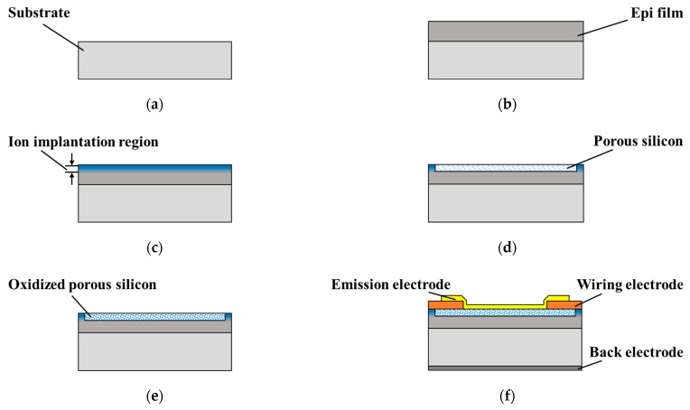 Figure 1
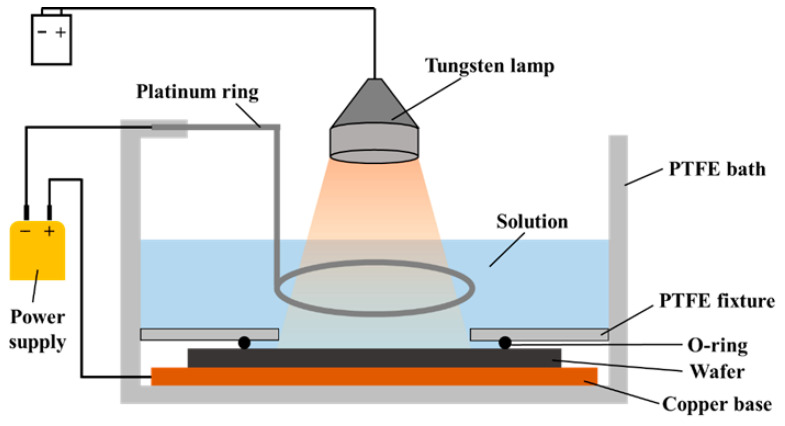 Figure 2
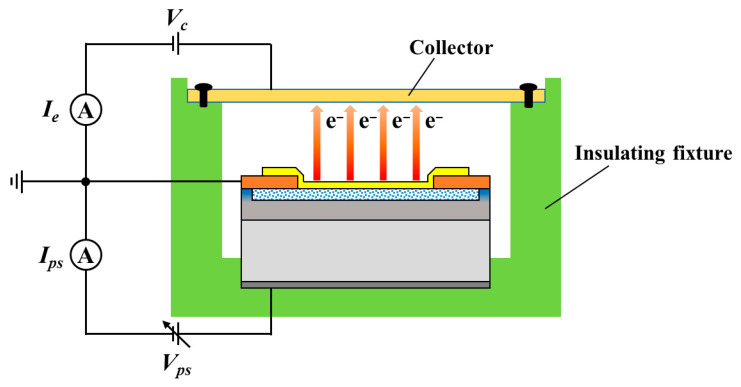 Figure 3
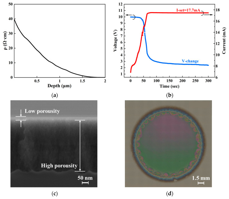 Figure 4
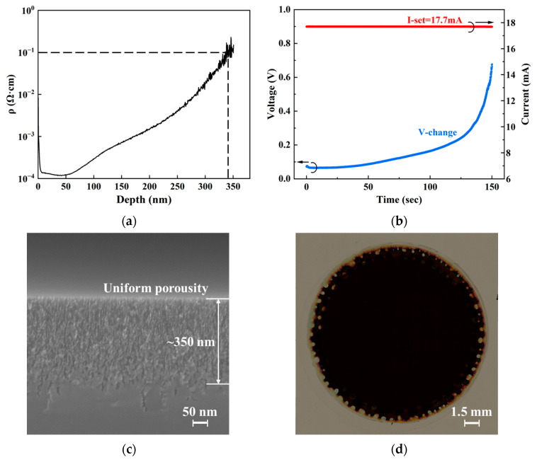 Figure 5
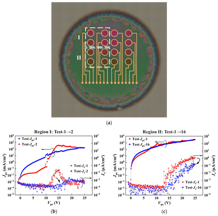 Figure 6
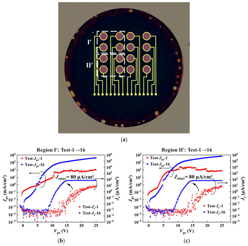 Figure 7
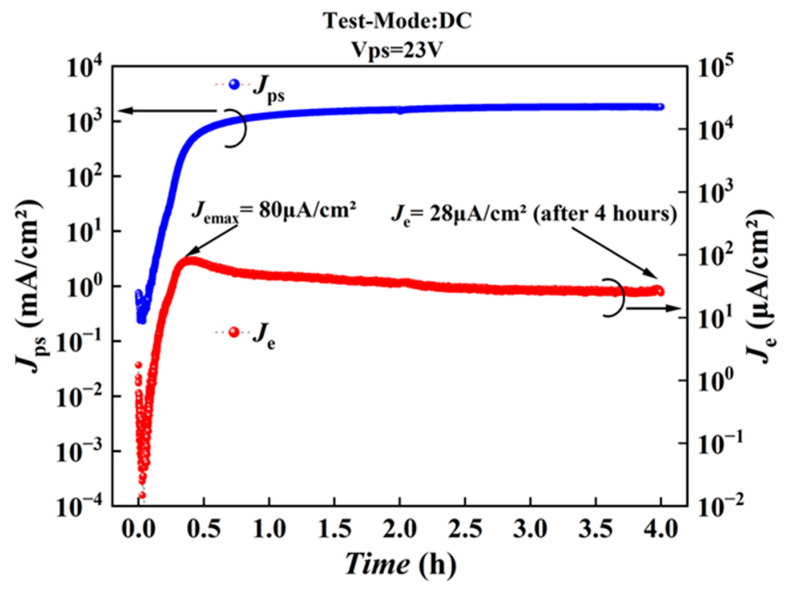 Figure 8
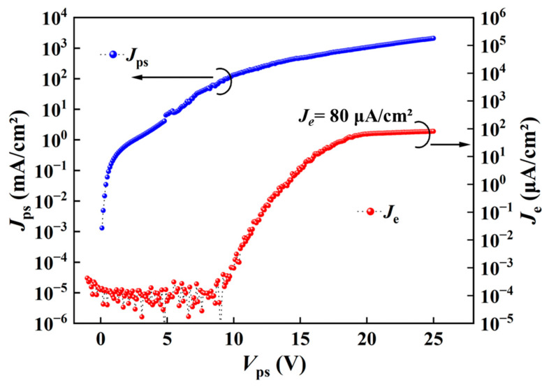 Figure 9
Peer Reviews
No public reviews on file for this paper yet. If you reviewed it on a platform where reviews are public (OpenReview, ICLR, NeurIPS, ICML), you can paste yours below so the community can read it here.
Videos
No videos yet. Explain this paper in a talk, walkthrough, or lecture? Add one.
Taxonomy
TopicsSilicon Nanostructures and Photoluminescence · Silicon and Solar Cell Technologies · Nanowire Synthesis and Applications