Negative Schottky Barriers and Spin-Polarized Fermi Crossings at WSe2/NbSe2 Interfaces
Oliver J. Clark, Anugrah Azhar, Thi-Hai-Yen Vu, Benjamin A. Chambers, Federico Mazzola, Sadhana Sridhar, Geetha Balakrishnan, Aaron Bostwick, Chris Jozwiak, Eli Rotenberg, Sarah L. Harmer, Mohammad Saeed Bahramy, Michael S. Fuhrer, Mark T. Edmonds

TL;DR
This paper explores how the interface between WSe2 and NbSe2 creates spin-polarized Fermi crossings, offering insights for spintronic devices and next-gen transistors.
Contribution
The study reveals a negative Schottky barrier and tunable spin-polarized Fermi crossings at the WSe2/NbSe2 interface.
Findings
A negative Schottky barrier height of ~−30 meV is observed at the WSe2/NbSe2 interface.
Spin-polarized charge carriers form a surface-localized Fermi surface at the K-point valleys.
Increasing WSe2 thickness shifts Fermi pockets from K to Γ, enabling tunable semimetallic phases.
Abstract
Discovering and engineering spin-polarized surface states in the electronic structures of condensed matter systems is a crucial first step in the development of spintronic devices, wherein spin-polarized bands crossing the Fermi level can facilitate information transfer. Here, through nanofocused angle-resolved photoemission spectroscopy (nano-ARPES) and density functional theory-based calculations, we show that the interface between monolayer WSe2 and metallic NbSe2 exhibits a negative Schottky barrier height of ∼ −30 meV: the K-point valleys of the semiconducting layer are shifted by ∼800 meV to produce a surface-localized Fermi surface populated only by spin-polarized charge carriers. By increasing the WSe2 thickness, the Fermi pockets can be moved from K to Γ, demonstrating tunability of novel semimetallic phases that exist atop a substrate additionally possessing charge density…
Genes, proteins, chemicals, diseases, species, mutations and cell lines named across the full text — each resolved to its canonical identifier and authoritative record.
Click any figure to enlarge with its caption.
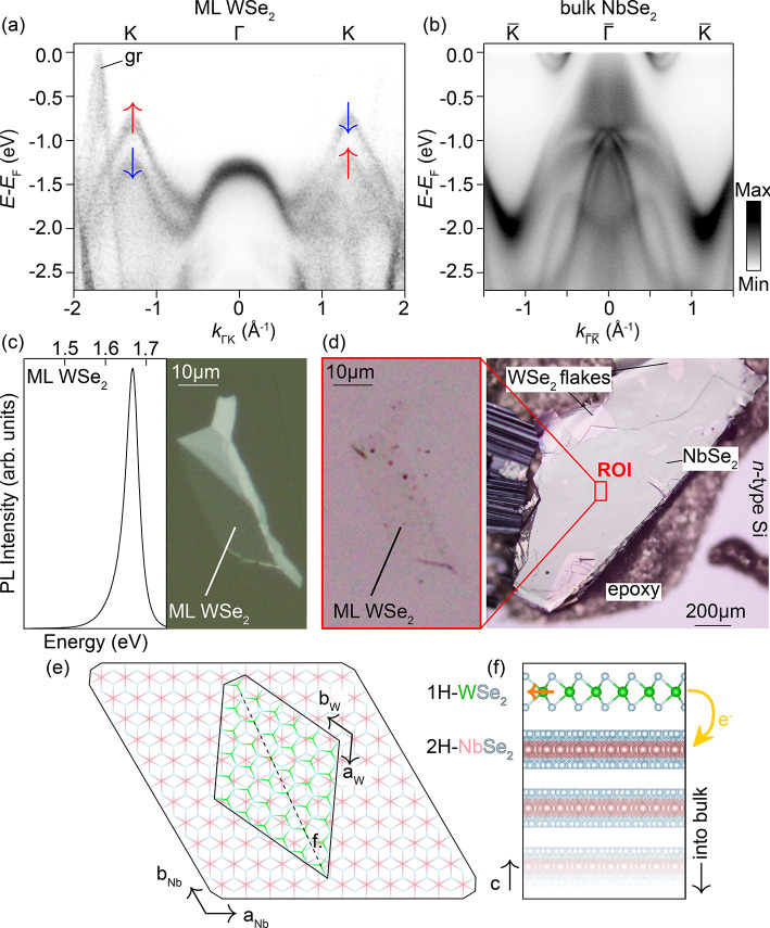 Figure 1
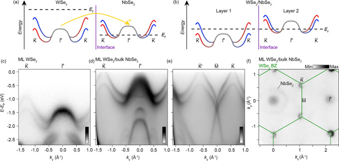 Figure 2
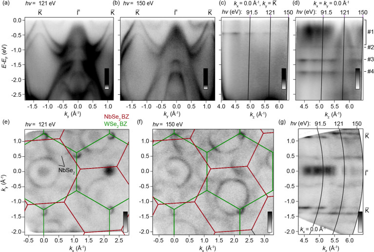 Figure 3
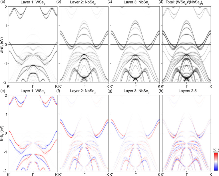 Figure 4
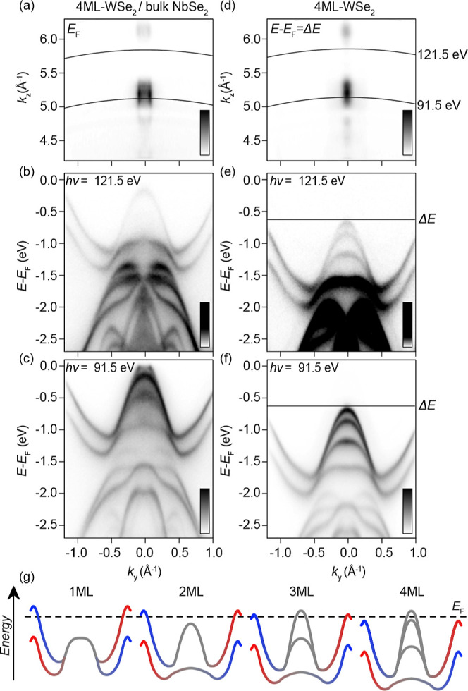 Figure 5
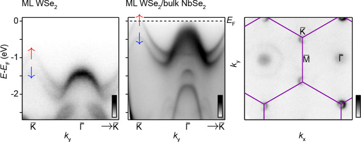 Figure 6
 Figure 7
 Figure 8
 Figure 9
 Figure 10
 Figure 11
Peer Reviews
No public reviews on file for this paper yet. If you reviewed it on a platform where reviews are public (OpenReview, ICLR, NeurIPS, ICML), you can paste yours below so the community can read it here.
Videos
No videos yet. Explain this paper in a talk, walkthrough, or lecture? Add one.
Taxonomy
Topics2D Materials and Applications · Topological Materials and Phenomena · Advanced Thermoelectric Materials and Devices