Triggering avalanche-like ultraviolet photomultiplication phenomena in ultrathin amorphous/crystalline gallium nitride heterostructures
Dongyang Luo, Haochen Zhang, Yong Yan, Wei Chen, Danhao Wang, Huabin Yu, Xin Liu, Yang Kang, Muhammad Hunain Memon, Zhixiang Gao, Yuanmin Luo, Si Liu, Wengang Gu, Boon S. Ooi, Lan Fu, Sheng Liu, Haiding Sun

TL;DR
Researchers created a new type of photodetector that achieves high light sensitivity with very low background noise using a unique amorphous/crystalline material interface.
Contribution
A novel amorphous/crystalline interface design enables trap-assisted carrier multiplication without impact ionization, reducing dark current.
Findings
The a-GaON/GaN heterostructure achieved a gain of 3.9 × 10⁶ and responsivity of 4.3 × 10⁷ A/W at 35 V.
Dark current was as low as ~0.7 pA, outperforming state-of-the-art UV avalanche photodiodes.
The device was integrated into proof-of-concept UV hardware systems for optoelectronic applications.
Abstract
Avalanche phenomena, triggered by carrier multiplication through impact ionization under high electric fields, form the operating principle of avalanche photodiodes. However, this process inevitably leads to amplified dark current, thereby limiting the photo-to-dark-current ratio despite large gain. Here, we demonstrate avalanche-like nonlinear photocurrent amplification while we maintain ultralow dark current in an amorphous-gallium oxynitride (a-GaON)/gallium nitride (GaN) heterostructure formed via a two-step “amorphization-recrystallization” process. Instead of relying on the impact ionization process, the engineered amorphous/crystalline interface enables trap-assisted photo-induced carrier multiplication behavior at low voltages, yielding a large gain (3.9 × 10⁶) and ultrahigh responsivity (4.3 × 10⁷ amperes per watt) at 35 volts, with an ultralow dark current (~0.7 picoamperes),…
Genes, proteins, chemicals, diseases, species, mutations and cell lines named across the full text — each resolved to its canonical identifier and authoritative record.
Click any figure to enlarge with its caption.
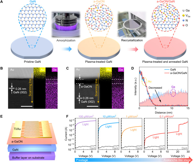 Figure 1
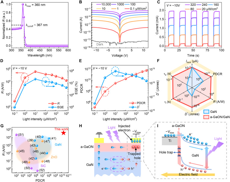 Figure 2
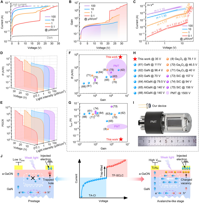 Figure 3
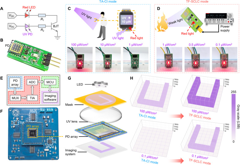 Figure 4
Peer Reviews
No public reviews on file for this paper yet. If you reviewed it on a platform where reviews are public (OpenReview, ICLR, NeurIPS, ICML), you can paste yours below so the community can read it here.
Videos
No videos yet. Explain this paper in a talk, walkthrough, or lecture? Add one.
Taxonomy
TopicsGaN-based semiconductor devices and materials · Thin-Film Transistor Technologies · Ga2O3 and related materials