Large-scale gate-all-around MoS2 transistor array through lossless monolithic 3D integration
Chao Chen, Kuanglei Chen, Hang Zhao, Shucao Lu, Jinsen Shang, He Jiang, Li Gao, Xiaoyu He, Shihua Jiang, Zhangyi Chen, Zheng Zhang, Xiankun Zhang, Yue Zhang

TL;DR
A new 3D integration process improves the performance of MoS2 transistors by avoiding interface doping issues, making large-scale production feasible.
Contribution
A lossless monolithic 3D integration process is introduced to enable high-performance MoS2 gate-all-around transistors.
Findings
The process achieves an average on-state current density of 227 μA/μm with a peak of >335 μA/μm.
Gate-all-around transistors show a 46% reduction in resistance capacitance delay compared to planar structures.
The interface engineering strategy significantly reduces dielectric doping and improves transistor performance.
Abstract
Integrating 2D materials into 3D architectures can break through the physical limits of materials in advanced processes. However, challenges such as severe interfacial doping caused by dielectric deposition during vertical stacking processing have led to performance degradation in MoS2 3D gate-all-around (GAA) field-effect transistors (FETs), thereby severely hindering their large-scale integration. Here, we demonstrate a lossless monolithic 3D (M3D) integration process flow enabled by using an interface engineering strategy to achieve the highly uniform large-scale integration of multichannel MoS2 GAAFETs with ultrahigh current density. This strategy involves reducing interface states and dielectric doping by forming van der Waals contacts with MoS2 and creating hydrophilic surfaces for high-κ dielectric deposition via an Sb2O3 layer, thereby significantly improving the performance of…
Genes, proteins, chemicals, diseases, species, mutations and cell lines named across the full text — each resolved to its canonical identifier and authoritative record.
Click any figure to enlarge with its caption.
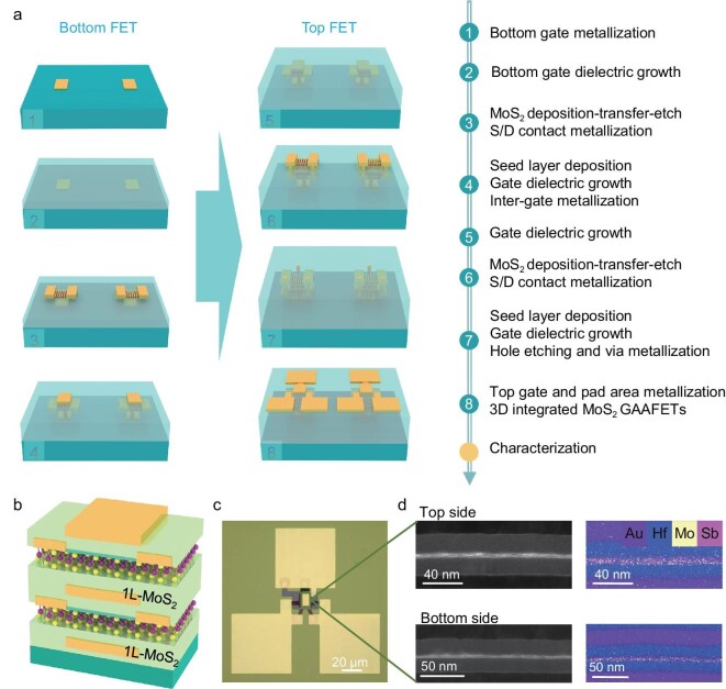 Figure 1
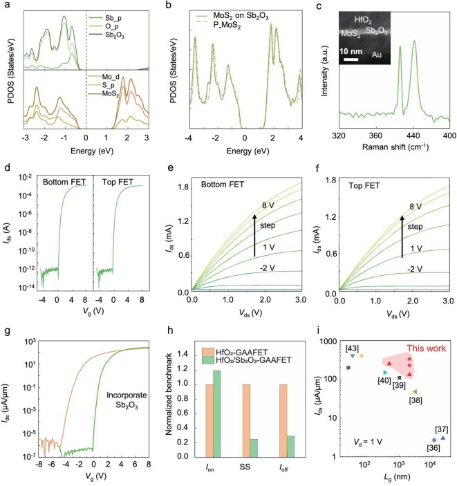 Figure 2
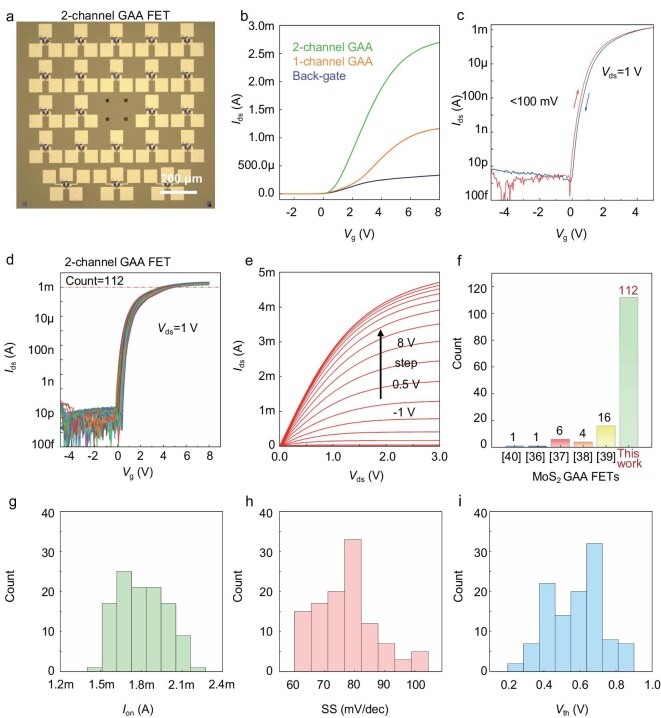 Figure 3
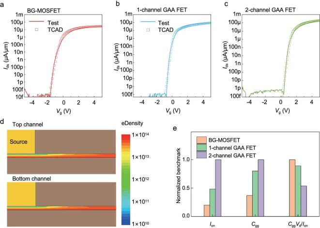 Figure 4
Peer Reviews
No public reviews on file for this paper yet. If you reviewed it on a platform where reviews are public (OpenReview, ICLR, NeurIPS, ICML), you can paste yours below so the community can read it here.
Videos
No videos yet. Explain this paper in a talk, walkthrough, or lecture? Add one.
Taxonomy
Topics2D Materials and Applications · Nanowire Synthesis and Applications · Thin-Film Transistor Technologies