Investigation of III-Nitride MEMS Pressure Sensor for High-Temperature Applications
Makhluk Hossain Prio, Maruf Morshed, Lavanya Muthusamy, Md Sohanur E. Hijrat Raju, Itmenon Towfeeq, Durga Gajula, Goutam Koley

TL;DR
This paper explores a high-temperature MEMS pressure sensor using AlGaN/GaN transistors that performs reliably at up to 300 °C.
Contribution
A novel high-temperature MEMS pressure sensor using AlGaN/GaN HEMTs with stable performance and tunable sensitivity is presented.
Findings
The sensor showed a 0.65% resistance change at 250 °C under 35 kPa pressure.
Theoretical simulations matched experimental results closely at room temperature.
The sensor operated stably up to 300 °C with a response time under 10 ms.
Abstract
High-temperature operation of AlGaN/GaN Heterojunction Field Effect Transistor embedded diaphragm-based MEMS pressure sensors have been investigated, which utilized their wide bandgap and piezo resistivity to perform stably at elevated temperatures. The performance of the pressure sensor was observed over a change in applied pressure of 35 kPa, which resulted in an experimentally measured change in drain–source resistance (ΔRDS/RDS(0)) of 0.32% at room temperature and 0.65% at 250 °C, respectively. Additionally, the COMSOL-based Finite Element (FE) Simulations, in conjunction with our developed theoretical model, was utilized to theoretically determine the change in drain–source resistance. This theoretically calculated ΔRDS/RDS(0) of 0.45% at room temperature closely aligns with the experimental observations. Moreover, the sensor exhibited a gate-bias-dependent tunability, with the…
Genes, proteins, chemicals, diseases, species, mutations and cell lines named across the full text — each resolved to its canonical identifier and authoritative record.
Click any figure to enlarge with its caption.
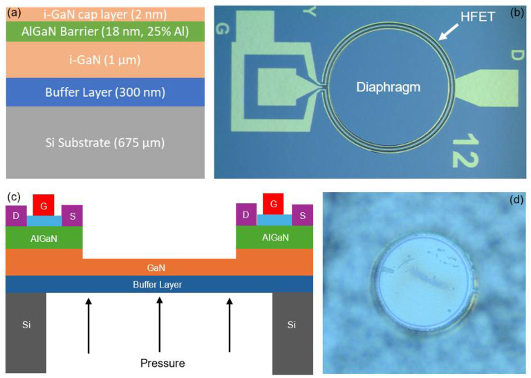 Figure 1
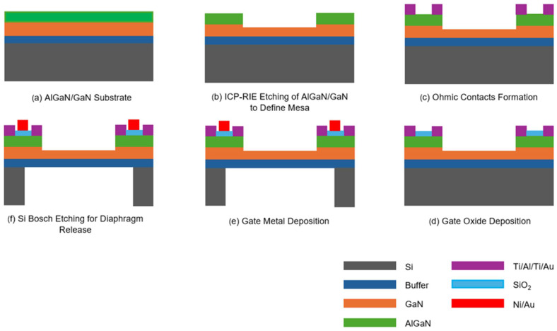 Figure 2
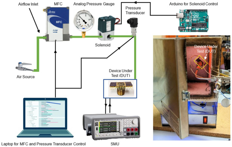 Figure 3
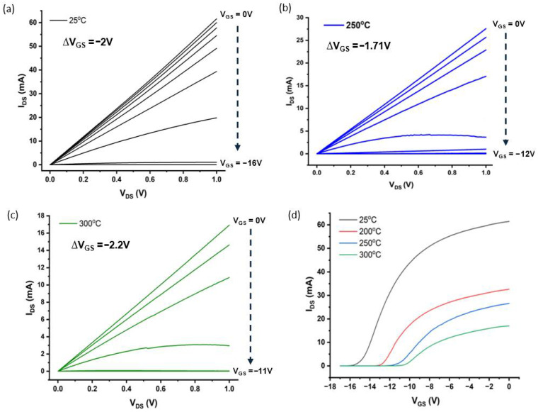 Figure 4
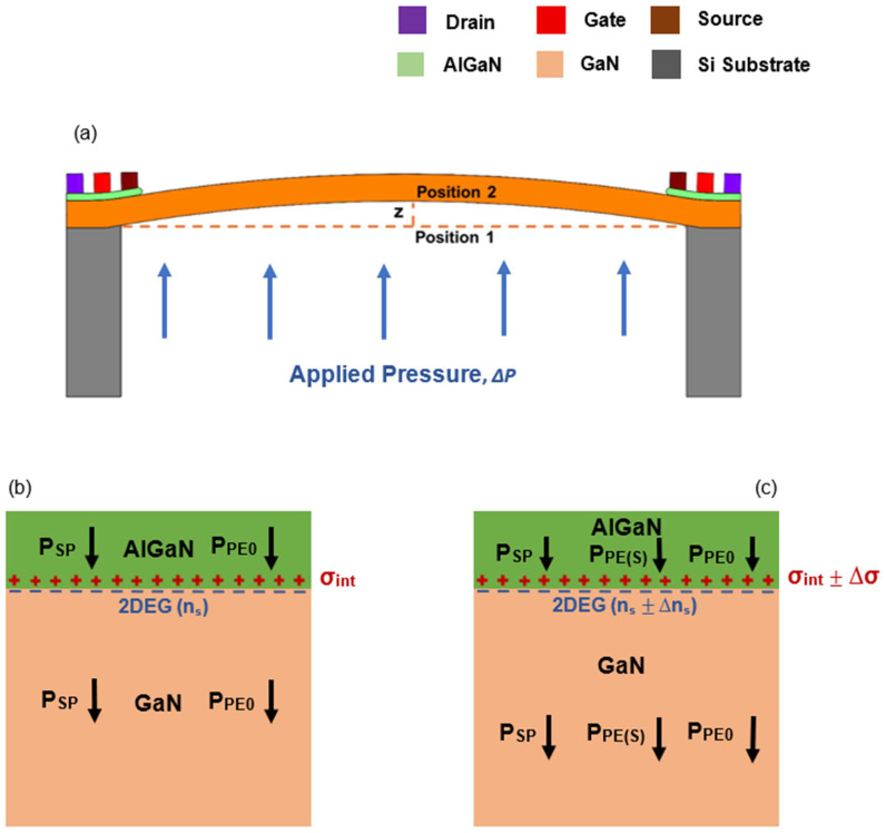 Figure 5
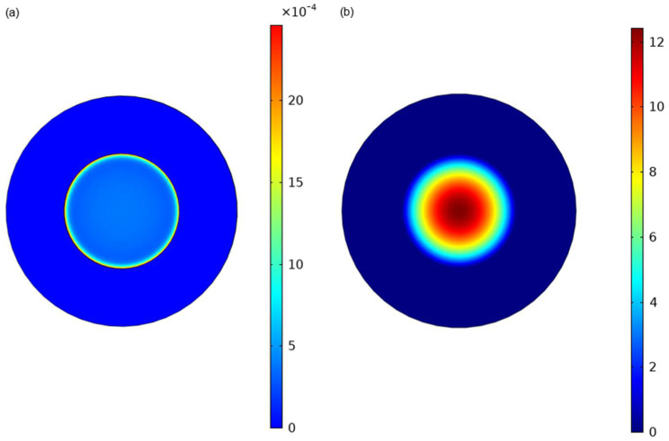 Figure 6
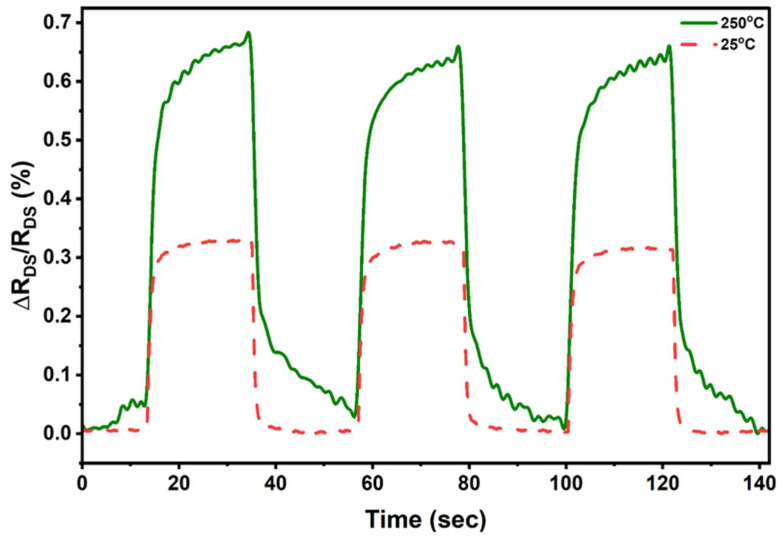 Figure 7
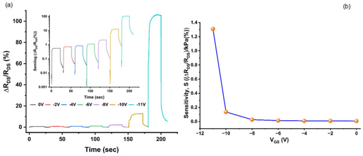 Figure 8
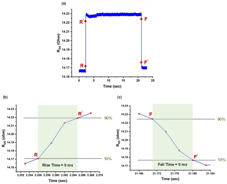 Figure 9
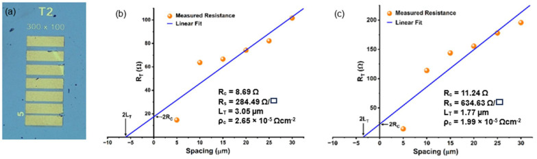 Figure 10
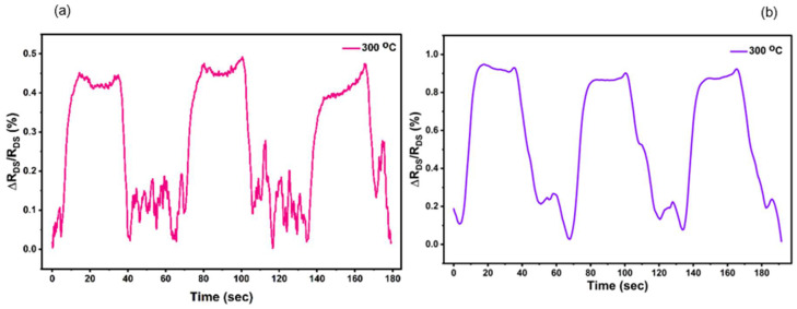 Figure 11
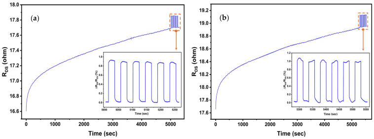 Figure 12
- —National Science Foundation
Peer Reviews
No public reviews on file for this paper yet. If you reviewed it on a platform where reviews are public (OpenReview, ICLR, NeurIPS, ICML), you can paste yours below so the community can read it here.
Videos
No videos yet. Explain this paper in a talk, walkthrough, or lecture? Add one.
Taxonomy
TopicsAdvanced MEMS and NEMS Technologies · Advanced Sensor and Energy Harvesting Materials · Magnetic Field Sensors Techniques
1. Introduction
Pressure sensors operate by transducing applied pressure into measurable electrical outputs, such as changes in resistance, voltage, or capacitance [1,2]. In harsh environments, such as in the aerospace, automotive, oil and gas, deep-well drilling, nuclear power, and petroleum industries, there is a great need for high-temperature-compatible pressure sensors [3,4,5,6,7,8]. At present, piezoresistive [9], capacitive [10], piezoelectric [11], and triboelectric [12] pressure sensors have been utilized for high-temperature applications [1,2,13,14]. Additionally, fiber optic sensors demonstrate thermal stability in extreme and flammable environments for oil and gas downhole applications due to their characteristics of using optical fiber as the sensing medium [5,6,8].
Recent advancements in microelectromechanical systems (MEMS) technology have enabled substantial progress in the design of pressure sensors and actuators incorporating MEMS-based sensing elements. Applications in sectors such as oil and gas, automotive, defense, aerospace/avionics, and nuclear power increasingly demand MEMS devices capable of reliable operation under harsh environmental conditions, including elevated temperatures, high humidity, mechanical shock and vibration, overload stress, radiation exposure, and corrosive chemical environments [15]. In addition to miniaturization, MEMS pressure sensors offer several key advantages: low power consumption, high sensitivity, reduced mass and volume, precise measurement capabilities in confined spaces, low manufacturing cost, minimal disturbance to the measured system, compatibility with monolithic integration of sensing and processing electronics, and suitability for large-scale batch fabrication [2,15,16].
Owing to the narrow bandgap of silicon (~1.12 eV) [17], conventional silicon-based MEMS are typically limited to operating temperatures below ~125 °C [18], and their performance deteriorates significantly above ~150 °C due to the generation of thermal carriers and high leakage currents [4], which makes it less suitable for harsh environments. Silicon also suffers from insufficient corrosion resistance at elevated temperatures, further constraining its use under prolonged extreme conditions [4]. Therefore, scientists have explored solutions for alternative materials and transduction mechanisms capable of maintaining stable operation in such environments [8,15].
Among these, III-Nitride-based MEMS technologies have garnered particular attention. For example, P. Leclaire demonstrated AlN-based MEMS devices [19]. In recent years, AlGaN/GaN HEMT-based MEMS received special interest [4]. It is chemically inert, mechanically stable, and radiation hardened, which makes it a promising device material for hostile environments. The strong polarization fields at the AlGaN/GaN heterointerface induce a two-dimensional electron gas (2DEG) [4], which is strongly responsive to strain. AlGaN/GaN MEMS-based pressure sensors exhibit high sensitivity since both the 2DEG density and the mobility can be modulated with the strain, while only the carrier mobility gets modulated with the applied strain in silicon, providing comparatively lower values for sensitivity. These characteristics of the AlGaN/GaN interface make them better a better-suited material for sensing applications over silicon [4,8,16,20]. Numerous studies have demonstrated the pronounced strain sensitivity of the 2DEG in AlGaN/GaN heterostructures [21,22,23,24,25,26], enabling its effective use for pressure transduction [27,28,29,30]. Additionally, the wide bandgap of GaN (3.4 eV) facilitates stable device performance at elevated temperatures, positioning AlGaN/GaN HEMT-based MEMS as strong candidates for high-temperature sensing applications [8].
AlGaN/GaN heterostructures are commonly realized using metal–organic vapor phase epitaxy (MOVPE) [31], hydride vapor phase epitaxy (HVPE) [32], and molecular beam epitaxy (MBE) [33] growth techniques, with MOVPE offering a key advantage in providing highly uniform, scalable, and device-quality AlGaN/GaN layers suitable for large-area wafers and industrial fabrication. AlGaN/GaN heterostructures grown by atmospheric-pressure MOVPE on GaN demonstrate that epitaxial quality is governed by precursor chemistry and strain management [31]. Increasing Al incorporation via higher trimethylaluminum (TMA) flow reduces the growth rate and degrades crystalline quality due to parasitic reactions and strain relaxation, whereas lowering the trimethylgallium (TMG) flow enhances Al incorporation while improving structural and optical properties, enabling higher Al-content growth [31]. In contrast, lower Al composition AlGaN layers exhibit superior crystalline quality and suppressed crack formation due to minimized lattice mismatch with GaN, making them particularly favorable for high-quality heterostructures and device applications [31].
Another relevant technology for high-temperature pressure sensors is the piezoresistive Si-on-insulator (SOI), which consists of layers of silicon, silicon dioxide, and silicon, as well as other relevant materials. Using Smart-Cut™ processing, SOI pressure sensors with an active silicon layer as thin as 340 nm have demonstrated operation at temperatures approaching 600 °C [34]. For SOI-type pressure sensors, despite their potential for being operated at higher temperatures, the Si material is susceptible to creep at elevated temperatures, leading to its diminished sensitivity and stability. These limitations restrict their applicability in various high-temperature applications, such as aerospace, automotive, and deep-well drilling [17]. Another technique to sense pressure is capacitive-based, which measures changes in pressure due to changes in the distance between electrodes [35]. High-temperature implementations of capacitive sensors have been realized using alumina (Al_2_O_3_) [36] and silicon carbide (SiC) [37] platforms [8]. However, the motion of the capacitive sensor is constrained to small vertical and horizontal movements [38]. If the vertical displacement is large, the capacitance is not suitable for pressure sensing [4]. Given these constraints, research attention has increasingly shifted toward diaphragm-based GaN pressure sensors. In these systems, diaphragm motion—and thus pressure sensitivity—is governed primarily by the material’s intrinsic yield strength rather than by geometric limitations [4]. Coupled with GaN’s high theoretical temperature tolerance, which may reach up to ~600 °C [4,39], AlGaN/GaN-based diaphragm sensors offer a compelling path forward for robust, high-temperature pressure sensing. Additionally, oxidation of III-Nitride films below 500 °C is minimal, as demonstrated by Suria et al. [40].
Additionally, Silicon Carbide’s (SiC) wider bandgap enables their MEMS pressure sensors to be operated at elevated temperatures. Silicon carbide-based piezo resistive pressure sensors at temperatures of up to 600 °C have been studied [41,42,43]; however, these devices demonstrated low output signals and low-pressure sensitivity values [4]. Furthermore, Chen et al. reviewed advances in various types (piezoresistive, capacitive, piezoelectric, fiberoptic, and friction electric) of high-temperature pressure sensors based on inorganic materials (such as silicon, silicon carbide, sapphire, and ceramics) and high-temperature resistant polymers, with detailed analysis on material properties, sensing mechanisms, and temperature compensation methods [1].
Advantages of GaN over SiC include higher mobilities (especially for GaN heterostructures), higher critical break down fields, lower on-resistances, and higher switching speeds [8]. Despite their considerable potential, GaN-based microelectromechanical systems (MEMS) experienced slow technological maturation for many years, largely due to the challenges associated with fabricating III-nitride epilayers on substrates such as SiC and sapphire, which are difficult to etch. Recent advances in the epitaxial growth of high-quality III-nitride films on Si (111) substrates have significantly mitigated these limitations, enabling rapid expansion of III-nitride MEMS research and development. As a result, a wide range of III-nitride–based MEMS devices—including RF filters, pressure sensors, acoustic sensors, and microcantilevers—has now been successfully demonstrated [44].
There have been various studies on AlGaN/GaN-based pressure sensors for room-temperature sensing applications [28,45]. In this work, we have investigated the pressure-sensing characteristics of our AlGaN/GaN Heterojunction Field Effect Transistor (HFET) integrated diaphragm pressure sensor across temperatures ranging from room temperature to 300 °C. We determined the change in drain–source resistance and sensitivity, both experimentally and theoretically, caused by a change in applied pressure. The theoretical values were calculated using COMSOL 6.0-based FE simulations, coupled with a theoretical model. The devices demonstrate stable operation up to 300 °C, underscoring their promise for high-temperature harsh environment applications.
2. Materials and Methods
The pressure transducers investigated in this study were fabricated on AlGaN/GaN epitaxial layers deposited on (111) silicon wafers, procured from NTT Advanced Technology Corporation, Tokyo, Japan. The wafer structure comprised a 2 nm i-GaN cap layer and an 18 nm Al_0.25_Ga_0.75_N layer atop a 1 µm i-GaN layer, with a 300 nm buffer layer separating the GaN layer from the silicon substrate, which measured 675 µm in thickness. The fabrication process began with etching the uppermost 100 nm of the AlGaN/GaN layer using BCl_3_/Cl_2_ plasma chemistry to define the mesa region around the diaphragm periphery. Subsequently, a metal stack consisting of Ti (20 nm)/Al (100 nm)/Ti (45 nm)/Au (55 nm) was deposited, followed by rapid thermal annealing at 825 °C for one minute to establish ohmic contacts for the source and drain regions of the HFET. Next, a 100 nm layer of SiO_2_ was deposited over the exposed mesa regions using the plasma-enhanced chemical vapor deposition (PECVD) method, serving as the gate dielectric. This step was followed by two sequential metallization stages. The first stage involved depositing a Ni (25 nm)/Au (200 nm) stack as gate metal contacts, and the second stage deposited a Ti (20 nm)/Au (225 nm) stack to form the probe contacts. Finally, the Bosch process was used from the bottom face of the sample to perform through wafer etching of silicon to release the diaphragm. Figure 1a shows the layer structure of the fabricated pressure-sensing device and Figure 1b presents the optical microscopic image of the pressure sensor to reveal its physical structure, with HFET in its periphery connected to the contact pads. The diaphragm has a nominal radius of 500 µm, while the width of the drain, gate, and source is 10 µm each. Moreover, Figure 2 depicts the diagrammatic representation of process flow for the fabrication of pressure sensors.
Controlled air pressures of P1 and P2 (P1 + ∆P, where ∆P is the change in applied pressure) were maintained at regular intervals utilizing a mass flow controller (MFC) operated through a LabView program and a solenoid valve (Model Name: SMC VT307-5GI-02, SMC Corporation of America, Noblesville, IN, USA), managed by an Arduino Uno R3 microcontroller. To monitor the pressure, an analog pressure gauge (Model Name: WIKA 0–30 in Hg Vacuum/160 PSI, F.N. Cuthbert, Inc., Toledo, OH, USA) was integrated into the air tube line. Additionally, a digital pressure transducer (Model Name: DATAQ 2000361/-HS, DATAQ Instruments, Inc., Akron, OH, USA) was installed, alongside the analog gauge to provide enhanced accuracy in pressure measurements. For testing and characterization, the pressure sensor chip was mounted on a ceramic chip carrier, and the metal contact pads were wire-bonded to the external leads of the carrier. The device was biased at the drain–source terminal using a source measurement unit (Model Name: B2902A Precision Source/Measure Unit, Keysight, Inc., Santa Rosa, CA, USA). For high-temperature testing, the sensor was placed inside a furnace (Model Name: Rapidfire Standard Pro-L, Tabletop Furnace Company, Inc., Lake Katrine, NY, USA) capable of reaching a temperature of 1200 °C. The high-temperature tests up to 300 °C were performed using the tabletop furnace with a ramp rate of 75 °C/min (determined manually). A schematic of the experimental setup is illustrated in Figure 3, showing the MFC, source measurement unit (SMU), pressure gauge, Arduino, and device under test.
3. Results and Discussions
3.1. Temperature-Dependent I-V Characteristics
A dual-channel source measure unit (SMU) (Keysight B2912A) was used to characterize the I–V characteristics of the HFET of the device (Device 1) at both room (25 °C) and higher temperatures (200 °C, 250 °C, and 300 °C). In the I_DS_-V_DS_ measurements (see Figure 4a–c), the drain–source current, I_DS_, was measured by varying the drain–source voltage (V_DS_) from 0 to 1 V, at different constant gate voltages, V_GS_. In the I_DS_-V_GS_ measurements (see Figure 4d), while supplying a constant V_DS_ of 1 V, changes in I_DS_ due to sweeping the V_GS_ were measured. the I_DS_-V_GS_ curves of AlGaN/GaN HFETs with varying temperatures and constant V_DS_ = 1 V are shown in Figure 4d. A good gate control was observed, as the device shut down at both room and higher temperatures, as presented in Figure 4d. The figure also shows that the absolute value of the gate shutdown voltage decreased (shifted to the right) with the increase in temperature, as the gate shutdown voltage values of −16 V, −13.5 V, −12 V, and −11 V were recorded at 25 °C, 200 °C, 250 °C, and 300 °C, respectively. Additionally, the I_DS_-V_DS_ curves (Figure 4a–c) reveal a reduction in I_DS_ for each constant V_GS_, as the temperature increased. This decline can be attributed to the decreased carrier mobility, coupled with the reduction in piezo coefficients, at elevated temperatures [46].
3.2. Theoretical Modeling for 2DEG Formation and Relationship with Strain
To comprehend the operation of AlGaN/GaN heterostructure-based piezotransistive HFET diaphragms, this section will introduce a theoretical model and elucidate how mechanical deflection of the diaphragm under applied pressure induces variations in the HFET channel resistance.
In the absence of external mechanical strain, the bound polarization sheet charge (σ_int_) at the AlGaN/GaN heterostructure interface leads to the formation of a quantum well at the AlGaN/GaN interface, and a two-dimensional electron gas (2DEG) is generated within the well without the need for intentional doping [47,48,49,50,51,52]. Assuming change neutrality through the heterosystem, 2DEG sheet charge concentration at the interfaces is expressed as [51]:
where q is the electron charge, ε0 is the permittivity of free space, ε(x) is the relative dielectric constant of AlGaN, d is the thickness of the AlGaN layer, φ_b_ is the Schottky barrier height, E_F_ is the Fermi level at the heterointerface with respect to the GaN conduction band edge, and ΔE_c_ is the conduction band offset at the AlGaN/GaN interface. Fermi energy can be calculated using effective electron mass, m_eff_ = 0.22m_e_ (where m_e_ is the electron mass) and reduced Planck’s constant (ħ) as E_F_(x) = E0(x)+ n_s_(x), where the ground sub-band level of the 2DEG is given by E0(x) = [ ]^2/3^ [47].
The piezoelectric properties of the AlGaN/GaN heterojunction have been employed to convert diaphragm deflection into an electrical signal in our proposed AlGaN/GaN HFET-embedded diaphragm-based MEMS pressure sensors. This transduction mechanism is illustrated in Figure 5 using a simplified schematic of the diaphragm and the corresponding AlGaN and GaN layers. Figure 5a depicts a schematic of a diaphragm-based AlGaN/GaN pressure-sensing device featuring an HFET located at the diaphragm’s periphery. In the absence of external strain (or pressure), the diaphragm positioned at Position 1 (as shown in Figure 5a) and the corresponding interface charge density (σ_int_) can be expressed in terms of spontaneous polarization (PSP) and piezoelectric polarization (P_PE_) as:
Figure 5b illustrates the σ_int_ and corresponding 2DEG density at the AlGaN/GaN interface without external strain.
When the diaphragm is subjected to change in pressure, it deflects to Position 2 (as shown in Figure 5a) by ensuring the displacement from Position 1. External mechanical strain is induced in both the AlGaN and GaN layers, generating additional piezoelectric polarization, denoted as P_PE_(S)AlGaN and P_PE_(S)GaN, respectively (shown in Figure 5c), due to the difference in their piezoelectric coefficients. This additional strain induced polarization (Δσ) modifies the 2DEG sheet carrier concentration by Δn_s_. Δσ can be given by the difference in the strain-induced (caused by pressure change) piezoelectric polarization at the interface as [53]:
where x represents the Al alloy composition in AlGaN, e31 and e33 are the piezoelectric constants, and ε_x_, ε_y_, and ε_z_ are the average (over the dimensions of the HFET channel) x-, y-, and z-direction strains at the interface due to deflection or bending.
For our proposed pressure sensor, the associated change in 2DEG sheet carrier concentration (Δn_s_) at the AlGaN/GaN heterostructure interface due to Δσ can be given as (considering negligible changes in , E_F_(x), and ∆ (x)) [53]:
where q is the electronic charge, is the permittivity of air, ε(x) is the dielectric constant of Al_0.25_Ga_0.75_N, q is the Schottky barrier height of the gate contact, E_F_(x) is the Fermi energy level, and ∆P_PE_(bending)(x) is the piezoelectric polarization occurring due to diaphragm bending or displacement.
This change in the sheet carrier concentration (Δn_s_), or the conducting channel carrier density of the HFET, changes the drain–source resistance (R_DS_) of the HFET. By maintaining a constant drain–source voltage (V_DS_), the change in R_DS_ (ΔR_DS_) can be observed as a corresponding change in the drain–source current (ΔI_DS_). Conversely, by maintaining a constant drain–source current (I_DS_), the change in R_DS_ (ΔR_DS_) can be observed as a corresponding change in the drain–source voltage (ΔV_DS_). This constant drain–source current (I_DS_) biasing approach is employed in many practical applications, such as ion-sensitive field effect transistors (ISFETs) [54,55,56] and microcantilever resonance amplitude measurements [57], to compensate for biased point shifts. Hence, any deflection of the diaphragm is transduced into a change in electrical signal (ΔV_DS_ or ∆I_DS_) when a constant I_DS_ or V_DS_ is maintained, enabling pressure sensing through the piezotransistive response of the GaN-based diaphragm structure.
3.3. Sensor Characterization at Room Temperature
Due to the strong piezoresistive nature of the AlGaN/GaN interface, diaphragm deflection under pressure altered the two-dimensional electron gas (2DEG) density, affecting resistance in our experiment. This change in resistance, , can be calculated from the relationship among Gauge Factor (GF), 2DEG density, and 2DEG mobility as [4,53,57]:
Upon simplification, we have:
where ∆µ_n_ is the change in mobility, ∆n_s_ is the change in 2DEG mobility density, R_DS_(0) is the initial resistance, ∆R_DS_ is the change in resistance with average applied strain, and ε_av_. µ_n_ and n_s_ are the mobility and carrier concentrations, respectively.
Additionally, the Sensitivity (S) of the pressure sensor can be determined as [4]:
Figure 6 presents Finite Element (FE) simulations conducted using COMSOL Multiphysics (version 6.0, COMSOL Inc., Stockholm, Sweden). Figure 6a illustrates the strain distribution across the diaphragm and Figure 6b shows the diaphragm’s displacement under an applied pressure of 35 kPa above atmospheric pressure. Based on the simulations, the diaphragm’s maximum displacement was approximately 12.2 µm and the displacement is higher at or near the center of the diaphragm. The maximum strain of 24 × 10^−4^ was observed at the circumference of the diaphragm, while the average strain (ε_av_) over the dimensions of the HFET channel is 17 × 10^−4^, as illustrated in Figure 6a. Consequently, the HFETs were strategically positioned at the diaphragm’s periphery to maximize the polarization-induced conductivity changes, thereby enhancing device sensitivity. Table 1 shows the Young’s Modulus, Poisson’s Ratio, and density of both GaN and AlGaN considered for the simulation. We note that the vibration noise [58] can influence device behavior. Finite-element vibration simulations in [58] show that the resonant response of AlGaN/GaN diaphragms is primarily governed by tensile residual stress and diaphragm geometry (diameter and thickness), which can lead to a transition between plate-like and membrane-like dynamics that is critical for sensor optimization [58]. In contrast, the simulations and experiments in [59] show that GaN devices exhibit stable responses to humidity variations, which cause negligible effects at elevated temperature (e.g., 360 °C) [59]. We would like to mention here that the impacts of vibration noise and humidity can be effectively minimized by employing a Wheatstone bridge configuration using devices located on and off the diaphragm [60]. This would further enhance the device’s suitability for operation in harsh environments, including aerospace and oil and gas applications.
Theoretically, we calculated the values for n_s_ and ∆n_s_ as 1.11 × 10^13^ cm^−2^ and −4.6708 × 10^10^ cm^−2^ using Equations (1) and (4), respectively, for our 18 nm thick Al_0.25_Ga_0.75_N layer. The calculated value for n_s_ is supported by the 2DEG density vs. AlGaN thickness curve in the Supplemental Figure S1. Prior to determining ∆n_s_, ∆P_PE_(bending) was obtained as −5.89 × 10^−9^ cm^−2^ using Equation (3). These values are summarized in Table 2. The fractional change in mobility, due to the change in effective mass, is estimated as Δμ_n_/μ_n_ = 0.025% from our prior report [53]. This Δμ_n_/μ_n_, together with the value of Δn_s_/n_s_, yields ΔR_DS_/R_DS_(0) = 0.445% at room temperature (RT), following Equation (6). This value of ΔR_DS_/R_DS_(0) closely matches the experimentally measured value of ΔR_DS_/R_DS_(0) = 0.32% (see Figure 7) at room temperature for Device 1, while exposed to a change in applied pressure of 35 kPa and keeping a constant drain–source voltage, V_DS_ = 1 V and zero gate voltage. This small mismatch can be attributed to the smaller value in Δn_s_ compared to the theoretically calculated value, which can arise from surface and sub-surface carrier trapping—commonly observed in III-nitrides [61] and other wide-bandgap materials that can reduce the effective Δn_s_ in our experiments, compared to the theoretical estimates. We note here that the ΔR_DS_/R_DS_(0) was obtained with the gate voltage, V_GS_ = 0 V, which can increase very significantly with more negative gate bias, as discussed below.
In our pressure sensors, the sensitivity significantly improves as the gate bias becomes more negative. Figure 8a presents the drain–source resistance changes over time under varying gate voltages for the device 1. At gate biases of −2 V and −8 V, the drain–source resistance (R_DS_) changed by 0.7% and 1.1%, respectively, in response to a change in applied pressure of 80 kPa. In comparison, as the gate voltage approached the threshold, under V_GS_ = −10 V and −11 V, R_DS_ changed by 11% and 105%, respectively, highlighting the enhanced sensitivity under higher negative gate bias. As shown in Figure 8b, the sensitivity rises dramatically from 0.009%/kPa at V_GS_ = −2 V to 1.31%/kPa at V_GS_ = −11 V, representing an approximately 150 times increase. Sensitivity values are calculated using Equation (7). This rise is because the sensitivity S, which is proportional to Δn_s_/n_s_ (see Equation (7)), increases as n_s_ reduces due to the application of a more negative V_GS_ [45]. Incidentally, alongside the increase in sensitivity, the Gauge Factor also increased significantly (150 times) from 4.11 to 617.64, with the increase in negative gate bias from −2 V to −11 V, as determined using Equation (5). High sensitivity and Gauge Factor are particularly desirable in sensors as it simplifies circuit design, reduces the impact of noise, and enhances the resolution of pressure measurements limited by noise [44]. Thus, some of the key advantages of our pressure sensor are its gate bias-related tunability and high deflection sensitivity. Compared with commercial pressure sensor devices, we note that the sensitivity of 1.31%/kPa at higher negative gate bias for our pressure sensor is nearly 90 times higher than the sensors from Omega (Model No: PX409 Series) [62] or PCB Piezoelectronics (Model No: 121A45) [63], which currently have one of the best-performing sensors in the temperature range of <150 °C with a sensitivity of 0.015%/kPa [62,63]. However, more negative gate bias can have the potentially undesirable effect of enhancing charge instability as R_DS_ increases significantly [64].
The response time is a critical parameter for evaluating the performance of a pressure sensor. It is defined as the time taken for a sensor’s output to transition from 10% to 90% of its final value during signal increase, and vice versa, during the signal decay [16]. To determine this parameter for our pressure sensor, the sensor’s response to a change in applied pressure of 35 kPa was recorded, as shown in Figure 9a. Figure 9b shows that upon the introduction of 35 kPa change in applied pressure, the sensor required 9 ms (τ_rise_) to reach 90% of its final response from 10%. The transition from 10% to 90% of the final response occurred between 2.256 s and 2.265 s. Similarly, the sensor demonstrated a recovery (decay) time of only 9 ms (τ_fall_), as illustrated in Figure 9c, which is considered sufficient for most practical applications [19]. Nevertheless, further improvements in response time may be possible by addressing the sampling rate, limited by the Source Measurement Unit (SMU), and reducing the mechanical flow delay in the tube and the chamber [19]. In fact, the measured rise or fall time includes the response time of the solenoid valve used to perform pressure switching, which can be estimated to be a few milliseconds for 35 kPa pressure change, from the manufacturer datasheet [65].
In addition to the measurements at 35 kPa and 80 kPa applied pressure changes, we evaluated sensor performance at two additional applied change in pressures—30 kPa and 60 kPa—at room temperature and zero gate bias conditions to assess the sensor sensitivity over a broader applied pressure range spanning 30–80 kPa. To perform these experiments, a separate device (Device 2) was used for measurements under same V_DS_ = 1 V. The device exhibits a good response of ΔR_DS_/R_DS_(0) = 0.1% and sensitivity = 0.003%/kPa under a 30 kPa change in pressure, which increased to ΔR_DS_/R_DS_(0) = 0.27% and sensitivity = 0.004%/kPa under a 60 kPa applied change in pressure. These results are included in the Supplemental File in Figure S2.
3.4. Sensor Characterization at Elevated Temperatures
The pressure-sensing device (Device 1) was tested at 250 °C under identical biasing conditions (V_DS_ = 1 V, V_GS_ = 0 V). As shown in Figure 7, the device continues to exhibit a stable response at elevated temperatures, with a measured relative resistance change of ΔR_DS_/R_DS_(0) = 0.65% and a corresponding sensitivity of S = 0.018%/kPa (determined using Equation (7) under an applied pressure change of 35 kPa), indicating the intrinsic stability and sensitivity of the device performance at higher temperatures. Notably, when the operating temperature increases from RT to 250 °C, the resistance change increases from 0.32% to 0.65% and the sensitivity increases from 0.009%/kPa to 0.018%/kPa. One of the reasons for this increase is that 2DEG is depleted at elevated temperatures [45], coupled with the increase in sheet resistances. Such a decrease in 2DEG density (n_s_) can result in an increased sensitivity as Δn_s_/n_s_ increases, as can be seen from Equation (7).
To verify that increasing temperatures indeed cause 2DEG density and mobility to change, transmission line measurements (TLMs) were carried out at both RT and 300 °C. The TLM structures consisted of probe pads with a width of 100 μm, separated by varying gap lengths ranging from 5 μm to 30 μm. An optical image for TLM pattern is shown in Figure 10a. The resistance values corresponding to each length of semiconductor were measured and plotted as total resistance (R_T_) vs. spacing (l) for RT and 300 °C, respectively, as shown in Figure 10b,c. After the linear fit of the curves for both RT and 300 °C, the contact resistance (R_C_) is calculated from the y-intercept, while the sheet resistance (R_S_) is calculated from the slope of the straight line for each. The transfer length (L_T_), which signifies the effective length of the contact, can be calculated from the x-intercept. The specific contact resistivity (ρc) was calculated as ρ_c_ = R_C_ L_T_W [20].
The measured parameters for TLM patterns are summarized in Table 3. Notably, the contact resistance increased from 8.69 Ω at RT to 11.24 Ω at 300 °C, while the sheet resistance increased nearly 125%, from 284.49 Ω/□ to 634.53 Ω/□ over the same temperature range. This increase in R_S_ indicates that the higher resistance modulation and enhanced sensitivity observed at elevated temperatures arises from a reduction in 2DEG density, as well as electron mobility. The 2DEG mobility change has been reported to be in the range of 70–80% at elevated temperatures [66], which indicates the rest of the change in sheet resistance can be attributed to the change in 2DEG density.
We also investigated the pressure sensor devices at 300 °C. For this, a separate device (Device 3) was utilized to perform similar pressure-sensing experiments at up to 300 °C. However, Device 3 had a smaller diaphragm radius of 375 µm, compared to the 500 µm radius of Device 1. For Device 3, we tested pressure responses at both constant V_DS_ and constant I_DS_ conditions. Figure 11a exhibits the pulsed pressure (80 kPa) responses for constant V_DS_ = 1 V, where the change in drain–source resistance is 0.43% at 300 °C, which is much smaller compared to the 0.65% observed for Device 1 for 35 kPa pressure pulses at 250 °C. The corresponding sensitivities for Device 3 and Device 1 are 0.005%/kPa and 0.018%/kPa, respectively. The magnitude of the pressure pulse was chosen to be higher for Device 3 to account for the reduced strain at the periphery caused by the lower radius of the diaphragm [8]. Since stress (σ) is proportional to the square of the diaphragm radius (r^2^) [8], we expect the sensitivity of Device 3 to be 1.8 times lower compared to Device 1. However, the experimentally observed sensitivity for Device 3 of 0.005%/kPa was found to be 3.6 times lower compared to Device 1, as discussed above. This variation can be caused by fabrication and material-dependent changes in device behavior.
The pressure sensor performance of Device 3 for constant I_DS_ = 10 mA (V_GS_ = 0 V) corresponding to pressure pulses of 80 kPa, for 300 °C, is shown in Figure 11b. Typically, constant I_DS_ measurements result in more stable sensor response due to the compensation of biasing-related instability [54,55,56,57]. This can be readily seen by comparing the pressure-sensing responses in Figure 11a,b. Clearly, the responses observed in Figure 11b are more stable and less noisy, as expected. Interestingly, the sensitivity is found to be 0.01%/kPa in Figure 11b, which is almost doubled that of the constant voltage case, clearly indicating that constant current-based measurements are preferrable to extracting the best pressure-sensing performance from these devices, especially at higher temperatures, where maintaining device bias stability is critical. Nonetheless, our results from Device 3 clearly underline the potential for the proposed pressure sensors to operate at 300 °C with good stability and reliability.
Furthermore, to test the reliability of devices, especially under the application of a negative gate bias, stress tests were conducted with a gate bias of −5 V applied for over 1.5 h for Device 1. The results are shown in Figure 12. We find that the Device 1 exhibited an increase in drain–source resistance (due to charge trapping related instability), which stayed within ~7%. The pressure-related fractional resistance change (ΔR_DS_/R_DS_(0) = 0.9%) was very stable and consistent (inset of Figure 12a) under 80 kPa pressure changes, yielding a sensitivity of 0.011%/kPa. To assess longer-term reliability, the same experiment was repeated after two weeks at V_GS_ = −5 V (following rigorous testing of various temperatures in between), and the results are shown in Figure 12b. We find the device responses to be very similar, with an initial increase in R_DS_ under negative gate bias, but stable and consistent fractional drain–source resistance, ΔR_DS_/R_DS_(0) = 1%, and sensitivity of 0.012%/kPa, indicating no observable degradation. We would also like to point out that increasing the gate bias to values close to the threshold voltage, i.e., V_GS_ = −11 V, as in Figure 8, can result in very high-pressure sensitivity, but the device response becomes somewhat unstable due to the much higher degree of charge trapping. Such instability can also be reduced through the use of a Wheatstone bridge [60]; however, for practical applications, an optimal bias point may need to be determined to achieve both high sensitivity and adequate signal stability.
4. Conclusions
In summary, we have demonstrated a diaphragm-based AlGaN/GaN HFET-embedded circular membrane pressure transducer, capable of stable and repeatable sensing operation at temperatures of up to 300 °C. The device was characterized under a 35 kPa pressure range, and the experimentally measured resistance change (ΔR_DS_/R_DS_(0)) showed agreement with theoretical predictions, validating the sensor’s design and modeling accuracy. Additionally, the transducer exhibited gate-bias-dependent tunability, with sensitivity from 0.009%/kPa to 1.31%/kPa, as gate voltage changed from −2 V to −11 V. The device performance was compared for constant voltage and constant current mode at 300 °C, with the latter exhibiting a much more stable response, with almost double the sensitivity. Overall, the diaphragm-based sensor, with the integrated AlGaN/GaN HFET-based deflection transducer, was found to be promising for high-temperature and high-pressure measurements with good stability.
The reference list from the paper itself. Each links out to its DOI / PubMed record.
- 1Chen Y. Xu Q. Zhang X. Kuang M. Materials and Sensing Mechanisms for High-Temperature Pressure Sensors: A Review IEEE Sens. J.202323269102692410.1109/JSEN.2023.3323318 · doi ↗
- 2Song P. Ma Z. Ma J. Yang L. Wei J. Zhao Y. Zhang M. Yang F. Wang X. Recent Progress of Miniature MEMS Pressure Sensors Micromachines 2020115610.3390/mi 1101005631906297 PMC 7020044 · doi ↗ · pubmed ↗
- 3Prio M.H. Morshed M. Muthusamy L. Gajula D. Koley G. High Temperature Characterization of III-Nitride Pressure Sensors Proceedings of the 2025 Device Research Conference (DRC)Durham, NC, USA 22–25 June 202512
- 4Gajula D. Jahangir I. Koley G. High Temperature Al Ga N/Ga N Membrane Based Pressure Sensors Micromachines 2018920710.3390/mi 905020730424140 PMC 6187712 · doi ↗ · pubmed ↗
- 5Aref S.H. Zibaii M.I. Latifi H. An improved fiber optic pressure and temperature sensor for downhole application Meas. Sci. Technol.20092003400910.1088/0957-0233/20/3/034009 · doi ↗
- 6Fusiek G. Niewczas P. Mc Donald J.R. Design of a highly accurate optical sensor system for pressure and temperature monitoring in oil wells Proceedings of the 2009 IEEE Instrumentation and Measurement Technology Conference Singapore 5–7 May 2009574578
- 7Qi B. Pickrell G.R. Zhang P. Duan Y. Peng W. Xu J. Huang Z. Deng J. Xiao H. Wang Z. Fiber optic pressure and temperature sensors for oil down hole application Proceedings of the SPIE Fiber Optic Sensor Technology and Applications Prague, Czech Republic 14 February 20024578
- 8Chapin C.A. Miller R.A. Dowling K.M. Chen R. Senesky D.G. In Al N/Ga N high electron mobility micro-pressure sensors for high-temperature environments Sens. Actuators A Phys.201726321622310.1016/j.sna.2017.06.009 · doi ↗