Parasitics-Aware Quantum Transport Simulation of Stacked Si Nanosheet LGAA-nFETs for Sub-2 nm Node RF Applications
Qi Shen, Shuo Zhang, Zhi-Fa Zhang, Wenchao Chen, Zekai Zhou, Sichao Du, Hao Xie, Wen-Yan Yin

TL;DR
This paper introduces a quantum transport simulation framework to study parasitic effects and RF performance in stacked Si nanosheet transistors for sub-2 nm applications.
Contribution
A novel quantum transport modeling framework that integrates parasitic effects for RF performance analysis in sub-2 nm stacked Si nanosheet transistors.
Findings
Optimized device configurations achieved cutoff frequencies exceeding 400 GHz.
Maximum oscillation frequencies approached 1.2 THz with proper design.
Parasitic effects significantly impact high-frequency performance metrics.
Abstract
This work presents a comprehensive quantum transport modeling and simulation framework to evaluate parasitic effects and radio frequency (RF) performance in stacked silicon (Si) nanosheet (NS) lateral gate-all-around (LGAA) nFETs targeting the sub-2 nm technology node. Leveraging the non-equilibrium Green’s function (NEGF) method, the proposed framework integrates detailed modeling of parasitic resistances (Rpara) and capacitances (Cpara) to enable a holistic analysis of both intrinsic and extrinsic figures-of-merit, including transconductance (gm), output conductance (gd), cutoff frequency (fT), and maximum oscillation frequency (fmax). The effects of nanosheet geometry, crystal orientations, and dual-k spacers on high-frequency performance are systematically investigated. The analysis reveals key design trade-offs, with optimized device configurations yielding fT exceeding 400 GHz and…
Genes, proteins, chemicals, diseases, species, mutations and cell lines named across the full text — each resolved to its canonical identifier and authoritative record.
Click any figure to enlarge with its caption.
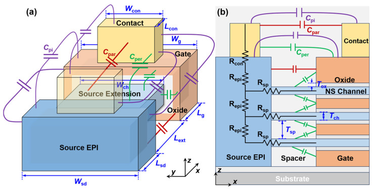 Figure 1
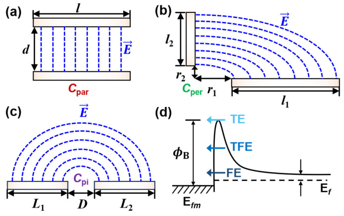 Figure 2
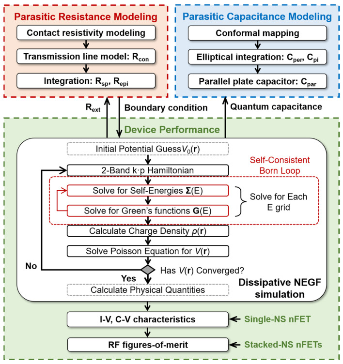 Figure 3
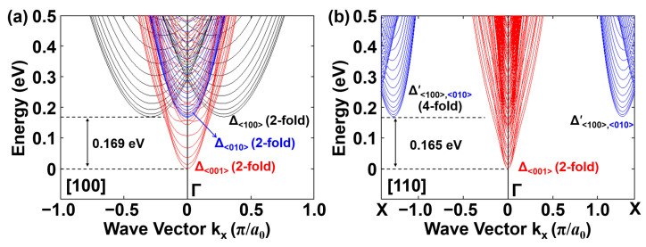 Figure 4
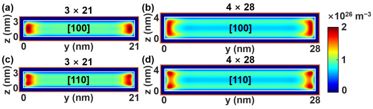 Figure 5
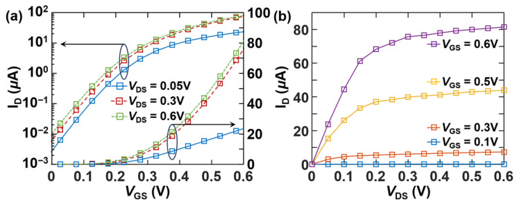 Figure 6
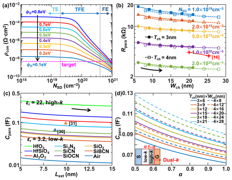 Figure 7
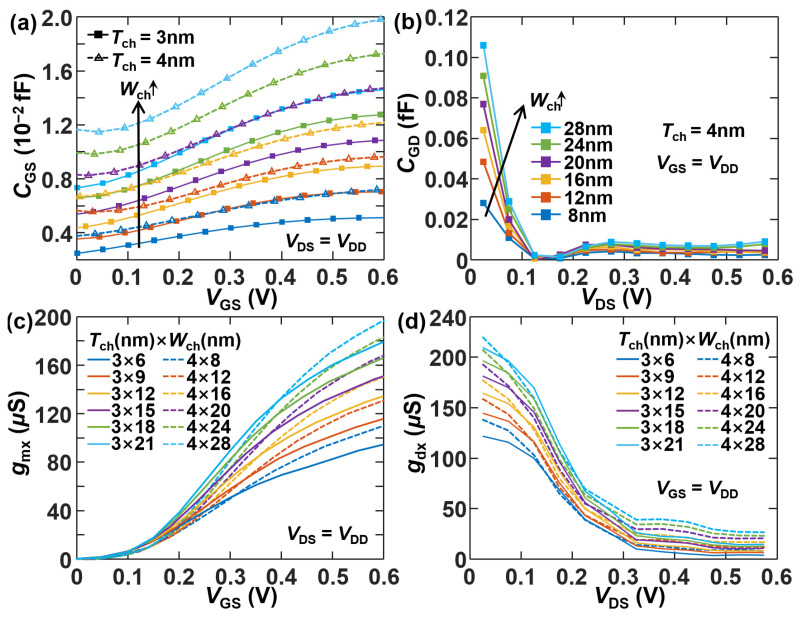 Figure 8
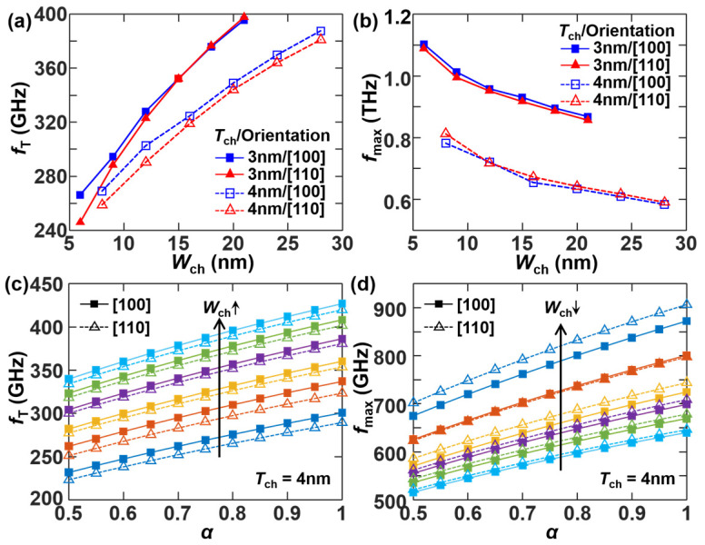 Figure 9
- —National Natural Science Foundation of China
- —Zhejiang Provincial Postdoctoral Science Foundation
- —Zhejiang Provincial Natural Science Foundation
Peer Reviews
No public reviews on file for this paper yet. If you reviewed it on a platform where reviews are public (OpenReview, ICLR, NeurIPS, ICML), you can paste yours below so the community can read it here.
Videos
No videos yet. Explain this paper in a talk, walkthrough, or lecture? Add one.
Taxonomy
TopicsAdvancements in Semiconductor Devices and Circuit Design · Ferroelectric and Negative Capacitance Devices · Radio Frequency Integrated Circuit Design
1. Introduction
The relentless advancement of wireless communication systems, the Internet of Things (IoT), medical imaging, military and aerospace applications has imposed unprecedented demands on the high-frequency performance of CMOS integrated circuits (ICs) [1,2,3]. Particularly, the transition toward 6G and beyond requires carrier frequencies extending into the terahertz range, which imposes even more stringent requirements on the high-frequency figures-of-merit of CMOS ICs [4]. To realize high-efficiency wireless applications and advanced terahertz detection at such frequencies, it is essential to characterize non-linear carrier dynamics and phase transitions using rigorous physical models [5].
As the cornerstone of CMOS technology, transistors must simultaneously deliver high drive current and low parasitic losses to meet the increasingly challenging requirements of advanced technology nodes [6]. While FinFETs have served as the foundation of CMOS ICs for over a decade, their inherent limitations in gate electrostatic control, channel width scalability, and current drivability have prompted the exploration of lateral gate-all-around (LGAA) architectures for next-generation transistors [7,8,9]. In particular, stacked silicon (Si) nanosheet (NS) LGAA-FETs, with their enhanced gate control, higher effective channel width, and improved short-channel immunity, are widely regarded as the most promising successor of FinFET to extend Moore’s Law beyond 2 nm technology node [10,11,12]. On one hand, the aforementioned advantages may help reduce the drain field penetration and output conductance to maintain signal integrity, making the device structure ideal for both logic and analog/RF applications [13,14]. On the other hand, the intricate multi-stack structure can introduce more parasitic capacitances (Cpara) and resistances (Rpara) that degrade RF performance metrics such as cutoff frequency (fT) and maximum oscillation frequency (fmax) [15,16]. However, existing studies on stacked Si NS LGAA n-type FETs (nFETs) have predominantly focused on DC performance for logic applications [17,18,19,20]. The channel width, thickness, and crystal orientation configurations of the NS channel have been demonstrated to significantly influence carrier mobility and DC characteristics [21,22,23]. Spacer engineering has been proposed to decouple gate electrostatic control from parasitic coupling [24,25,26]. For example, dual-k spacers consisting of low-k outer layers and high-k inner layers have shown promise in reducing Cpara and OFF-state leakage without compromising short channel immunity [25,26]. Nevertheless, their impact on the RF performance of Si NS LGAA-nFETs has to be analyzed in conjunction with the interdependent effects of channel geometry, crystal orientation, and contact materials. While recent studies, often utilizing commercial TCAD tools such as Synopsys Sentaurus [27,28], have made significant progress in analyzing RF performance, a holistic analysis of silicon nanosheets that integrates these parasitic effects with a more fundamental quantum transport simulation (NEGF) remains underexplored. Addressing parasitic effects together with quantum effects remains a critical challenge for sub-2 nm node RF applications. Prior works explored the RF-oriented design of Si NS LGAA-FETs with the help of commercial solvers like Sentaurus and specialized field solvers like Raphael [29,30,31], but they often oversimplified the quantum transport properties, such as sub-band splitting and non-parabolicity, which are pivotal for sub-2 nm channels. This necessitates the development of a quantum-accurate, parasitics-aware simulation framework that bridges carrier transport with device high-frequency response. While industry-standard compact models, such as the BSIM-CMG, are widely used for circuit-level design, they increasingly rely on quantum-mechanical corrections to account for nanoscale phenomena. High-order simulation frameworks like the NEGF method are critical for benchmarking these compact models, providing the physical basis for their parameter extraction in the absence of experimental data. The framework presented in this work bridges the gap between fundamental quantum transport and technology pathfinding, ensuring that the predictive design rules for sub-2 nm nodes are grounded in rigorous physics.
This article is a revised and expanded version of [32]. Based on the non-equilibrium Green’s function (NEGF) formalism, this work demonstrates a holistic simulation framework that integrates dissipative quantum transport, parasitics modeling, and RF performance evaluation for stacked Si NS LGAA-FETs. Instead of the widely used effective mass approximation model [33,34], a two-band k·p Hamiltonian is employed so that the effects of non-parabolicity, sub-band splitting, and quantum confinement on conduction band structure can be captured more explicitly [32,35]. Considering different configurations of channel dimensions, crystal orientation, dual-k spacer, and contact materials, parasitic effects and RF figures-of-merit are analyzed systematically for the sub-2 nm technology node. The remainder of this paper is organized as follows: Section 2 details the device structure, parasitic modeling, and the complete simulation framework. Section 3 presents and analyzes numerical results on parasitics and device performance metrics. Section 4 concludes the work.
2. Modeling and Simulation Framework
2.1. Device Structure Modeling
Figure 1a and Figure 1b present the three-dimensional (3-D) and cross-sectional schematics of a Si NS LGAA-FET structure, respectively, where all parasitic resistance and capacitance components are explicitly depicted. The x–, y–, and z–coordinate axes align with the device’s length (transport direction), width, and height/thickness, respectively. The metal contacts are positioned atop the source (S)/drain (D) epitaxial (EPI) and the gated regions, with silicide serving as an interfacial layer at the S/D contact. A dual-k spacer consisting of Si_3_N_4_ and HfO_2_ is deposited within the gaps between metal contacts, encapsulating the entire extension (EXT) region. The geometric parameters of the device are defined and summarized in Table 1, whose default values are configured to comply with sub-2 nm node specifications according to the 2023 International Roadmap for Devices and Systems (IRDS) [6].
2.2. Parasitic Components Modeling
The total Cpara arises from the electrostatic coupling between various conductive regions of the device, as illustrated in Figure 1, which can be broken down into several key components: the contact-to-contact capacitance, gate-to-contact capacitance, gate-to-EPI capacitance, and gate-to-EXT capacitance. These components can be modeled using parallel-plate (Cpar), perpendicular-plate (Cper), and co-planar-plate (Cpi) capacitors models, with their geometric configurations depicted in Figure 2a and Figure 2b, and Figure 2c, respectively.
To clarify the field-coupling topology of the parasitic capacitance network illustrated in Figure 1b, the labeled components are described below from the top of the device to the substrate. The highest red symbol represents the parallel-plate capacitance formed between the inner vertical sidewalls of the two metal contacts. Moving down, the green symbols represent the contact-to-gate and contact-to-S/D EPI fringing perpendicular-plate capacitance. It captures the electrostatic coupling between the vertical sidewall of the metal contact and the top horizontal surfaces of the gate electrode and S/D epitaxy. In the middle region of the structure, the red symbol represents the parallel capacitance formed between the vertical sidewalls of the gate electrode and the S/D EPI. This is a major component of the gate-to-S/D parasitic coupling. At the lower levels near the nanosheet channels, the multiple green symbols represent the perpendicular fringing capacitances between the gate stack and the S/D extension regions across the inner spacers. These Cper components model the fringing fields emanating from the gate to the extension regions that are not directly parallel. In addition, all the purple symbols represent the coplanar capacitance components between different conductive surfaces, contributed by the coupling of contact-to-contact, contact-to-S/D EPI, and gate-to-S/D EPI regions.
Cpar is calculated as εlw/d, where ε represents the constant and uniform permittivity of the dielectric material between two parallel conductive plates with length l, width w, and separation distance d. Leveraging conformal mapping and elliptic integral techniques, both Cper and Cpi can be calculated via an inclined-plate capacitor model [36]. The inner capacitance between two conductive plates inclined at an angle φ is formulated as
where φ is π/2 and π for Cper and Cpi, respectively. K(k) is the complete elliptic integral of the first kind, and the modulus k is given by
and .
The minimal distances of the plates to the origin are r1 and r2, the lengths of which are l1 and l2, respectively. Substituting the corresponding values of φ, r1, r2, l1, and l2 into (2) for Cper and Cpi based on Figure 2b,c, we have
As illustrated in Figure 1, the total Rpara can be divided into contact resistance (Rcon), S/D EPI resistance (Repi), spreading resistance (Rsp), and S/D EXT resistance (Rext). Rpara is modeled as the Rcon in series with the parallel combination of three identical branches, one for each nanosheet channel. Each of these branches consists of the series combination of the Repi, Rsp, and Rext. In our framework, Rext can be well handled by the dissipative NEGF simulation; the other extrinsic components are modeled analytically based on established formulas. Repi and Rsp can be calculated by
and
where ρSD is the bulk resistivity of n-doped Si. Rsp results from the mismatch of current pathway at the spreading region from sheet EXT to bulk EPI.
Rcon arising from the current crowding effect and the Schottky barrier (SB) at the contact/Si interface, is calculated via transmission line model (TLM) as
where ρSH is the n-Si sheet resistivity, and both ρSD and ρSH can be calculated from the electron mobility via the Masetti model [37]. ρcon is the contact resistivity, and it is determined by the competition of thermionic emission (TE), field emission (FE), and thermionic-field emission (TFE) at the SB region, as illustrated in Figure 2d. We have
where
the effective Richardson constant A* is expressed as
where φ_B_ and E_f_ are the SB height and the Fermi level, respectively.
2.3. NEGF-Based Simulation Framework
The comprehensive set of physical parameters, material constants, and simulation targets utilized in our numerical framework is summarized in Table 2.
The detailed execution flow and the hierarchical self-consistent iteration procedures of the in-house dissipative NEGF-Poisson solver are outlined in Table 3.
Figure 3 presents our modeling and simulation framework, designed to holistically evaluate the performance of stacked Si NS LGAA-nFETs by linking quantum transport with extrinsic parasitic effects. Our methodology is to first use our in-house developed NEGF simulator to yield the intrinsic device characteristics, which simultaneously accounts for Rext and quantum capacitance effects. These intrinsic results are then combined with the analytically modeled extrinsic parasitic components to evaluate the final RF figures-of-merit. The simulation workflow iteratively solves the NEGF and Poisson’s equations through an outer loop for achieving self-consistent distributions of carrier density and electrostatic potential, where the reduced-order mode-space method is adopted to reduce the computational load [38]. Using the unitary transformation matrix constructed by the reduced basis, the two-band k·p Hamiltonian, self-energies, and Green’s functions are computed in a reduced-order mode-space for each energy grid. Electron–phonon interactions are incorporated through the self-consistent Born approximation [39], where the retarded and lesser self-energies of acoustic and optical phonon scattering are coupled with Green’s functions in the expressions, requiring an inner iteration loop to realize self-consistency.
As illustrated in the modeling and simulation framework in Figure 3, the tool is structured as a hierarchical evaluation system for advanced technology nodes. The physical core of the framework is the dissipative NEGF engine, which addresses the fundamental transport limits of sub-2 nm nanosheets. This engine utilizes a two-band k·p Hamiltonian, which is discretized using the finite difference method across all three spatial directions to accurately capture non-parabolicity and sub-band splitting. To ensure physical rigor while maintaining computational tractability, a reduced-order mode-space technique is implemented via a unitary transformation matrix. Conceptually, the framework bridges pure transport physics and RF engineering through two nested loops: (i) an inner self-consistent Born loop to model carrier energy relaxation via acoustic and optical phonon scattering; and (ii) an outer Poisson loop to achieve electrostatic self-consistency across the 3-D device domain. Furthermore, the framework integrates extrinsic parasitics derived from the TLM for resistances and conformal mapping with elliptical integrals for capacitances. Technically, the calculated parasitic resistances are integrated as voltage-drop elements that self-consistently modify the effective boundary potential of the NEGF solver, ensuring that the finalized RF figures-of-merit (f_T_, f_max_) incorporate both intrinsic quantum limits and structural parasitic losses.
Furthermore, key RF figures-of-merit, including extrinsic transconductance (gmx), output conductance (gdx), fT, and fmax, are evaluated via
R_S_ and R_D_ denote the source and drain resistances, respectively, and they are equal to half of the total resistance under the assumption that they are symmetric. R_G_ is the gate metal resistance. C_GG_ is the gate capacitance and can be treated as the sum of parasitic and oxide capacitance [29].
All the simulation parameters are determined according to Table 1 and Table 2 and the device performance specifications in the 2023 IRDS [6]. For high-performance applications at a sub-2 nm node, the OFF-state current (I_OFF_) is targeted at 10 nA, the supply voltage (V_DD_) is set to 0.6 V, and the operational temperature T is maintained at room temperature (300 K).
3. Results and Discussion
3.1. Intrinsic Quantum Transport Properties and DC Characteristics
The energy–wave vector (E-k) dispersion curves of different conduction band sub-bands are shown in Figure 4 for a Si NS channel with 3 nm × 21 nm cross section, obtained from the two-band k·p Hamiltonian. Figure 4a,b compares the effects of channel orientations [100] and [110], revealing significant differences in band curvature, degeneracy, and subband splitting. For both orientations, the conduction band minimum resides at the Γ point and is projected from the two Δ valleys on the <001> axis, whose sub-bands dominate the electron transport properties. A valley splitting slightly below 0.17 eV is observed in both cases, identifying the energy level of the second lowest valley minimum contributed from the valleys on the <100> and <010> axes. While Δ_<100>_ and Δ_<010>_ valleys are projected onto the [100]-channel with 2-fold degeneracy, the projection onto the [110]-channel merges these valleys near the X point, leading to coincident primed sub-bands with 4-fold degeneracy. Moreover, the [110] orientation results in larger density-of-states (DOS) and lower electron effective mass.
Figure 5 presents the cross-sectional ON-state electron density distributions in the y–z plane, for NS Si channels with different orientations and dimensions, which are obtained from the dissipative NEGF simulations. For both channel orientations, two prominent conductive layers with high electron concentration emerge adjacent to the vertical sidewalls (aligned with the thickness direction). While the [100]-channel exhibits stronger electron density localization near the midpoint of channel sidewalls, electron density maxima shift toward the four corners in the [110]-channel. This is the consequence of the valley degeneracy phenomenon depicted by Figure 4. Enlarging the cross-sectional area reduces the maximum electron density and enhances spatial uniformity, reflecting mitigated electrostatic confinement. It should be noted that while quantum effects may be addressed phenomenologically in single-device current-voltage (I-V) characteristics, their dominance is clearly observed in the performance sensitivity to structural scaling. For example, the non-linear shifts in current and capacitance as nanosheet thickness varies are intrinsic manifestations of sub-band splitting and confinement, physics that our NEGF framework captures inherently, offering predictive capabilities that classical drift–diffusion models lack without extensive recalibration.
Figure 6a and Figure 6b present the NEGF simulated transfer and output characteristics, respectively, for a [110]-oriented Si NS LGAA-nFET with a 3 nm × 21 nm sheet cross section. It is observed that I_D_ is saturating as VDS approaches VDD, and an ON–OFF ratio higher than 8 × 10^3^ can be achieved for VDD = 0.6 V and IOFF = 10 nA. A subthreshold swing (SS) of ~76 mV/dec is extracted, indicating effective gate control.
3.2. Extrinsic Parasitics Effects and RF Performance
Figure 7a illustrates the dependence of ρcon on NSD at the S/D contact/n-Si interface for SB height ranging from 0.1 to 0.8 eV. In the low doping regime where NSD < 2 × 10^19^ cm^−3^, TE governs the interfacial carrier transport, resulting in relatively high ρcon values (>10^−8^ Ω·cm^2^) constrained by the SB height. As NSD increases to a moderate level, TFE becomes the dominant conduction mechanism, causing a gradual reduction in ρcon with higher doping densities. Within this range, a target ρcon of 5 × 10^−9^ Ω·cm^2^ is achievable for SB heights ≤ 0.3 eV. For the degenerate doping case (NSD > 4 × 10^20^ cm^−3^), ρcon exhibits a sharper decline due to FE-dominated tunneling through the thinned SB. Notably, the effect of SB height diminishes progressively with increasing NSD. Figure 7b demonstrates that the total Rpara can be reduced by the increase in sheet dimensions and S/D doping level, owing to enhanced current-carrying capacity and improved contact characteristics. Figure 7c analyzes the total Cpara modulation with the effects of spacer materials and Lext. It indicates that increased Lext and lower-k spacer materials effectively suppress Cpara by weakening the capacitive coupling between conductive plates. Considering a dual-k spacer architecture combining Si_3_N_4_ (low-k) and HfO_2_ (high-k) with thickness fraction α allocated to Si_3_N_4_, Figure 7d shows its impact on the total Cpara for various NS cross-sectional sizes. The competition between gate leakage suppression and Cpara minimization can be balanced by a proper α. Additionally, the expansion of the channel cross-section results in larger Cpara because of reduced fringing field distances between the gate and EXT regions. To verify the accuracy of our parasitic models, independent validation points from recent literature are incorporated as scatter symbols in Figure 7b,c. Specifically, our calculated parasitic resistances show consistent scaling trends with the 3 nm and 1.5 nm benchmarks in [16], while our capacitance results for various dielectric spacers exhibit an extraordinary numerical match with the results reported in [30,31]. This cross-verification confirms that our simulation framework accurately captures the electrostatic coupling and transport physics at the sub-2 nm node.
Figure 8a and Figure 8b present CGS-VGS and CGD-VDS characteristics at VDS = VDD and VGS = VDD, respectively, for different cross-sectional sizes of the NS channel. Both CGS and CGD exhibit approximately direct proportionality to NS width and saturate at high biasing conditions. However, while CGS increases sublinearly with increasing VGS, CGD decreases inversely with VDS, saturating to a minimum value at high VDS. Figure 8c and Figure 8d show the similar trends of gmx-VGS and gdx-VDS to those of CGS-VGS and CGD-VDS, respectively, for various cross-sectional areas of the NS channel. A higher voltage gain (gm/gd) is achieved by a smaller channel cross-section, exceeding 30 at Tch = 3 nm and Wch = 6 nm. This results from the improvement of gate electrostatics and suppression of the short-channel effect.
Figure 9a,b demonstrates the opposite trends of fT and fmax varying with Wch in a sub-2 nm node Si NS LGAA-nFET. fT increases by ~40% as Wch widens, driven by the enhancement in transconductance. Conversely, fmax decreases by ~35% over the same Wch range due to increased parasitic resistance in narrow channels. A thinner NS channel (Tch = 3 nm) is beneficial for improving operation frequency owing to enhanced gate control. The channel crystal orientation [100] slightly outperforms [110], achieving overall larger fT and fmax, and this is attributed to the lower DOS and thereby weaker scattering in the electron transport. Figure 9c,d further demonstrate that both fT and fmax are promoted by the increase of α, and [110] channel orientation helps improve fmax for thicker NS channels (Tch = 4 nm). In general, Figure 9 reveals the potential applications of sub-2 nm Si NS LGAA-nFETs at millimeter-wave and terahertz frequencies.
It is worth noting that while the extracted f_T_ and f_max_ reach the THz range, the use of the quasi-static approximation (i.e., solving the Poisson equation) remains physically justified. This is because the characteristic dimensions of the sub-2 nm LGAA-FET (~100 nm) are significantly smaller than the electromagnetic wavelength at 400 GHz (ranging from 750 μm in vacuum to hundreds of micrometers in dielectric media). In such a deep sub-wavelength regime, retardation and distributed effects across the individual device are negligible, ensuring the reliability of the self-consistent NEGF-Poisson framework.
4. Conclusions
In summary, this study provides an integrated parasitics-aware quantum transport framework to evaluate the RF performance of sub-2 nm stacked Si NS LGAA-nFETs. By combining a two-band k·p model and dissipative NEGF simulations with a detailed parasitic network analysis, this work characterizes the coupled effects of channel geometry, crystal orientation, and dual-k spacers on key RF figures-of-merit. The results identify a critical design trade-off where scaling W_ch_ and T_ch_ enhances voltage gain and fmax, whereas a wider channel is required to optimize f_T_. Furthermore, [100] crystal orientation is shown to mitigate electron–phonon scattering, thereby improving f_max_ compared to [110] configurations. Our analysis suggests that the implementation of dual-k spacers, combined with minimized Schottky barriers and optimized S/D doping, significantly reduces parasitic components, allowing projected f_T_ and f_max_ to approach the terahertz regime. Based on our simulation framework that bridges quantum effects and circuit-level performance, the findings of this work offer meaningful design insights for the development of ultra-scaled RF CMOS technology and highlight the necessity of co-designing quantum transport physics with parasitic models for the potential millimeter-wave applications of stacked-LGAA transistor structures.
The reference list from the paper itself. Each links out to its DOI / PubMed record.
- 1Liu C. Li Z. Yamazaki Y. Herdian H. Wang C. Tian A. Sakamaki J. Nie H. Fu X. Kato S. A 640-Gb/s 4 × 4-MIMO D-band CMOS transceiver chipset Proceedings of the 2024 IEEE Symposium on VLSI Technology and Circuits (VLSI Technology and Circuits)Honolulu, HI, USA 16–20 June 20241210.1109/VLSI Technologyand Cir 46783.2024.10631487 · doi ↗
- 2Matz G. Messerschmidt B. Göbel W. Filser S. Betz C.S. Kirsch M. Uckermann O. Kunze M. Flämig S. Ehrhardt A. Chip-on-the-tip compact flexible endoscopic epifluorescence video-microscope for in-vivo imaging in medicine and biomedical research Biomed. Opt. Express 20178332910.1364/BOE.8.00332928717570 PMC 5508831 · doi ↗ · pubmed ↗
- 3Zhao D.X. Chen Z.H. You X.H. Design and implementation of CMOS millimeter-wave I Cs and 4096 TX/4096 RX very-large-scale integrated phased-array antenna Sci. Sin. Inform.202151505519(In Chinese)10.1360/SSI-2020-0404 · doi ↗
- 4Wang Y. Zhang X. Wang Y. Liu Y. Li J. Chen X. Cui Z. Burokur S.N. Zhang J. Zhao X. Recent advances in metasurfaces: From T Hz biosensing to microwave wireless communications Research 20258082010.34133/research.082040896398 PMC 12395562 · doi ↗ · pubmed ↗
- 5Zhang L. Lv X. Dong Z. Dutta D. Yang L. Ahammed R. Chakraborty A. Wang D. Hu Z. Jiang M. Dynamic polarization control of nonlinear terahertz photoeresponse via topological phase transitions Research 20258089910.34133/research.089941020158 PMC 12460995 · doi ↗ · pubmed ↗
- 6Institute of Electrical and Electronics Engineers IEEE International Roadmap for Devices and Systems 2023 Available online: https://irds.ieee.org/editions/2023(accessed on 1 January 2024)
- 7Loubet N. Hook T. Montanini P. Yeung C.-W. Kanakasabapathy S. Guillom M. Yamashita T. Zhang J. Miao X. Wang J. Stacked nanosheet gate-all-around transistor to enable scaling beyond fin FET Proceedings of the 2017 Symposium on VLSI Technology Kyoto, Japan 5–8 June 2017 T 230T 23110.23919/VLSIT.2017.7998183 · doi ↗
- 8Zheng P. Connelly D. Ding F. Liu T.-J.K. Fin FET evolution toward stacked-nanowire FET for CMOS technology scaling IEEE Trans. Electron Devices 2015623945395010.1109/TED.2015.2487367 · doi ↗