Interfacial Hopping Integral as a Predictive Descriptor for Electron Transport: Saturated Alkane Junctions
Hao Howard Peng, Chih-Hsun Lin, Po-Wei Tung, Chun-Wei Lin, Yen-Chang Chiang, Bon-Shen Wang, Ting-Hsuan Ning, I-Chih Ni, Chih-I Wu, Chun-hsien Chen

TL;DR
This paper introduces a new way to predict electron transport in molecular junctions by measuring the overlap between atomic orbitals at the interface.
Contribution
The interfacial hopping integral (t_eld–mol) is proposed as a predictive descriptor for electron transport in molecular junctions.
Findings
Conductance correlates with molecular tilt across π- and σ-type headgroups.
A tight-binding model matches experimental results and generalizes to various molecular junctions.
Variations in t_eld–mol explain different conductance sets in alkanedithiols.
Abstract
Electron transport across interfaces governs a broad range of fundamental phenomena. Although orbital overlap is recognized as a key determinant, its experimental quantification remains elusive. Here, we establish the interfacial hopping integral (t eld–mol), quantifying orbital overlap between contacting atoms, as a predictive descriptor of single-molecule conductance in a benchmark domain of saturated α,ω-functionalized alkane junctions. Using scanning tunneling microscopy and molecular-junction mapping technique, we correlate conductance with molecular tilt (tilt mol) across π- and σ-type headgroups to extract t eld–mol. We start with single-atom-thick bismuth and lead adlayers on gold, with dominant p-character simpler than gold’s d-orbitals. A tight-binding model incorporating Newns–Anderson–Grimley theory yields conductance heatmaps that qualitatively match experiment results and…
Genes, proteins, chemicals, diseases, species, mutations and cell lines named across the full text — each resolved to its canonical identifier and authoritative record.
Click any figure to enlarge with its caption.
 1
1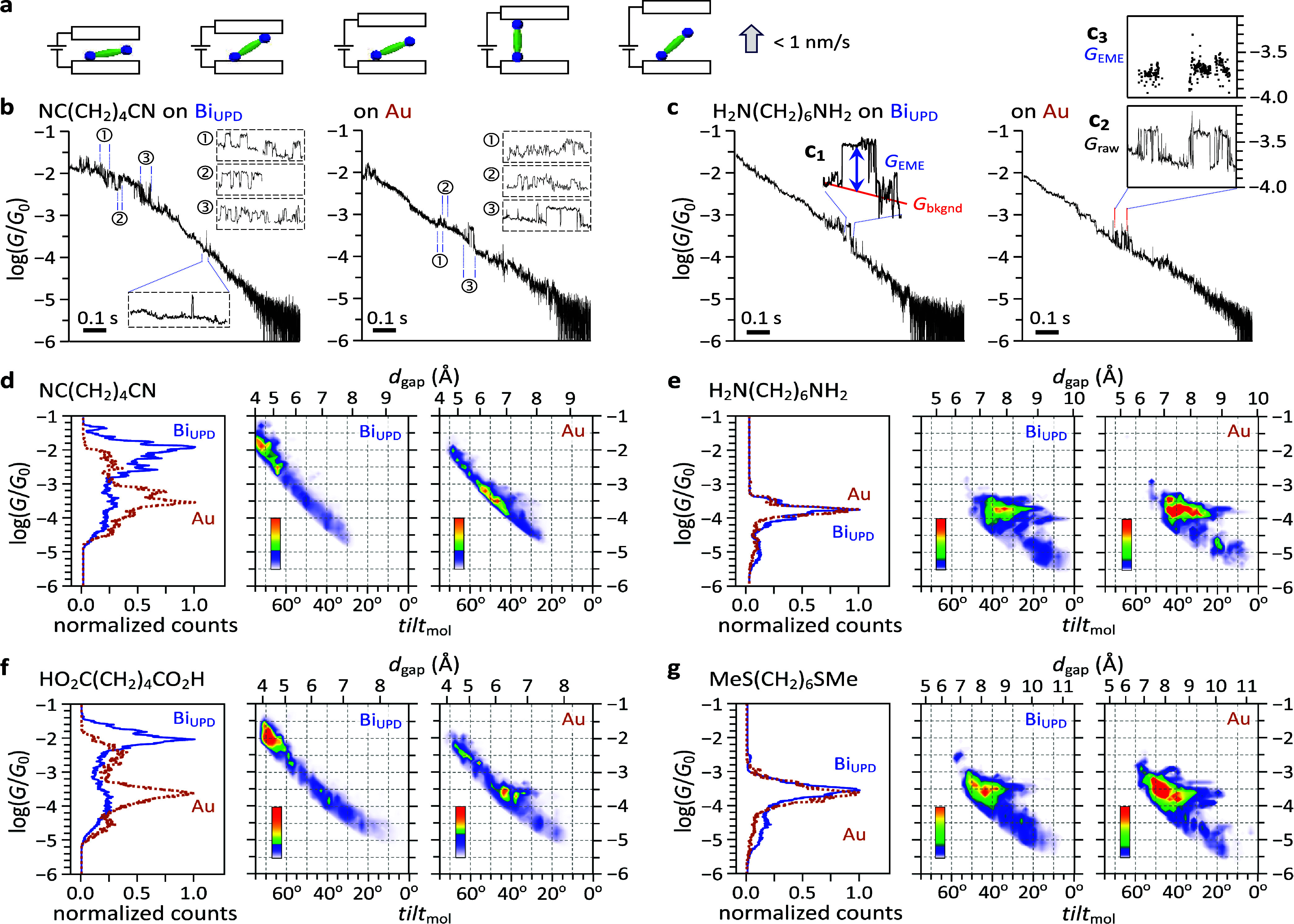 2
2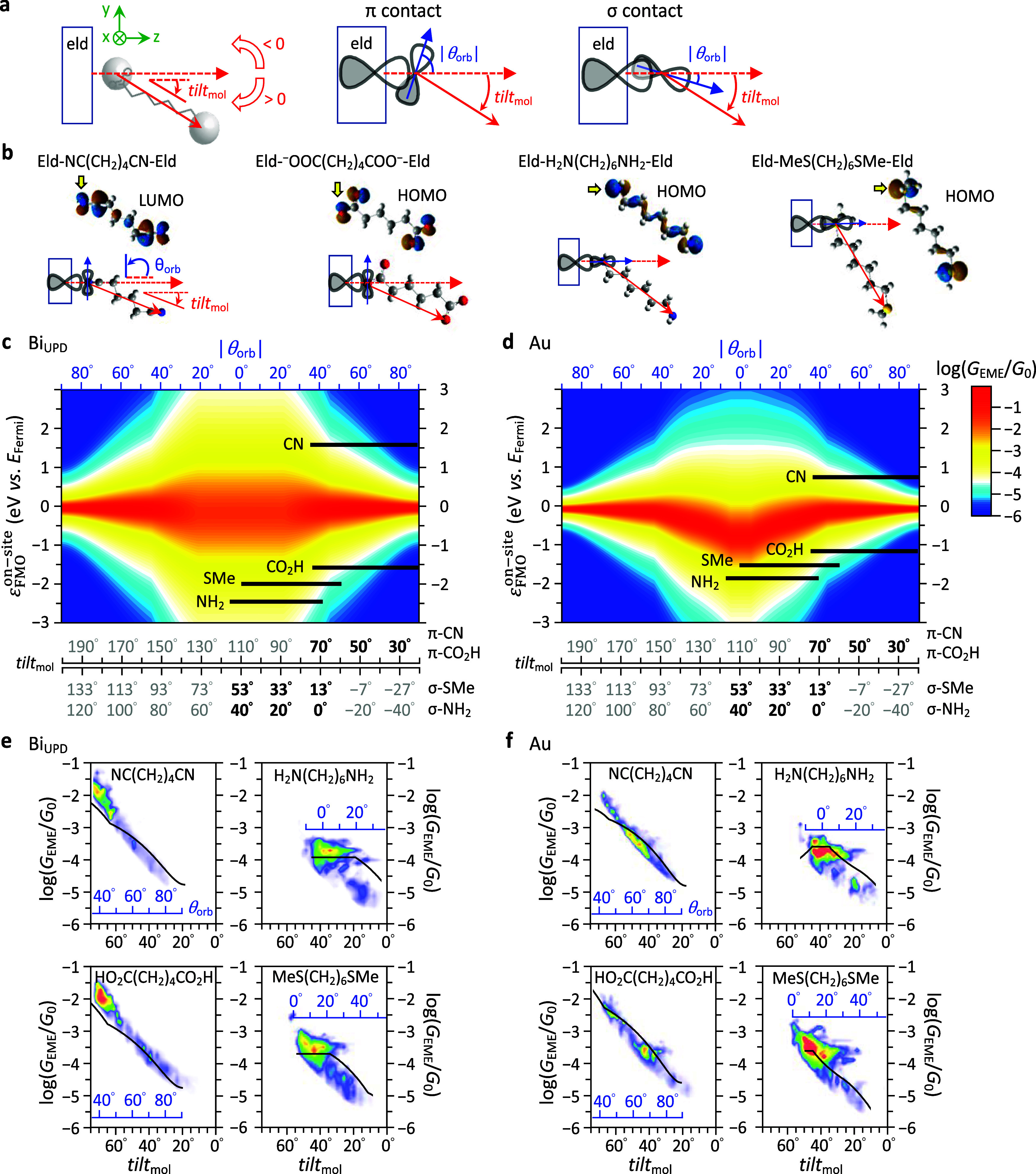 3
3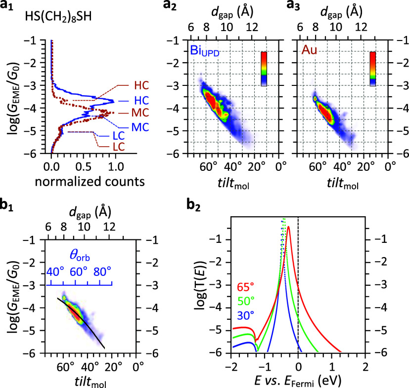 4
4- —National Taiwan University10.13039/501100006477
- —National Taiwan University10.13039/501100006477
- —National Science and Technology Council10.13039/501100020950
- —National Science and Technology Council10.13039/501100020950
- —National Science and Technology Council10.13039/501100020950
Peer Reviews
No public reviews on file for this paper yet. If you reviewed it on a platform where reviews are public (OpenReview, ICLR, NeurIPS, ICML), you can paste yours below so the community can read it here.
Videos
No videos yet. Explain this paper in a talk, walkthrough, or lecture? Add one.
Taxonomy
TopicsMolecular Junctions and Nanostructures · Force Microscopy Techniques and Applications · Electrochemical Analysis and Applications
Introduction
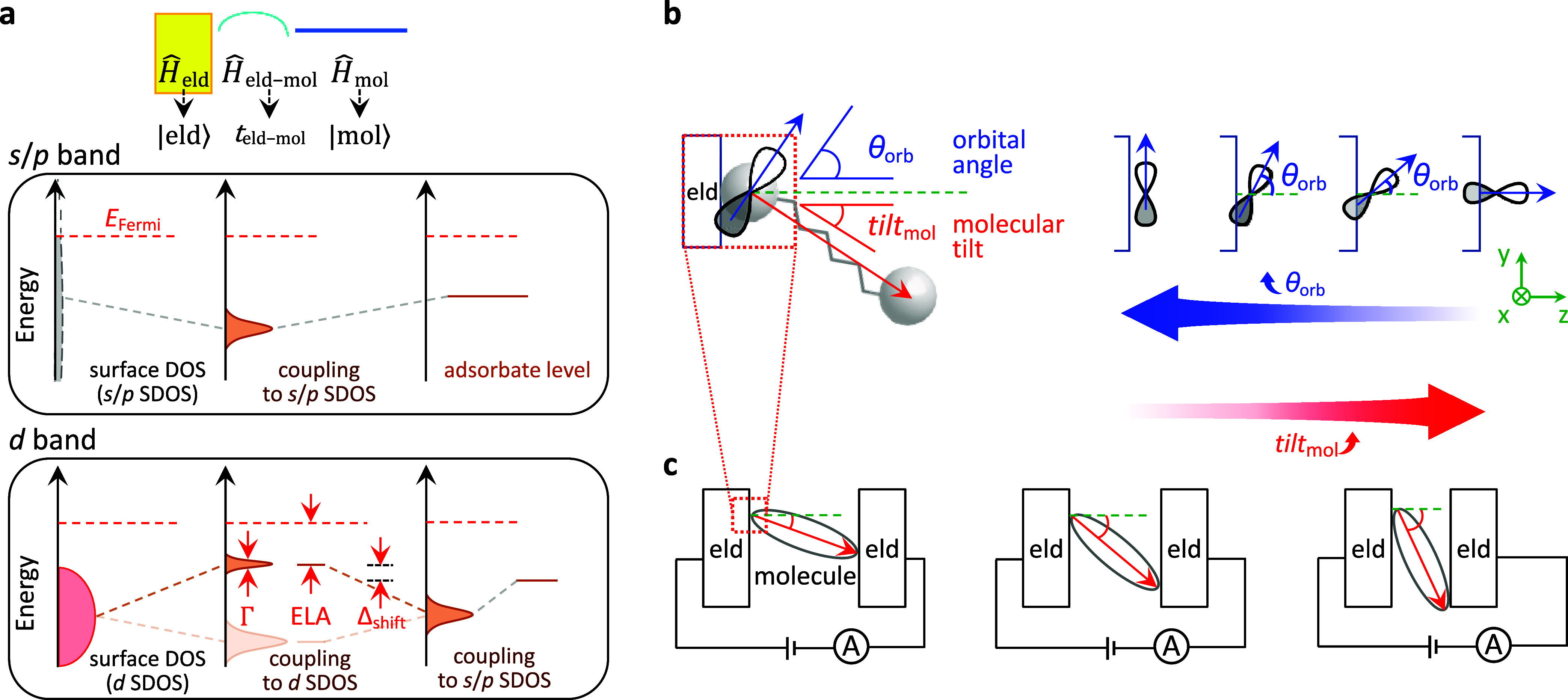
Electron transport across electrode-molecule interfaces underpins a wide spectrum of scientific disciplines. While the hopping integral is well recognized as essential for interfacial electron transport, its measurement remains inaccessible due to the lack of any observable tunable by interfacial parameters. Theoretical models often use an off-diagonal Hamiltonian (Ĥ_eld–mol_, Figurea) to describe the electrode-molecule contact. Within this framework, the interfacial hopping integral (t eld–mol = ⟨Φ_eld_|Ĥ_eld–mol_|Φ_mol_⟩) quantifies this coupling and governs transport efficiency.? In a nearest-neighbor tight-binding approximation, t eld–mol reduces to the overlap of primitive atomic orbitals (AOs) at the contact (Figureb). We propose t eld–mol as an intuitive descriptor for electron transport and develop an experimental framework to benchmark its predictive power within saturated alkane junctions.
Interfacial hopping integral and its dependence on molecular tilt angles. (a) Schematic of Hamiltonians for electrode–molecule interfaces illustrating discrete adsorbate level coupled with electrodes of (middle panel) s/p and (lower panel) d surface bands. Symbols Δshift, Γ, and ELA denote energy shifts arising from adsorption, level broadening, and energy difference relative to the electrode E Fermi, respectively. (b) Diagrams illustrating θ orb, the angle of an atomic p orbital with respect to the surface normal. θ orb determines the extent of orbital overlap at the interface and is directly related to the molecular tilt angle (tilt mol) in the laboratory frame. The depicted orientation of the p orbital relative to the headgroup-carbon bond is a conceptual illustration based on the calculated FMOs for representative molecular headgroups employed in this study (see Figures b or S16). (c) Illustration of molecular tilt mol in an EME junction. Reducing the gap spacing increases tilt mol angles.
Electric conductance across an electrode-molecule-electrode (EME) junction (Figurec) represents an observable of electron transport. A small change in t eld–mol might affect the interfacial transport pronouncedly because the junction conductance roughly scales as the fourth power of t eld–mol,? based on Fermi’s golden rule inherited in the Breit-Wigner type electron transmission? for the Landauer formula.? Apparent parameters enabling the modulation of t eld–mol via orbital overlap include the interatomic distance (d nn) and the angle between the AOs (θ orb) by a tilt of the molecular chain (tilt mol). In practice, d nn cannot be adjusted with reasonable control, whereas it is experimentally feasible for the latter. Figurec illustrates that tilt mol (and thus θ orb, Figureb) increases by narrowing the electrode gap spacing (d gap) which is adjustable using a piezo-driven tip of a scanning probe microscope. ?−? ? ? ? ? ? ?
Conductance measurements have been performed for EME platforms with monolayer assemblies or single molecules. We choose single-molecule junctions to avoid collective effects present in monolayers, for example, a very limited tilt mol range due to steric hindrance in closely packed molecules, extra tunneling paths via neighboring molecules, ?−? ? and interface dipoles that shift the adsorbate’s frontier molecular orbital (E FMO).? To configure single-molecule junctions, we adapt the molecular-junction mapping (MJM) technique developed by Chang and co-workers? with a tip of scanning tunneling microscope (STM) moving slowly (<1 nm/s) toward or away from the substrate. The slow motion exerts nearly no disturbance to the junction such that the measurement resembles a survey over the EME gap spacings where the bridged molecule can freely adjust suitable tilt mol and binding geometries? (Figuresc and ?a).
Mapping conductance and molecular tilt via MJM technique. (a) Schematic of the MJM setup. An STM tip moves slowly to modulate the gap spacing between electrodes and allow free formation of EME junctions. (b, c) Representative conductance traces of (b) NC(CH2)4CN and (c) H2N(CH2)6NH2 measured on BiUPD and bare Au electrodes. The magnified sections and insets in panel b emphasize the frequency of conductance jumps and their dwell-time durations, which explain the 2D conductance histograms presented in panel d. Insets (c1–c3) illustrations of conductance assignment: (c1) reported G EME value, (c2) raw conductance section, (c3) background-subtracted section, where G EME is extracted from the plateau level following a spontaneous conductance jump above the tunneling background (G bkgnd); accordingly, the background-subtracted values in c3 are lower than the raw data in c2. (d–g) Normalized conductance histograms plotted against tilt mol and d gap for (d) NC(CH2)4CN, (e) H2N(CH2)6NH2, (f) HO2C(CH2)4CO2H, and (g) MeS(CH2)6SMe. d gap is derived from G bkgnd and tilt mol is calculated from d gap and the full-extended molecular length. Other conditions: solvent, trimethylbenzene; tip moving speed, 0.50 nm/s. Upper limits for the color-bar scales (values × 103): BiUPD: (d) 3.0, (e) 0.9, (f) 2.0, (g) 1.8; bare Au: (d) 3.0, (e) 0.5, (f) 1.3, (g) 0.7.
Electrode material offers another dimension to study t eld–mol, though practical choices are limited to coinage metals, with gold overwhelmingly preferred for its unparalleled malleability in forming EME junctions and for its resistance to oxidation. However, valence states of transition metals feature d-orbitals, which are more complicated than p-orbitals in terms of shapes and total amounts of magnetic quantum number . Additionally, s/p-bands are flat compared to d-bands. Figurea highlights this contrast: on s/p-band electrodes the adsorbate level is broadened, whereas on d-band electrodes it splits into bonding and antibonding states. ?−? ? Hence, we start from electrodes with dominant p-character by placing a monoatom-thick Bi or Pb adlayer onto gold electrochemically via underpotential deposition (UPD, abbreviated as Bi_UPD_ ? and Pb_UPD_ ?).
To comprehensively assess t eld–mol, we examine homologous series of α,ω-alkanes with σ- and π-type headgroups. These polymethylene backbones bear E HOMO and E LUMO located further away from E Fermi than E FMO of the electrode-headgroup adsorbate state, allowing the use of a single-level model to elucidate their transport behavior. Because the transporting FMO is largely localized on the headgroup (see Figuresb or S16), the orbital overlap with the electrode can be depicted directly. This interaction can be defined by considering the AOs of the contacting electrode atom and the headgroup atom, thus expressing t eld–mol specifically as t eld–head. Accordingly, the present framework models junctions in which transport is dominated by a single headgroup-localized interfacial state, and where tilt mol serves as a geometric descriptor within the MJM analysis.
*Theoretical conductance heatmaps and the predictivity. (a) Translation from molecular tilt angle tilt mol to the degree of electrode-headgroup orbital overlap, where tilt mol is defined as the angle between the surface normal and the molecular axis (solid red arrows, defined as the vector from the headgroup end-atom on the surface to the counterpart). For π and σ-type headgroups, the same tilt mol results in different θ orb and thus different interfacial hopping integrals. (b) FMO of α,ω-alkanes and interfacial-coupling schematic. The FMO for NC(CH2)4CN is LUMO −
and for the others is HOMO. The yellow arrows highlight the FMO densities that contact the electrodes, which are portrayed as p-like orbitals in each schematic. Conductance heatmaps for (c) BiUPD and (d) Au EME junctions. The y axis is εFMO on‑site (eV vs E Fermi), the on-site FMO energy of α,ω-alkanes. The lower x axes are tilt mol for π and σ headgroups, and the upper x axes are θ orb. The θ orb correspondence to tilt mol is sketched for each headgroup. (e, f) Overlaid G EME–tilt mol plots (black solid traces in Figure d,e) with conductance profiles predicted by the black horizontal lines on the heatmaps (Figure 3c,d). The tilt mol range of the conductance profile is limited by steric hindrance. Color scale upper limits for (e, f) are identical to the corresponding electrode–headgroup pairs in panels (d–g) of Figure .*
Finally, we integrate Newns–Anderson–Grimley model for molecular adsorption ?,? with the Slater–Koster? and Harrison ?,? formalisms for orbital coupling to construct a tight-binding transporting framework at the atomic orbital level. ?−? ? This model highlights the role of t eld–head in electron propagation across EME junctions and produces conductance heatmaps that qualitatively portray junction conductance with the on-site energy of the molecular FMO (ε_FMO_ ^on‑site^) using t eld–head as the key descriptor.
Results and Discussion
Conductance-Molecular Tilt Mapping
MJM conductance traces are plotted semilogarithmically versus time (Figureb,c). The background current decays exponentially with the EME gap distance (d gap), described by i bkgnd = G bkgnd × V bias ∝ V bias e^–βd gap ^ where β is a tunneling decay constant. Therefore, i bkgnd can be used to extract d gap (Supporting Information, Section 2-2). In the logarithmical plots (Figureb,c), the MJM baselines appear linear-like because d gap changed with a constant tip motion (0.50 nm/s). The signature of spontaneous EME formation is the appearance of discrete conductance jumps superimposed on the tunneling background (e.g., Figurec_1_). The value of EME conductance (G EME) is determined by subtracting the tunneling background from the conductance trace plateau (e.g., Figurec_2,3_). Data are pooled into a 1D histogram to reveal the most probable G EME. Plotting G EME against another measurable parameter yields a 2D histogram revealing correlations hidden in 1D analysis. For example, 1D histograms of NC(CH_2_)4_CN (Figured) show that the most probable peak on Bi_UPD is two-order-of-magnitude more conductive than that on bare Au electrodes. Incorporating tilt mol confers 2D histograms and reveals that the conductance peak on Bi_UPD_ in the 1D histogram occurs mainly at tilt mol ∼ 70°, whereas on bare Au, it occurs at a smaller tilt mol near 45°, with a shoulder at ∼53°. These findings match jump frequency and dwelling time distribution (e.g., Figureb) although jumps are stochastic and intermittent throughout an MJM trace.
Panels d,f and e,g of Figure exemplify π- and σ-type headgroups, respectively. NC(CH_2_)4_CN and HO_2_C(CH_2)4_CO_2_H (π-type headgroups, Figured,f) exhibit similar trends that their most probable G EME takes place at larger tilt mol on Bi_UPD and is significantly more conductive on Bi_UPD_ than on Au. Conversely, σ-type headgroups (−NH_2_ and −SMe, Figuree,g) yield comparable conductance on Bi_UPD_ and Au electrodes. Their G EME values appear insensitive to increased tilt mol, in contrast to the increasing patterns observed for π-type headgroups. Near-vertical orientation (tilt mol 10–20° for H_2_N(CH_2_)6_NH_2, 20–30° for MeS(CH_2_)_6_SMe) yields G EME ∼one-order-of-magnitude smaller than dominant peaks in 1D histograms, corresponding to the low conductance set assigned in literature reports.?
In Figured–g, G EME increases with tilt mol at small angles. At larger tilt mol, the increase persists in Figured,f but levels off in Figuree,g. Intriguingly, for H_2_N(CH_2_)8_NH_2 (Figure S7), a distinct downturn appears: for tilt mol > 30°, G EME decreases by nearly half an order of magnitude. This decline likely continues at larger tilt mol (i.e., narrower d gap), but is experimentally masked by the rising background tunneling current (i bkgnd), which obscures the smaller molecule-mediated transport current, rendering G EME inaccessible at high tilt mol. These trends presented in this section are also observed on Pb_UPD_ (see Figure S14).
Tight-Binding Transport Model with Headgroup-Orbital Orientation
Under the tight-binding framework, ?−? ? only orbitals overlapping at the electrode-headgroup contact are considered for interfacial propagation. To rationalize the tilt mol-dependence of G EME (e.g., Figured–g) and contrasting behaviors of π- and σ-type headgroups, we apply Harrison’s matrix element V (in eV) ?,? following Slater and Koster? to describe t eld–head
where V includes an orbital structure factor? relevant to the extent of orbital overlap between atoms at a given d nn. V corresponds to the maximal t eld–mol value with the largest orbital overlap at θ orb = 0°.
We derive a t eld–head-integrated quantum transport model from Landauer formalism^2^ (with Meir-Wingreen’s method?) and the Newns–Anderson 1D atom-chain-electrode model.? Equation shows the general expression for G EME under small V bias, i.e., E ≈ E Fermi.
where ε_FMO_ ^on‑site^ denotes the on-site energy of the molecular FMO, Δ_shift_ is the energy shift of the adsorbed FMO (Figurea), E Fermi – ε_FMO_ ^on‑site^ – Δ_shift_ defines the adsorbate energy-level alignment (ELA, Figurea), the prefactor A accounts for intramolecular coupling (for the explicit form, see eq S2), L is the molecular length, and Γ_eld‑head_ ^2^|_ E=E Fermi _ describes the effect of electrode-headgroup coupling strength at E Fermi. Γ_eld–head_ correlates with the extents of orbital overlap (i.e., the hopping integral t eld–head), and is formulated by eq.
ε_eld_ and t eld denote the electrode’s on-site energy (surface band center) and the hopping integral between neighboring sites of the electrode, respectively. The d-band contribution (i.e., Γ_eld–head_) vanishes when E – ε_eld_ lies outside ±2t eld. Substituting eq into eq, and then into eq shows that G EME depends on θ orb, and thus on tilt mol.
The t eld–head-dependent model provides a quantitatively good fit to each MJM-acquired α,ω-alkane G EME data on bare Au, Bi_UPD_, and Pb_UPD_, supporting t eld–head as a quantitative descriptor of single-molecule junction conductance (Figure S12). Equation adopts a nearest-neighbor approximation in which only the direct electrode–headgroup overlap is treated. In practice, additional through-space tunneling pathways (e.g., to nearby nonadjacent atoms at large tilt mol) and local surface roughness are not included and may lead to deviations from a pure cosine dependence. Accordingly, the t eld–head values extracted from fitting should be hereafter interpreted as effective hopping integrals that subsume these unmodeled contributions. Details of the procedures and fitting results are provided in Supporting Information Section 3 and Table S5.
Conductance Heatmaps for Interfacial Electron Transport
Figure presents simulated conductance heatmaps, generated from eqs–? in which the required parameters were obtained by fitting MJM data for NC(CH_2_)4_CN (π-type) and H_2_N(CH_2)6_NH_2 (σ-type); the heatmaps use the average of these two sets of fitted parameters (see footnote d of Table S5). The z-axis value of Figurec,d at each coordinate pair of ε_FMO_ ^on‑site^ and tilt mol represents zero-biased G EME|_ E=E Fermi . Figurea depicts a pair of π- and σ-type headgroups with identical tilt mol, yet their corresponding θ orb orientations differ by ∼90° (the angle between the two blue arrows at the central and right panels). Figurea also illustrates the correlation between the laboratory-frame tilt mol and the molecular-frame θ orb. Steric interactions with the surface constrain the accessible tilt mol range, mainly due to the proximal terminal groups such as the hydrogen atoms in −NH_2 or the methyl group in −SMe. Figureb presents the FMO of α,ω-alkanes and corresponding schematic of interfacial coupling. The FMO responsible for electron transport is LUMO for NC(CH_2_)_4_CN ?−? ? ? and HOMO for the others. The FMO densities that contact the electrodes (indicated by yellow arrows) are portrayed as p atomic orbitals in each schematic.
Figurec, modeled on Bi_UPD_, exhibits G EME contours symmetric about the x-axis. The red and yellow regions below ε_FMO_ ^on‑site^ = 0 are marginally outweigh those above, reflecting the slightly negative-positioned Bi p-band center. This hardly noticeable asymmetry arises because, for adsorbates with ε_FMO_ ^on‑site^ in resonance with the Fermi level (i.e., at ε_FMO_ ^on‑site^ = 0 eV), coupling to the p band shifts the FMOs away from E Fermi, increases their energy offset, and attenuates ELA, thus lowering G EME slightly. As θ orb decreases from 90°, the red zone disperses due to broadened Γ_eld–head_, indicative of enhanced interatomic orbital overlap and strengthened t eld–head. Below θ orb ∼ 30°, this broadening diminishes because inductive effects (i.e., orbital reorientation) ?−? ? energetically align the interfacial p-orbitals and maintain optimal overlap. ?,? Hence, further decreasing θ orb produces negligible additional broadening of the red zone, unlike the trend on Au (Figured, vide infra). According to the fitting results, this inductive reorientation also shortens d nn, strengthening coupling to the Bi_UPD_ 6p _ z _-band. Stronger coupling stabilizes the HOMO and destabilizes the LUMO,? increasing |E Fermi – E FMO| (i.e., a poorer ELA) in both HOMO- and LUMO-dominant transport regimes, ultimately reducing G EME.
Horizontal slices at specific ε_FMO_ ^on‑site^ values are plotted as G EME–tilt mol traces in Figuree,f, overlaid with experimental MJM data. These traces, scaled by G EME ∝ e^–βL^ (eq) to account for molecular-length differences (i.e., the differences in methylene units), agree well with experimental results. For π-type NC(CH_2_)4_CN or HO_2_C(CH_2)4_CO_2_H in Figurec, G EME increases with larger tilt mol, attributed to enhanced nitrogen-6p _ z (Bi_UPD) or monodentate oxygen-6p _ z (Bi_UPD) orbital interactions (see Figuresb or S16). For σ-type H_2_N(CH_2)6_NH_2 and MeS(CH_2_)6_SMe in Figured, G EME rises rapidly as tilt mol moves from 0 to ∼ 30° (specifically, θ orb decreases from ∼40 to ∼20° for −NH_2 and from ∼50 to ∼20° for −SMe) and then levels off, reflecting improved orbital alignment and the inductive effect. Remarkably, while this heatmap is prepared by parameters of −NH_2_/–CN headgroups, the cross sections capture conductance trends for −COOH and −SMe. The strong agreement between heatmap-derived traces and experimental data (Figurec) highlights the generality and predictive capability of the model across diverse headgroups.
Figured, modeled on bare Au, demonstrates how d-bands perturb the s/p-band-based heatmap of Figurec. Compared to Figurec, contours in Figured shift downward, and the red zone becomes V-shaped. These features stem from Au’s low-lying, narrow, and fully filled d-bands. Au-adsorbate interactions splits the adsorbate state into bonding and antibonding states (Figurea), with the antibonding states often found below E Fermi and occupied.? Occupation of this antibonding state counteracts bonding stabilization, leading to a net destabilization termed metal-adsorbate repulsion. ?,?,? An increased orbital overlap toward small θ orb reinforces this repulsive effect, impedes the inductive orbital reorientation, and reduces the tendency for EME junction formation, although the improved ELA does raise G EME.
For a quantitative perspective, Nørskov et al. describe the chemisorption energy (ΔE d–hyb) as?
where the first term represents attractive orbital mixing and the second term represents Pauli repulsion. V denotes the metal-adsorbate coupling matrix element (equivalent to t eld–head), ε_d_ and ε_ab_ are the energies of the metal d-band center and the antibonding state (equivalent to ε_FMO_ ^on‑site^ + Δ_shift_), respectively. α is a positive constant, accounting for the energy penalty of overlapping electron orbitals constrained by the Pauli exclusion principle (namely, orbital orthogonalization), and f d is the d-band filling fraction.?
For metals like Au with fully occupied d-bands (presumably f d = 100%), the attractive term is effectively nullified. However, Abild–Pedersen et al. found that a small fraction of antibonding states remains unfilled.? Hence, Au-adsorbate interactions are dominated by Pauli repulsion, disfavoring EME junction formation despite modest ELA gains. This repulsion suppresses the inductive effect, causing Γ_eld–head_ to broaden gradually with increasing tilt mol. Consequently, Au electrodes reach Γ_eld–head_ saturation more slowly, extending the inductive response over a wider tilt mol range and yielding the V-shaped contour (Figured). Conversely, Bi_UPD_ (f d = 0), free of antibonding penalties, enables rapid Γ_eld–head_ saturation, producing plateau-like conductance behavior and a stronger inductive response. Accordingly, uHC is suppressed on Au (near d ^10^) but prominent on Bi_UPD_ and Pb_UPD_, consistent with stronger filled-d-band repulsion on Au under high-tilt mol configurations that yield larger t eld–head.
For −CN/–COOH headgroups (π-type), G EME–tilt mol trends on Au are similar to those on Bi_UPD_. However, the G EME–tilt mol plots (Figuresd,f and ?e,f) shows that high-tilt configurations occur less frequently on Au (also consistent with the EME events shown in Figureb), likely due to the above-mentioned repulsion at tilt mol > 55°.
For −NH_2_/–SMe (σ-type headgroup), G EME rises as tilt mol increases from ∼5 to ∼35°, reflecting inductive orbital alignment and d nn adjustment. Greater than ∼35°, conductance does not increase and even declines for H_2_N(CH_2_)8_NH_2 (Figure S7).
These conductance heatmaps provide qualitative predictions for each headgroup–electrode pair. Notably, the Bi_UPD_ and Pb_UPD_ benchmark heatmaps are closely similar (Figures S13 and S14), consistent with both being p-character electrodes. Their p-band centers lies slightly below (Bi_UPD_) and above (Pb_UPD_) E Fermi, which subtly shifts the high-conductance region (red zone) toward the lower and upper halves of the heatmap. However, for the headgroups studied here, the fitted ε_FMO_ ^on‑site^ values are away from E Fermi; therefore, this modest landscape shift does not lead to discernible conductance difference.
Using our benchmark systems, four types of headgroups measured on bare Au, Bi_UPD_, and Pb_UPD_, as references, untested pairs can be anticipated from three inputs: (i) the electrode surface DOS (e.g., Figure S10), which shapes the heatmap landscape; (ii) the headgroup’s orbital symmetry (π or σ) and steric constraints, which define the accessible tilt range (bottom x-axis); and (iii) the on-site frontier level, ε_FMO_ ^on‑site^ (y-axis). In our implementation, ε_FMO_ ^on‑site^ values are determined by fits to MJM data (Table S5). For untested systems, qualitative placement follows the dominant frontier orbital: LUMO-dominant (n-type) responses map to the upper half of the heatmap, whereas HOMO-dominant (p-type) responses map to the lower half; within each half, the conductance profiles are closely similar. The Newns–Anderson DOS is represented by a semielliptical form for analytical tractability, differences from the DFT-projected DOS propagate primarily through Γ and the real-part level shift that sets ELA, thereby influencing the absolute conductance scale rather than the trend of tilt angles. An estimate based on Figure S10 suggests that for Au this corresponds to a few-fold uncertainty in G EME, while the G EME–tilt mol dependence governed by t eld–head remains unchanged.
t
eld–head as a Descriptor for Alkanedithiol Junctions
Alkanethiols, renowned for their seminal role in self-assembled monolayers and molecular electronics, have long served as the benchmark for methodological development in single-molecule G EME measurements. ?,? Despite extensive study, reported alkanedithiol G EME values vary widely, ranging from no discernible peak ?,? to one, ?−? ? ? ? ? two, ?,? or multiple ?,?,?−? ? ? ? conductance sets (commonly categorized as high (HC), medium (MC), and low (LC)). This variability is attributed to inherent complexities in junction geometries, binding sites, molecular conformations, measurement schemes, experimental conditions, and data analysis protocols. Quantum transport simulations that typically assign HC to bridge ?,?,? or hollow ?,?−? ? sites and LC to atop sites ?,?,?−? ? predict only modest 2–5-fold ?,? conductance differences, far short of the ∼18–25-fold spread observed experimentally. ?,?,?,?,?,? Wandlowski, Evers, and co-workers proposed that LC has to arise from gauche conformers, which are shorter than the fully extended HC conformation and thus should appear at narrower d gap.? Because STM-BJ traces progress from short to long d gap, this interpretation predicts LC should precede MC/HC within a single trace; yet, in the same paper the authors report that MC never follows LC, nor does HC follow MC.? Comparisons are further hampered because computational studies often employ diverse, model-dependent electrode–headgroup geometries tuned to reproduce individual experimental results, complicating cross-study benchmarking. ?,?,?
By suppressing artifacts (e.g., multimolecule bridging or through-space tunneling), controlling d gap, and correlating G EME with tilt mol, the MJM method employed herein mitigates junction heterogeneity and enables unbiased identification of multiple conductance states in a single measurement.? The resulting 1D histograms and explicit G EME–tilt mol relations motivate a new perspective on this longstanding issue through interpretation with the t eld–head-based model.
MJM-acquired 1d-histograms for octanedithiol (Figurea_1_) show peak values comparable to literature reports; ?,?,?,? accordingly, we label the peaks following the established assignment. ?,?
Figurea_2_,a_3_ show that HC, MC, and LC emerge sequentially as d gap increases, ?,? reflecting increasing θ orb (Figureb_1_). The G EME–tilt mol profiles of octanedithiol mirrors those of π-type headgroups and aligns with the alkanethiol HOMO, which has a π-like lobe at sulfur ?,? (Figure S16). On bare Au, HC and LC are less populated than MC, while Bi_UPD_ shows more pronounced HC. The suppressed HC on Au likely reflects antibonding orbital repulsion.
Conductance-tilt mapping and t eld–head-based model validation for HS(CH2)8SH. (a) MJM-acquired conductance histograms of HS(CH2)8SH on (a1) BiUPD (blue) and Au (brown) electrodes, and corresponding (a2,3) G EME–tilt mol plots showing HC, MC, and LC conductance taking place sequentially with increasing d gap. (b) t eld–head-based modeling. (b1), Simulated G EME–tilt mol profile at εFMO on‑site = −0.57 eV (vs E Fermi) of the heatmap in Figure d, overlaid with MJM data, reproduces the experimental trend. (b2) Associated transmission spectra show that increasing tilt mol broadens Γeld–head, improves ELA, and raises T(E Fermi). These results support t eld–head as a quantitative descriptor of interfacial coupling in alkanedithiol junctions. Upper limits for the color-bar scales: BiUPD: (a2) 3.0 × 10³; bare Au: (a3, b1) 1.5 × 10³.
Fitting the MJM data to the t eld–head-based model for alkanedithiols gives ε_FMO_ ^on‑site^ = −0.57 eV (Table S5). The corresponding G EME–tilt mol curve from the heatmap reproduces the experimental trend (Figureb_1_). Concomitantly, the model’s transmission spectra (Figureb_2_) show that increasing tilt mol significantly broadens Γ_eld–head_, slightly improves ELA, and raises the transmission at E Fermi. This G EME–tilt mol correspondence (Figureb_1_) supports the applicability of the t eld–head-based model for describing the effective interfacial coupling of alkanedithiols.
Conclusion
In summary, we establish the interfacial hopping integral t eld–head as a predictive descriptor for electron transport across electrode-molecule interfaces. We developed a simple atomic-orbital framework (inspired by Slater–Koster? and Harrison? models) and validated it using α,ω-alkanes bridging electrodes with p-character Bi_UPD_ and Pb_UPD_, and subsequently applied it to Au, the de facto standard in this field, to address its d-band complexity. By employing the MJM technique to vary molecular tilt, we directly modulated the interfacial orbital overlap and thereby tuned the junction conductance.
This approach yielded three key findings: (1) unexpectedly high conductance (≈10^–2^ G 0) for NC(CH_2_)4_CN and HO_2_C(CH_2)_4_CO_2_H on p-character electrodes, far exceeding the ∼10^–4^ G 0 typical for similar-length alkanes; (2) distinct conductance profiles between π-type and σ-type headgroups; and (3) a remarkable 2–3-order-of-magnitude conductance span governed by molecular tilt. Guided by these insights, we constructed a conductance heatmap of G versus frontier-level energetics and molecular tilt angle, the latter directly tuning t eld–head. This model reproduces all observed conductance trends across various headgroups and electrode surfaces. It also explains the longstanding puzzle of multiple conductance values in alkanedithiol junctions by linking them to different tilt configurations, and offers a predictive blueprint for designing and understanding electron transport in diverse molecular interfaces. Finally, the conductance heatmaps presented here can serve as MO-wise building blocks (i.e., one map per molecular orbital). In principle, superimposing these maps following established quantum circuit or interference rules could provide a practical route to extend the framework to multiorbital transport as a function of the geometric descriptor.
Methods
Fabrication of BiUPD and PbUPD Modified
Gold Electrodes
All chemicals were of analytical grade and used as received. Bare gold substrates were fabricated by thermally evaporating a 100 nm-thick gold film onto piranha-cleaned glass slides, with a 5 nm-thick chromium adhesion layer in between. Piranha solution, 1:3 (v/v) mixture of 30% H_2_O_2_ and 98% H_2_SO_4_, reacts exothermically and violently with organics. It should be handled with extreme caution. Prior to experiments, gold substrates were cleaned by UV/ozone treatment (Bioforce, Salt Lake City, UT, USA). Remaining organic contaminants were removed by flame desorption using a butane torch. STM tips were prepared by mechanically cutting gold wires (99.95%, 0.25 mm diameter, Leesan, Tainan, Taiwan) with diagonal pliers. Solutions of 0.1 M HClO_4_ containing 1 mM Bi^3+^ or Pb^2+^ (from Bi_2_SO_3_ or Pb(ClO_4_)2, Sigma-Aldrich) were employed to electrodeposit a single-atom-thick adlayer of bismuth? or lead? onto the gold STM tips and substrates. An Ag/AgCl reference electrode and a platinum-foil counter electrode were used. Gold substrates were potentiostatted at ∼30 mV positive from the Nernst potential of Bi^3+/0^ or Pb^2+/0^ for ≥10 s to deposit a monolayer of Bi or Pb, and withdrawn from solution while maintaining the applied potential.
MJM Experimental Scheme and Data Analysis
All MJM measurements? were conducted in trimethylbenzene (TMB). A highly diluted surface coverage of α,ω-alkane was used to facilitate the formation of single-molecule EME junctions.? Hence, electrodes were immersed for 30 s in a TMB solution containing ≤10 μM X(CH_2_)* n *X (n: 4, 6, 8; X: −CO_2_H (Showa), −NH_2_ (TCI), −SMe (Merck), −CN (Sigma-Aldrich), −SH (Alfa)) and then gently dried under a stream of nitrogen. Subsequently, the electrodes were placed in neat TMB for MJM experiments in which the STM tip approached the substrate at 1–5 nm/s and was retracted at 0.5–0.8 nm/s once the background tunneling reached a preset threshold of 0.10 G 0. For the data analysis, 1000 i EME(t) traces was collected during retraction for each electrode-molecule pair. Because MJM operates in a deliberately low-coverage regime, modest run-to-run variations in adsorption and rinsing can affect junction-formation probabilities and thus the relative peak populations, even for repeated measurements on the same bare Au, Bi_UPD_ or Pb_UPD_ electrodes. Custom LabVIEW programs (National Instruments) were employed to drive STM tip motion, acquire i EME(t), and fit the data using our t eld‑head-based model.
Molecular jump events were identified using the derivative of conductance-time traces, d log(G/G 0)/dt and were screened based on S/N ratio thresholds. Junction conductance values were obtained by subtracting the tunneling background, binning the data into histograms, and applying Gaussian fitting. The 2D conductance heatmaps were obtained by mapping junction conductance as a function of adsorbate on-site energy and molecular tilt angle, calculated with cos^–1^(d gap/L mol), where L mol is defined as the distance between the two terminal anchoring atoms of the fully extended α,ω-alkane, and d gap is the electrode gap distance calibrated via the piezo-driven tip motion against background tunneling with the target molecule present in the solution (see Table S3). With this definition, tilt mol should be regarded as an effective geometric descriptor rather than a literal molecular tilt.
Quantum Mechanical Calculations
Density functional theory (DFT) calculations were used to analyze the spatial characteristics of the FMOs of α,ω-alkanes and their role in electrode-molecule coupling. The FMOs were computed in the gas phase to reveal headgroup-localized orbital distributions, which form the basis of the t eld–head-based model. To obtain the electrode surface density-of-states for fabricating the heatmaps in Figurec,d, DFT calculations were performed based on the setups in Supporting Information Section 4-2, and the calculated results are provided in Figure S10.
Supplementary Material
The reference list from the paper itself. Each links out to its DOI / PubMed record.
- 1Cuevas, J. C. ; Scheer, E. Molecular Electronics: An Introduction to Theory and Experiment; World Scientific: Singapore, 2010.
- 2Landauer R.Electrical Resistance of Disordered One-Dimensional Lattices Philos. Mag.19702186386710.1080/14786437008238472 · doi ↗
- 3Engelkes V. B.Beebe J. M.Frisbie C. D.Analysis of the Causes of Variance in Resistance Measurements on Metal–Molecule–Metal Junctions Formed by Conducting-Probe Atomic Force Microscopy J. Phys. Chem. B 2005109168011681010.1021/jp 052348 s 16853139 · doi ↗ · pubmed ↗
- 4Qi Y.Ratera I.Park J. Y.Ashby P. D.Quek S. Y.Neaton J. B.Salmeron M.Mechanical and Charge Transport Properties of Alkanethiol Self-Assembled Monolayers on a Au(111) Surface: The Role of Molecular Tilt Langmuir 2008242219222310.1021/la 703147 q 18225934 · doi ↗ · pubmed ↗
- 5Song H.Lee H.Lee T.Intermolecular Chain-to-Chain Tunneling in Metal–Alkanethiol–Metal Junctions J. Am. Chem. Soc.20071293806380710.1021/ja 068875 m 17348652 · doi ↗ · pubmed ↗
- 6Wang G.Kim T.-W.Jo G.Lee T.Enhancement of Field Emission Transport by Molecular Tilt Configuration in Metal–Molecule–Metal Junctions J. Am. Chem. Soc.20091315980598510.1021/ja 900773 h 19351169 · doi ↗ · pubmed ↗
- 7Frederiksen T.Munuera C.Ocal C.Brandbyge M.Paulsson M.Sánchez-Portal D.Arnau A.Exploring the Tilt-Angle Dependence of Electron Tunneling across Molecular Junctions of Self-Assembled Alkanethiols ACS Nano 200932073208010.1021/nn 900080819637887 · doi ↗ · pubmed ↗
- 8Del Rio F. W.Steffens K. L.Jaye C.Fischer D. A.Cook R. F.Elastic, Adhesive, and Charge Transport Properties of a Metal–Molecule–Metal Junction: The Role of Molecular Orientation, Order, and Coverage Langmuir 2010261688169910.1021/la 902653 n 19839640 · doi ↗ · pubmed ↗