Memristor Synapse—A Device-Level Critical Review
Sridhar Chandrasekaran, Yao-Feng Chang, Firman Mangasa Simanjuntak

TL;DR
This paper reviews memristor synapses as a promising technology for neuromorphic computing, focusing on their ability to mimic brain-like plasticity and their potential in healthcare applications.
Contribution
The paper provides a device-level critical review and highlights the use of optoelectronic synapses based on 2D materials for enhanced brain-like plasticity.
Findings
Memristor synapses enable ultra-high-density integration for large-scale machine learning.
Optical stimulation of 2D material-based synapses broadens memristor controllability.
Applications include pattern recognition and healthcare technologies like retinal implants.
Abstract
The memristor has long been known as a nonvolatile memory technology alternative and has recently been explored for neuromorphic computing, owing to its capability to mimic the synaptic plasticity of the human brain. The architecture of a memristor synapse device allows ultra-high-density integration by internetworking with crossbar arrays, which benefits large-scale training and learning using advanced machine-learning algorithms. In this review, we present a statistical analysis of neuromorphic computing device publications from 2018 to 2025, focusing on various memristive systems. Furthermore, we provide a device-level perspective on biomimetic properties in hardware neural networks such as short-term plasticity (STP), long-term plasticity (LTP), spike timing-dependent plasticity (STDP), and spike rate-dependent plasticity (SRDP). Herein, we highlight the utilization of…
Genes, proteins, chemicals, diseases, species, mutations and cell lines named across the full text — each resolved to its canonical identifier and authoritative record.
Click any figure to enlarge with its caption.
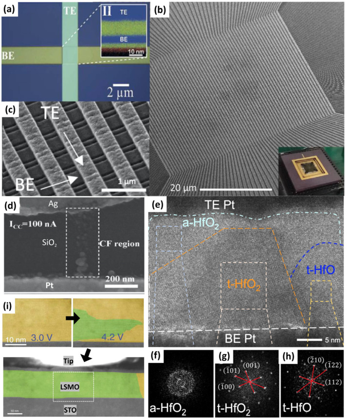 Figure 2
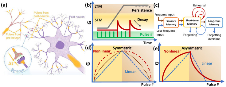 Figure 3
- —MSCA EC
- —Royal Society Research
- —UKRI Engineering and Physical Sciences Research Council
- —Vellore Institute of Technology
Peer Reviews
No public reviews on file for this paper yet. If you reviewed it on a platform where reviews are public (OpenReview, ICLR, NeurIPS, ICML), you can paste yours below so the community can read it here.
Videos
No videos yet. Explain this paper in a talk, walkthrough, or lecture? Add one.
Taxonomy
TopicsAdvanced Memory and Neural Computing · Ferroelectric and Negative Capacitance Devices · Neural Networks and Reservoir Computing
1. Introduction
Currently, the world is becoming increasingly dependent on artificial intelligence (AI) computations. AI-powered chips are not only used for supercomputers and cloud servers but also for personal gadgets and computers, which modern life and the global economy cannot run without. The development of these chips mainly focuses on advanced architectures, e.g., graphic and tensor processing units and AI-specific accelerators, and they stimulate the progress of deep learning due to their high computing speed [1]. Nevertheless, the current computer architecture is based on conventional von Neumann designs that rely on data transfer between the processing unit and memory unit, and its transfer rate is facing a limit as the task complexity increases [2]. This von Neumann bottleneck limits the processing speed due to the shared system bus between the CPU and memory, restricting simultaneous instruction fetching and data processing [3]. This problem makes the AI chips consume high energy and limits their efficiency and scalability [1].
Computing-in-memory (neuromorphic computing) is a new paradigm to solve this problem, where the data do not necessarily have to be processed at the processing unit but at the memory unit itself, mimicking how the human brain works. The brain is the most efficient computing system capable of performing complex data processing, enabled by a large-scale interconnected neural network that stores and processes data at the same place and in parallel [4]. This interconnected neural network is governed by synapses to perform synaptic functions [5].
Several memristive systems, memristor, phase-change, spintronic, and ferroelectric memory devices can mimic the synaptic functions, showing potential for neuromorphic computing architectures; thus, they are called artificial synapses [6,7,8,9,10,11]. Research on neuromorphic computing based on memristive systems has exponentially increased over the last decade, as shown in Figure 1. This trend indicates the urgent demand for faster and smarter computing machines in the real world. Among these memristive systems, it has been shown that phase-change and resistive memories are the most prominent subfields showing rapid growth in development (Figure 1b). However, phase-change memory technology has a long history of scientific contributions, and its development is much more mature [12]. Ferroelectric and spintronic memory devices have been developed over the last few decades [12]. The scientific progress in these fields is not as fast as that in resistive memory. One of the reasons why resistive memory has gained considerable attention is its feasibility for integration with a diode selector, which has the same sandwich structure as a memristor (1D1M, 1-diode 1-memory). In circuit-level implementation, a selected device must be stacked with each memristive system to avoid the sneak-path issue in a massive array configuration. All memristive systems except memristors require transistors as their selectors (1T1M, 1-transistor 1-memory) [13]. The transistor cell structure (10–30F^2^, where F is the feature size) is the constraining factor hindering the fabrication of an ultra-high-density synaptic network, whereas the 1D1M configuration has a cell size of 4F^2^/N (N is the number of stacked layers), which is promising for a large artificial neural network (ANN) [14]. The facile architecture of the two-terminal memristor synapse offers a brain-inspired, highly dense computing element that complies with Moore’s law [2,6,13,15,16,17,18,19,20,21,22].
An ANN employing a 1024-cell array of memristor synapses (memristor-based synaptic devices) consumes much less power than the Intel Xeon Phi processor [6]; von Neumann’s consumes more energy for cognitive learning and data processing, not only because of the CPU memory bottleneck but also because its transistor-based processing unit is volatile and requires continuous power to maintain its synaptic weight [30]. Moreover, ANNs should be integrated with CMOS-based neuron-driving circuits, which are power-hungry [31]. A feasible method to achieve low-power computation is to utilize a low-power ANN based on memristor synapses. The synaptic weight of a memristor synapse can be maintained over a period without continuous power (nonvolatile), and its programming voltage and current are typically 1 V and 10 µA or less, respectively. If typical memristors require 1–3 nJ per spike [32] and 10^8^ spikes are needed for the full 10,000-image MNIST test set (considering about 10^3^ spikes per neuron across 10^4^ neurons firing during training and inference cycles) [33], we can hypothetically estimate that the memristors only consume less than 1 J when scaled to large arrays of memristor devices. On the other hand, if the Xeon Phi processor runs digital CNN-based MNIST and assuming it consumes 225 W under full load, it requires 25 kJ just for one training session [34]. Therefore, the memristors can reduce the overall system-level power consumption by 4 to 5 orders of magnitude [2,35]. Furthermore, the operating power of the memristor synapse can be further reduced by reducing the cell size [36], stacking in a 3D configuration [37,38,39], and insulator and electrode engineering [40,41]. Based on the trend of the energy required to produce synaptic plasticity, shown in Figure 1c, we found that insulator engineering is an effective approach to reduce the power consumption. Nevertheless, memristor synapses have several challenges that hinder their large-scale integration, e.g., device variability, nonlinear and asymmetric weight update, and epoch training variability. This review article discusses these challenges and overviews recent approaches to mitigating them.
2. Architectonics and Device Physics
The basic architecture of a memristor synapse is a two-terminal metal (top electrode)/insulator (switching layer)/metal (bottom electrode) sandwich structure, as shown in Figure 2a. Among various two-terminal configurations, such as planar (both electrodes face each other with a nanometer gap separation) [42], points (the electrodes have crossed [42], circular [28], or rectangular shapes [43], where each cell does not share its electrode(s) with other cells), and crossbars [16]. The crossbar configuration is the most feasible way to achieve a massive ANN because the cells share both the bottom and top electrodes along the intersecting line array, facilitating interconnection between cells (Figure 2b,c).
The synaptic weight of a memristor synapse is controlled by the electrochemistry of the ionic species in the insulator, which drift under the influence of an electric field to build a conduction channel in the switching layer [44]. These ionic species can be cations (metal ions: Ag [45,46,47], Cu [48,49,50], Ni [51], Co [52], In [53,54,55,56], Te [57], or Pd [58]), anions (non-metal ions, oxygen [59], nitrogen [60,61], carbon [62], and their vacancies), or a combination of both (hybrids) [63,64]. Cation-based memristor synapses, also known as conducting-bridge memory or electrochemical metallization memory (ECM), rely on the migration of metallic ions originating from the active electrode (as the cation source) into the switching layer, forming a bridge connecting the bottom and top electrodes. Figure 2d depicts the direct growth of Ag nanobridges in the Ag/SiO_2_/Pt ECM cell [65]. Nevertheless, in some cases, an inert metal may also migrate and form a bridge [66], which could be due to the property of the film affecting the mass transport under an electric field [67]. The geometry of the metallic bridge is governed by film inhomogeneity and electric field distribution, which determine the redox rate, nucleation rate, and ionic mobility of the metal ions. For example, high rates and mobility result in an inverted cone-shaped filament that grows from the inert electrode, whereas low rates and mobility result in discrete nanoclusters growing from the active electrode, forming a forward cone shape [68]. However, if no active electrode is used in the device, the percolation of intrinsic donor defects in the switching film may form a conducting filament because of the drift of anions under an electric field. In metal oxide (MO) and metal nitride (MN) systems, the filament consists of oxygen (V_O_^2+^) and nitride (V_N_^+^) vacancies. The filament is formed by the reduction of oxygen or nitrogen atoms, forming O^2−^ or N^3−^ anions, respectively, where these anions move to the anode and create vacancies (V_O_^2+^ or V_N_^3+^) in the system [69,70]. Other possible ionic vacancy configurations are also possible, depending on the insulator and electrode materials [71,72]. Thereafter, these vacancies are ordered to connect both electrodes as a pathway for electrons to flow from the cathode to the anode.
Several studies have suggested that the arrangement of these vacancies in crystal lattices may induce a phase transformation, forming a highly conducting phase in the switching layer, such as the Zn-dominated ZnO_1−x_ and Ti_4_O_7_ Magnéli phases in ZnO and TiOx systems, respectively; in some cases, it can also induce amorphous-to-crystalline transition to form a conducting filament(s), as depicted in Figure 2e–h [73]. Another piece of compelling evidence for the phase-change phenomenon occurred in the SiO_x_ system, where the filament is in the form of a semi-metallic Si state [74]. A similar phenomenon was also observed in the SrTiO_3_ system; it was found that the formation of Sr-rich secondary phases led to a high current density [59]. It is important to note that no Sr or Ti ionic movement is involved in the switching process. In hybrid-based devices, both anion and cation species are involved in the switching operation, where the filament and bridge coexist to build a complete conduction channel connecting the electrodes [50,75]. Metal cations have a smaller radius and higher mobility than anions; thus, cations may reach the cathode faster, and the bridge structure has a larger portion of the channel than the filament [64]. Nevertheless, the involvement of various species in a complex system, such as memristor synapses with an active metal-doped oxynitride system, requires further investigation to explain the contribution of each defect to channel formation and its impact on synaptic stability.
In contrast to filamentary conduction, an electrochemical reaction can occur in most parts of the bulk switching layer, which is known as a homogeneous or interfacial switching mechanism. This non-filamentary conduction is similar to the anion-based mechanism; in the ZnO-based system, for example, the repulsion of anions (O^2−^) occurs in a much larger region in the bulk, where this process creates a conducting (oxygen-poor) region above the anode and an insulating (oxygen-rich) region below the cathode in the switching layer [76]. In the ABO_3−x_ system, the electrochemical reaction induces a brownmillerite-perovskite phase transformation, a phenomenon known as reversible phase change [77]. Figure 2i depicts the phase transformation process in the LaSrMnO system [78]. Contrary to most metal-oxide systems, the conducting (perovskite) and insulating (brownmillerite) regions in ABO_3−x_ are oxygen-rich and oxygen-poor phases, respectively [79]. Electron transport in LaSrMnO relies on the hopping of electrons via Mn^4+^ and Mn^3+^ cations, and the introduction of oxygen shifts the under-doped phase (insulating) towards the effective doping level, thereby decreasing the electrical resistance [78].
Based on the above discussion, the anion-based filamentary and homogeneous switching behaviors rely on electrochemically induced phase transition. Therefore, we can argue that the physical nature of the filamentary and interfacial mechanism is not simply a pile of oxygen vacancy defects providing electron pathways between the two electrodes; rather, they rely on the transformation of an insulating phase into a conducting phase that occurs in the switching layer.
A similar phenomenon is observed in phase-change memory technologies; however, the difference is that the switching mechanism in phase-change memory relies on a heat-induced phase transition from crystalline to amorphous, which means this process breaks the lattice frames and vice versa [80]. Nevertheless, this similarity brings us to question the fundamental terminology: can we classify anion-based filamentary and homogeneous memristor synapses as a class of (localized) phase-change memory?
A three-terminal structure, known as a memtransistor, was also proposed for fabricating memristor synapses [81]. Unlike the two-terminal memristor synapse, the gate in the memtransistor offers additional control to modify the conduction between the terminals [82]. Although the memtransistor offers operational ability to minimize the sneakpath current across a large-scale array and mitigate device variability [83], the three-terminal device occupies a larger area than the two-terminal crossbar. Thus, this architecture limits high-density 3D integration. Nevertheless, the fabrication flow complexity of the memtransistor architecture is much less than that of any two-terminal memristive synapse with a transistor as the selection device (1T1M).
(a) Typical architecture of two-terminal metal/insulator/metal memristor synapse, adapted from [84] and (b,c) high-density 64 × 64 memristor crossbar array configuration with a total of 4096 memory cells, adapted from [16], (d) cation-based filamentary formations, adapted from [65], (e–h) anion-based filamentary formations observed using TEM, adapted from [73], (i) homogeneous switching was observed using in situ TEM, adapted from [78].
3. Synaptic and Neuromorphic Capabilities
The mammalian brain consists of interconnected neurons that can process complex data via an electrochemical firing mechanism at synapses [85]. Synapses are junctions that connect each neuron in the network, as depicted in Figure 3a, and transfer and receive chemical signals (Ca^2+^, Na^+^, or K^+^ ions, known as neurotransmitters) [86]. Neurotransmission is mediated by the release of glutamate from a presynaptic neuron (the neuron or synapse that sends the neurotransmitter) to a postsynaptic neuron (the neuron that receives the neurotransmitter). Postsynaptic neurons contain AMPA receptors, which influence Ca^2+^ influx, leading to synaptic plasticity [87,88]. Depending on how the presynaptic fires the transmitter and the postsynaptic response towards the incoming signal, the network can exhibit long-term and short-term memorization, which we define as neural plasticity [89,90].
Similarly, the firing mechanism of memristor synapses was achieved using electrical pulses, and the synaptic response was measured in terms of conductivity, as shown in Figure 3b. In this case, the cathode acts as the pre-synapse and the anode as the post-synapse, whereas the mobile cation/anion in the insulator layer acts as the transmitter (Figure 2). Various pulse schemes can be used to program memorization (synaptic strength); typically, a slow rate and low-amplitude stimulus will result in short-term memory (STM) that can retain the response for a short period (sub-milliseconds to minutes), after which the device starts to forget, followed by a rapid decay of conductance, as illustrated in Figure 3c [91].
(a) Schematic of synapses, reprinted from [92]; (b,c) short-term and long-term memory effect on memristor synapse with different forgetting behavior, inspired by [89]; (d,e) symmetric and asymmetric synaptic feedback exhibiting linear and nonlinear actuation.
STM can evolve into long-term memory (LTM, hours to days) upon high-frequency stimuli or vice versa via opposite amplitudes. The rehearsal and forgetting mechanisms are similar to how the brain learns and processes information [87,88]. The decay rate of synaptic weight can be natural (intrinsic decay), programmed, or a combination of both. The increase and decrease in synaptic weight are called potentiation and depression processes, respectively, and the a/symmetricity of the potentiation and depression can be a linear or nonlinear response, as depicted in Figure 3d,e. Ionic or organic-based memristor synapses often exhibit symmetric feedback, but these types of devices are less stable for lifelong deployment; meanwhile, metal oxide-based devices are more durable but have asymmetric feedback because of the physical nature of the growth and dissolution of the conduction channel in the oxide [93]. Symmetrical synaptic feedback offers a more straightforward computing algorithm at the system level, and it is suggested that linearity determines the computing accuracy [94]. Most metal-oxide memristor synapses require soft breakdown (electroforming) to activate synaptic feedback (Figure 4a) [16]. Different pulse schemes produce different synaptic feedback; Figure 4b–f show the typical identical pulse (pairs) and nonidentical pulse schemes, and the nonidentical pulse often offers better linearity than its identical counterpart [2,16,17]. Linearity can also be enhanced by material and interface engineering [2,16]; it is suggested that a multilayer switching film is an effective method to improve the linearity, since each layer has unique nanostructure and defect properties; thus, controlling the filament or bridge configuration during the synaptic process becomes easier [95,96]. However, there is still less research on the impact of nonlinear and asymmetric feedback on the speed and accuracy of ANN computations in actual implementation.
Besides nonlinearity, temporal variation, such as conductance drift and the dynamic range disparity, which often occur due to cycle-to-cycle and device-to-device fluctuation, can significantly affect the learning accuracy of the network. It is suggested that a network with a temporal variation of more than 22% would not be able to achieve 90% learning accuracy [97]. Device stacking techniques have been proposed to mitigate the temporal variation, e.g., 2M1T (a series of two memristor synapses connected with a transistor) [98], or place several memristors in parallel to suppress the random rejuvenation of the filament during the synaptic training process [99].
Optical illumination can also induce or facilitate synaptic responses. Ref. [100] reported the optical stimulation of a BP-based memtransistor using 280 nm and 365 nm UV light for potentiation and depression, respectively, as shown in Figure 5a,b. The pulse width of the light stimuli can be adjusted to tune the linearity (Figure 5c,d). Yan et al. [101] suggested that light stimuli trigger charge trapping and release mechanisms in the CsPbBr_2_ synapse (Figure 5e–h). A similar mechanism can be found in the two-terminal planar Graphene/MoS_2_ memristor synapse, where the light pulses induce photogenerated trapped electrons, thus enabling programming and erasing functions in the device (Figure 5i–k) [102]. Metal oxide-based memristor synapses with point configurations can also produce photo-induced synaptic behavior, suggesting that the mechanism behind the increase or decrease in synaptic weight during light stimulation is due to the ionization and neutralization of oxygen vacancies in the oxide layer, respectively [103]. These devices require transparent electrodes, such as indium tin oxide (ITO), or a thin metal layer to enable light to penetrate the electrode into the oxide layer. It was found that various wavelengths, from ultraviolet to visible to infrared, can induce a photosynaptic response. Note that ultraviolet light is most commonly used to trigger the photosynaptic response owing to its high energy. Nevertheless, further investigations should be conducted to clarify or confirm the mechanism behind the photosynaptic response in devices with ITO electrodes. The high absorption of ITO in the UV region absorbs light before it can be transmitted into the oxides; thus, this brings us another idea that we may not necessarily expose the insulator layer if we can employ photosensitive electrode materials.
Table 1 summarizes the performance metric of optomemristor and optomemtransistor synapses. Both the optomemristor and optomemtransistor are suitable for visual AI systems due to their acceptable optical speed. Even though optomemtransistor synapses could perform with better accuracy in conductance modulation and fast photoresponse and high responsivity, their engineering complexity and integration may result in a higher fabrication cost than that of optomemristors. The use of perovskite or 2-dimensional materials tends to lead to a better optical performance [104]. However, these materials are often sensitive to ambient aspects, e.g., temperature and humidity, that can pose challenges for practical use [105,106,107]. Table 2 summarizes common problems in developing 2-dimensional memristor synapses. A careful and tedious synthesis route is required to grow these materials, and slight process variation in the nanostructure or defect configuration could significantly affect their characteristics and performance.
Remembering and forgetting are neuronal functions that neuromorphic computing systems try to mimic [121] and are deeply rooted in the learning rules that are used to modulate synaptic weights. A neurophysiologist, Donald Hebb, proposed that synaptic weight changes in biological neural networks may vary depending on the time gap between spikes, known as Hebbian learning rules (HLRs) [122], the most common of which are shown in Figure 6a. Spike timing-dependent plasticity (STDP) and spike rate-dependent plasticity (SRDP) are frequently used as programming algorithms for implementing these rules [123]. STDP works on the relative timing between the pre- and postsynaptic spikes and influences the magnitude and direction of the weight update [124], whereas SRDP works on synaptic weight modulation by controlling the frequency of spiking neurons in the neural network, as illustrated in Figure 6b. Although STDP is mostly reported in memristor synapse development owing to its practical implementation in decreasing or increasing the weight with precise timing of each spike, SRDP is closer to biological neuronal functions, where the spike rates control synaptic strength (Figure 6c). Peng et al. [125] suggested that the SRDP is an efficient algorithm for high-accuracy unsupervised online learning. Ideally, a memristor synapse should be able to perform HLRs. Yi Li et al. [126] reported that a Ge_2_Sb_2_Te_5_-based memristor synapse can exhibit all four rules with fast response time and low-power operation. However, most memristor synapse designs in the literature fail to demonstrate HRLs.
4. Hardware Implementation and Future Scope
Recent advancements in memristor-based neuromorphic systems have enabled a wide spectrum of biomedical applications. These can be broadly categorized based on the nature of the signal they process—optical signals for vision restoration, electrochemical signals for organ-level implants, and electrophysiological signals for wearable health monitoring. Additionally, these applications vary in their level of invasiveness, ranging from fully implantable devices to non-invasive wearable electronics. This section explores these applications in a structured manner to highlight the synergy between device-level innovations and system-level healthcare solutions.
4.1. Optical Signal Processing: Artificial Retinas and Vision Systems
Li et al. [128] proposed a VO_2_-based ultraviolet nonvolatile synapse memtransistor actuated by 650, 532, 450, and 375 nm light sources. The synapse response of the memtransistor was used for neural network simulation to recognize handwritten numbers from the MNIST dataset. Figure 7a depicts the single-layer feedforward artificial neural network with 784 neuron input layers, 300 neuron hidden layers, and 10 neuron output layers presented in this network. The neural network was trained using the original MNIST test dataset, the RGB Gaussian noise dataset, and preprocessed data. The neural network recognition accuracy was simulated as shown in Figure 7b. The preprocessed dataset and the original MNIST test dataset achieved a recognition accuracy of 93%, whereas the dataset with RGB Gaussian noise achieved only 24% accuracy. The hardware implementation of a multilayer perceptron (MLP) neural network was realized by Bayat et al. by developing a 20 × 20 memristor synapse crossbar array based on Pt/Al_2_O_3_/TiO_2−x_/Ti/Pt. The MLP consists of 16 input neurons, 10 hidden layer neurons, and 4 output neurons. The hardware-based neuron network was trained to classify 4 × 4 pixel patterns, shown in Figure 7c. MNIST simulations based on memristor synapses typically achieve 90–95% accuracy; this performance is close to the accuracy achieved by traditional ANN software-based or other hardware, which could achieve up to 99% [129,130,131].
In recent years, implantable electronics has grown rapidly owing to the significant leaps achieved by various artificial vision projects worldwide [133,134]. An artificial cognitive retina is based on a biocompatible synaptic array, such as a retinal implant, to transmit images efficiently into an optical neuronal signal. Retinal implants are directly connected to the optic nerve in the human brain. The main function of optical nerves in humans is to transmit visual data obtained from the rod and cone cells of the retina to neuronal signals of the human brain, which are then processed by the human brain as visual signals. Figure 8a depicts the location of the retinal implant connecting the optical nerves and retina [135]. The image from the camera was processed using a 3D stacked memristor array, which was then transferred to the retinal implant, as shown in Figure 8b,c. The 3D stacked crossbar memristor that processes the image data into optical nerves as a visual impulse. The artificial neural network comprises two hidden-layer biocompatible synaptic memristor arrays for converting electronic data (image data) to chemical translation (optical nerves). The structure of the neural network is shown in Figure 8d. The first layer of this neural network array was employed to capture a visual image and imprint it into an array of artificial neural networks.
The successive layer participates in the computations to further conduct the image processing operation for conversion into an optical signal. The primary function of the optical nerves is to convert images into signals. Retinal implants are expected to help improve the lives of patients with visual disabilities. Seo et al. proposed an artificial optic-neural synapse [136] that contributes to a significant enhancement in synthetic vision by directly interfacing an optical sensing device with a synaptic device connected to the visual cortex of the human brain. The structure of the integrated h-BN/WSe_2_ (optical sensing) and WSe_2_-based (synaptic device) is shown in Figure 8e. The schematic also illustrates a symbolic representation of the connected device used in the study. The synaptic device is expected to be integrated into an array of neural networks for high-density integration and realization of artificial vision. The synaptic device response can be used in an optical neural network of RGB-based synaptic devices, and the neural network can achieve a peak recognition rate that exceeds 90% Figure 8f,g. While optical signal processing is crucial for restoring vision, similar neuromorphic architectures can be adapted for electrochemical interfaces in vital organ implants. These systems enable real-time monitoring and data interpretation directly within the body.
4.2. Electrochemical Interfaces: Organ-Level Implants
In the future, memristive HNN cannot be restricted to bionic vision in the healthcare sector. HNN can be utilized in various applications, including heart, brain, ovarian, and lung implants, which are integrated with HNN, as depicted in Figure 8h,i. Artificial neural networks could dominate the future of biomedical applications, from heart implants to human brain implants. The future of biomedical analysis can be carried out using heart or brain implants with sensors and an HNN to harness the data processing of the functionality of human organs. The HNN can also categorize patients’ diseases using the data available from implants. Memristor synapses leveraging electrochemical interfaces are groundbreaking for organ-level implants, as they mimic biological synaptic function through ionic and redox-driven resistance switching, thus enabling ultra-low-power and scalable architectures for physiological data processing [138]. Hardware neural networks incorporating memristor crossbar arrays can process multichannel physiological signals from these implants by applying learning algorithms like spike-timing and rate-dependent plasticity, supporting responsive closed-loop interventions directly at the organ interface. Implanting memristor synapses on the heart could facilitate real-time, energy-efficient detection of irregular cardiac activity by encoding and evaluating biosignals locally [139]. For brain implants, memristor synapses allow high-fidelity neural recording and the adaptive neuromodulation necessary for cognitive rehabilitation, via robust hardware neural network architectures; similarly, ovarian implants can exploit memristor synapses for continuous hormonal cycle monitoring, supporting both diagnosis and therapy through on-site computation with minimal energy overhead [140]. Another successful proof-of-hypothesis has also been reported for applications in functional monitoring of blood supply during liver transplantation [141]. This enables implantable electronics to perform real-time classification, anomaly detection, and feedback using integrated neuromorphic architectures proven to work in biomedical scenarios [142]. Beyond invasive implants, neuromorphic computing also supports non-invasive health monitoring through wearable electronics. These devices serve as external hubs, collecting and analyzing electrophysiological signals to provide continuous health insights.
4.3. Electrophysiological Monitoring: Wearable Sensors
Memristor synapses are revolutionizing non-invasive health monitoring through their potential integration into wearable electronics for ECG, SpO_2_, heart rate, and blood pressure measurement [137]. Memristors can act as external hubs, continuously collecting electrophysiological signals and leveraging neuromorphic architectures for low-latency data processing [143]. The use of memristor-based in-memory computing within these wearables allows real-time analysis and pattern recognition directly at the sensor level, which is essential for anomaly detection such as arrhythmias or abnormal blood oxygenation [144]. By embedding computational functions into the storage medium, memristor synapses minimize energy consumption, enable scalable data fusion, and facilitate instant feedback to healthcare providers or end-users, ensuring timely intervention and improved patient outcomes [145]. Wearable electronics, which could act as a data hub to connect these implants, demonstrate the live functionality of the human organs and display the data using transparent electronic eyeglasses or notify doctors. By using a similar approach, Ni et al. [146] proposed FeFET-based sensor data fusion technology using in-memory or neuromorphic memory computing. The FeFET-based neural network was designed to detect anomalies in the live ECG, SpO_2_, heart rate, and blood pressure of human physiological signals. An in-memory logical array was designed to monitor and analyze human physiological signals. The in-memory correlation detection array is composed of multiple sensors that feed input to the correlation detection system, which is composed of a neural network of processing in the FeFET, and the anomaly detection scheme is used to detect anomalies in physiological signals.
5. Conclusions
Resistive-synapse-based neuromorphic computing offers great potential for the development of next-generation AI hardware. The mimicking property of memristor synapses allows for the emulation of cognitive activity similar to that of the human brain, which exhibits STDP and SRDP. Research on highly dense crossbar array-based HNNs shows a significant leap by realizing a simple perceptron neural network proposed to perform various applications based on recognition, classification, and detection. In the future, we anticipate that HNN-based systems will be used for broad healthcare solutions, including artificial vision, EEG signal monitoring, vital organ implants, disease detection, and physiological signal monitoring. Nevertheless, system-oriented benchmarking for memristor synapses should be developed to determine the minimum required synaptic performance for certain applications to ensure better synergy and a scientific leap between cleanroom engineers (device level) and system designers (system level). We also foresee further scientific progress in memristor synapses that mimic various types of neurons by controlling defects to behave like biological neurotransmitters. Therefore, the development of the next generation of memristor synapses will extend beyond elemental-to-molecular-level neural networks with massive interconnections close to the human brain.
The reference list from the paper itself. Each links out to its DOI / PubMed record.
- 1Hou W. Exploring the Horizon of AI Development: Navigating Constraints of Chips and Power in the Technological Landscape Appl. Comput. Eng.20247717718210.54254/2755-2721/77/20240688 · doi ↗
- 2Yu S. Neuro-Inspired Computing with Emerging Nonvolatile Memory Proc. IEEE 201810626028510.1109/JPROC.2018.2790840 · doi ↗
- 3Syed G.S. Le Gallo M. Sebastian A. Non von Neumann Computing Concepts Phase Change Materials-Based Photonic Computing Elsevier Amsterdam, The Netherlands 20241135
- 4Dittmann R. Strachan J.P. Redox-Based Memristive Devices for New Computing Paradigm APL Mater.2019711090310.1063/1.5129101 · doi ↗
- 5Zidan M.A. Strachan J.P. Lu W.D. The Future of Electronics Based on Memristive Systems Nat. Electron.20181222910.1038/s 41928-017-0006-8 · doi ↗
- 6Yao P. Wu H. Gao B. Eryilmaz S.B. Huang X. Zhang W. Zhang Q. Deng N. Shi L. Wong H.-S.P. Face Classification Using Electronic Synapses Nat. Commun.201781519910.1038/ncomms 1519928497781 PMC 5437298 · doi ↗ · pubmed ↗
- 7Wu W. Wu H. Gao B. Deng N. Yu S. Qian H. Improving Analog Switching in Hf Ox-Based Resistive Memory with a Thermal Enhanced Layer IEEE Electron. Device Lett.2017381019102210.1109/LED.2017.2719161 · doi ↗
- 8Suri M. Bichler O. Querlioz D. Cueto O. Perniola L. Sousa V. Vuillaume D. Gamrat C. De Salvo B. Phase Change Memory as Synapse for Ultra-Dense Neuromorphic Systems: Application to Complex Visual Pattern Extraction Proceedings of the Technical Digest—International Electron Devices Meeting, IEDM 2011 Washington, DC, USA 5–7 December 20114.4.14.4.410.1109/IEDM.2011.6131488 · doi ↗