Near-commensuration from Intertwined Charge Density Waves in Single-Layer TiSe2
Wen Wan, Maria N. Gastiasoro, Daniel Muñoz-Segovia, Paul Dreher, Miguel M. Ugeda, Fernando de Juan

TL;DR
Researchers observed a new near-commensurate state in TiSe2, revealing complex interactions between charge density waves and nematicity.
Contribution
The study identifies a novel near-commensurate state in TiSe2 involving intertwined charge density waves and nematicity.
Findings
A near-commensurate state in TiSe2 is revealed with unidirectional domain walls.
The state involves two coupled real charge density waves of different symmetry.
An unexpected nematic modulation is coupled to the charge density waves.
Abstract
When the period of an incommensurate charge density wave (ICDW) approaches a multiple of a lattice vector, the energy gain from locking the period can drive a transition into an intermediate near-commensurate (NC) state made of locally commensurate regions separated by phase slips of a complex CDW. In TiSe2, a paradigmatic CDW system, incommensuration is believed to be induced by carrier doping, yet its putative NC state has never been imaged. Here we observe a striking NC state in ultraclean, doped monolayers of TiSe2, displaying an intricate network of unidirectional domain walls. Detailed analysis reveals that these are not phase slips of a complex CDW, but rather sign-changing Ising-type domain walls of two coupled real CDWs of different symmetry. In addition, these CDWs are coupled to an unexpected nematic modulation at the lattice Bragg peaks. TiSe2 is thus a rare example of a…
Genes, proteins, chemicals, diseases, species, mutations and cell lines named across the full text — each resolved to its canonical identifier and authoritative record.
Click any figure to enlarge with its caption.
 2
2 3
3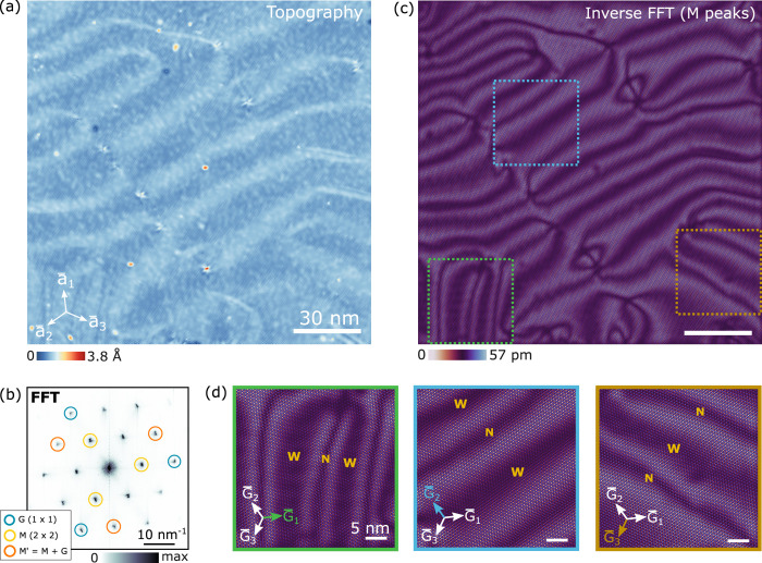 4
4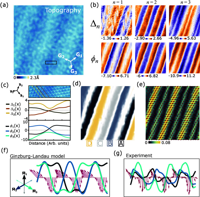 5
5- —European Commission10.13039/100010663
- —Ministerio de Ciencia, Innovaci??n y Universidades10.13039/100014440
- —Ministerio de Econom??a y Competitividad10.13039/501100011033
- —Ministerio de Econom??a y Competitividad10.13039/501100011033
- —Ministerio de Econom??a y Competitividad10.13039/501100011033
- —Ministerio de Econom??a y Competitividad10.13039/501100011033
Peer Reviews
No public reviews on file for this paper yet. If you reviewed it on a platform where reviews are public (OpenReview, ICLR, NeurIPS, ICML), you can paste yours below so the community can read it here.
Videos
No videos yet. Explain this paper in a talk, walkthrough, or lecture? Add one.
Taxonomy
Topics2D Materials and Applications · Organic and Molecular Conductors Research · Topological Materials and Phenomena
Understanding how incommensurate charge density wave (ICDW) states lock to the crystal lattice in an incommensurate to commensurate (I–C) transition is a fascinating problem with profound implications on how other ordered states such as superconductivity emerge in their presence.? Due to the energetics of lattice locking, the I–C transition typically proceeds via an intermediate near-commensurate (NC) phase characterized by locally commensurate domains separated by domain walls (see phase diagram in Figureb). The nature of these domain walls and of the I–C transition itself depends on whether the CDW order parameter is real or complex, which is determined by the commensurate CDW (CCDW) period.? In a one-dimensional (1D) CCDW with wavevector and lattice constant a, lattice translations for N > 2 are represented by a phase factor e^ i2π/N ^ and the order parameter is complex. In this case, the NC state has approximately constant amplitude but shows regions of constant phase separated by phase slips known as discommensurations,? akin to domain walls of easy-plane ferromagnets. If the CCDW has period N = 2 however, translations are represented by a sign change (e^ i2π/N ^ = −1) and the order parameter is real. In this case, only real sign-changing domain walls where the order parameter goes through zero are possible, akin to domain walls in Ising ferromagnets (see SI).
TiSe_2_ (Figurea) is a paradigmatic example of one such N = 2 triple-Q CDW, which can be driven through a C–I transition by electronic doping. The bulk CDW wavevector is and Cu doping? or applying pressure? leads to an out-of-plane incommensurate CDW state which becomes superconducting at T C ∼ 2–4 K.? In-plane incommensuration is not resolved in X-rays, but STM studies in Cu- and Pt-doped samples do observe in-plane CDW domain walls ?−? ? ? ? with a disordered spatial distribution likely dominated by CDW pinning by the Cu dopants, and indirect transport signatures of incommensuration were reported in gated thin films.? Direct evidence of an NC state, i.e., a long-range ordered array of in-plane domain walls, remains lacking as this would require imaging a homogeneously doped sample without disorder. To disentangle the more complex out-of-plane incommensuration, this should ideally be done in the single-layer limit, where the N = 2 CDW remains essentially unchanged from the bulk. ?−? ? ? ? ? ?
In this Letter, we demonstrate that a doped monolayer of TiSe_2_ exhibits an intrinsic in-plane NCCDW state with a wavelength of 20 nm, which remains coherent over hundreds of nanometers. We uncover the spatial structure of the NC state via high-resolution STM measurements combined with standard phase-locking techniques and show that it is made of a train of intertwined Ising domain walls of two independent order parameters with opposite mirror parity, shown schematically in Figurec. These domain walls concatenate four CDW domains out of the eight available ones (A through D′ in Figured) in a periodic arrangement. Our analysis also reveals the existence of a strong nematic modulation of the lattice coupled to the domain wall train. This complex NC state is naturally accounted for by Ginzburg–Landau theory, including the order and number of the domains and their coupling. Our work clearly shows how TiSe_2_ proceeds through the doping-driven C–I phase transition via a NC state of Ising domains.
Extracting CDW Order Parameters
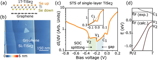
Our experiments were carried out on a nearly full monolayer of 1T-TiSe_2_ grown on epitaxial bilayer graphene (BLG), as sketched in Figurea. Our samples display remarkable uniformity with single-crystal domains several hundreds of nanometers in size (Figureb) and a density of point defects below 1 × 10^12^ cm^–2^. A typical STM dI/dV spectrum, showing the low-lying electronic structure of single-layer TiSe_2_, is shown in Figurec (for a larger energy range, see SI). Three step-like features for occupied states are observed at V s = −215 ± 5 mV (labeled V 1), V s = −365 ± 5 mV (labeled V 2), and a subtler step with opposite orientation (see inset) labeled C 1 is observed at V s = −65 ± 5 mV. These features match the band structure of monolayer TiSe_2_ in the CDW phase,? which shows an electron band of Ti-3d character (back-folded from M⃗ _ n ) and two spin–orbit split Se-4p hole bands (E SOC = 150 ± 10 meV) (Figured) separated by the CDW gap (E G = 150 ± 10 meV). ?−? ? ? ? ? This identification is also supported by previous angle-resolved photoemission spectroscopy (ARPES) measurements,? which revealed a small electron doping because the d-electron band is partially filled. This likely originates from charge transfer from the substrate, as demonstrated recently by comparing TiSe_2 monolayers grown on different substrates.?
(a) Side-view sketch of monolayer TiSe2 on graphene. (b) Large-scale STM image of nearly one layer of TiSe2 on BLG/SiC(0001) (V s = 2.4 V, I t = 15 pA). (c) Typical STM dI/dV spectrum acquired on monolayer TiSe2/BLG showing electronic features V 1, V 2, and C 1 (I t = 2 nA). The colored shadows below the curve indicate the SOC splitting (green) and the gap (blue). Inset shows a zoom around the C 1 feature. (d) Calculated band structure of the isolated monolayer TiSe2 in the CDW 2 × 2 phase (adapted from Chen et al., ref , licensed under CC BY 4.0). The position of the experimental E F is also indicated.
Our atomically resolved STM images of the CDW state show the expected 2 × 2 order at small scales (Figurea), where the CDW unit cell (white hexagon) is doubled in both lattice directions compared to the crystal unit cell (green hexagon). The corresponding Fast Fourier transform (FFT) in Figureb shows clear superlattice Bragg peaks at both Q⃗ _ n _= M⃗ _ n _ = G⃗ _ n /2 (n = 1, 2, 3) and the higher harmonic M⃗ _ n _ ^′^ = M⃗ _ n _ + G⃗ _ n–1 (yellow and orange circles, respectively), which are the signature of 2 × 2 order. While this modulation seen in STM has traditionally been identified ?−? ? ? ?,?−? ? ? as resulting from the 2 × 2 lattice distortion observed in neutron scattering,? we now show that the STM modulation actually reflects the existence of two CDW order parameters of different symmetry.
*(a) Atomically resolved STM image of monolayer TiSe2 in the CDW state showing the 2 × 2 reconstruction (V s = 0.1 V, I t = 1.5 nA). The atomic and CDW unit cells are indicated in green and white, respectively. (b) FFT of the STM image in panel a, showing CDW Bragg peaks at M⃗
n and M⃗
n
′. (c) Modulus κ=13∑n(ϕnα)2 for α = Se-Up, Ti, Se-Down (upper plot) and extracted order parameters Δ n (x) and ϕ n (x) ≡ ϕ n
SeUp(x) from the CDW peak (lower plot) plotted along the dashed white line in the zoomed-in region shown above. (d) Real-space contour plot of ρ(x⃗) reconstructed by taking averaged values of the order parameters in panel c showing the slightly counterclockwise rotated propeller when Δ1Δ2Δ3 < 0.*
The primary CDW order parameter of monolayer TiSe_2_ (point group symmetry D _3d ) is a transverse phonon of symmetry M 1 ^–^ ? (irrep A _ u _ of the little group C 2h _ at M), which is odd under both inversion and the mirror plane σ v _ parallel to the corresponding M⃗ _ n _ vector. A depiction of the triple-Q M 1 ^–^ phonon distortion is shown in Figurec, with in-plane black arrows representing the displacements of the top Se layer. These displacements give rise to a rotated propeller-like motif commonly observed in STM experiments, represented in purple in the figure. A secondary CDW order parameter of M 1 ^+^ symmetry, representing a modulation where one out of four Se atoms rises upward, is symmetry allowed and condenses simultaneously at the CDW transition.? The corresponding M 1 ^+^ distortion, even under both inversion and mirror σ v _, is also depicted in Figurec (out-of-plane black arrows). Note that in the monolayer, an M 1 ^–^ distortion generically makes the ground state chiral,? unlike in the bulk where L 1 ^–^ always preserves an inversion center between layers.
In our monolayer samples, the M 1 ^–^ and M 1 ^+^ modulations can be distinguished in STM by their mirror parity as follows. The charge density in the CDW state is approximately given by ρ(x) = 2Re[∑_ n _ A _ n _ ^ G ^ e^ iG⃗ _ n _ x⃗ ^ + A _ n _ ^ M ^ e^ iM⃗ _ n _ x⃗ ^ + A _ n _ ^ M ^′^ ^ e^ iM⃗ _ n _ ^′^ x⃗ ^], where A _ n _ ^ q ^ are complex numbers at the q⃗ = G⃗ _ n , M⃗ _ n , and M⃗ _ n _ ^′^ FFT peaks. Because lattice translations act as real numbers e^ iq⃗ _ i _ a⃗ ^ = ±1 for any q⃗ _ i , the real and imaginary parts of A _ n _ ^ q ^ encode independent 2 × 2 modulations, which may even have different symmetry. Since M⃗ _ n _ (M⃗ _ n _ ^′^) is parallel (perpendicular) to σ v , the modulation e^ iM⃗ _ n _ x⃗ ^ is invariant under σ v , while for M⃗ _ n _ ^′^, e^ iM⃗ _ n _ ^′^ x⃗ ^ → e^–iM⃗ _ n _ ^′^ x⃗ ^. This implies that ReA _ n _ ^ M ^, ImA _ n _ ^ M ^ and ReA _ n _ ^ M ^′^ ^ all represent mirror even 2 × 2 modulations, while only ImA _ n _ ^ M ^′^ ^ represents a mirror odd 2 × 2 modulation. Hence, the primary CDW order parameter, which we call Δ n , can only be Δ n _ = ImA _ n _ ^ M ^′^ ^, which is sensitive to the small in-plane modulations of the Se atoms of symmetry M 1 ^–^. The other three mirror even signals (ReA _ n _ ^ M ^, ImA _ n _ ^ M ^, ReA _ n _ ^ M ^′^ ^) can be rearranged into three M 1 ^+^ order parameters ϕ n _ ^α^ showing the 1-in-4 pattern localized at the upper Se (ϕ n _ ^SeUp^), Ti (ϕ_ n _ ^Ti^), and lower Se (ϕ_ n _ ^SeDo^) sites, respectively (Figurea; See SI).
To extract all these order parameters, we implemented the Lawler–Fujita? (LF) algorithm to produce corrected images in a perfect registry with the lattice, which allows extraction of the complex numbers A _ n _ ^ M ^ and A _ n _ ^ M ^′^ ^ with well-defined phases (see SI). Figurec shows a 1D cut of the extracted M 1 ^+^ secondary order parameters ϕ_ n _ ^SeUp^, ϕ_ n _ ^Ti^, and ϕ_ n _ ^SeDo^, showing the dominance of ϕ_ n _ ^SeUp^ as this layer is the closest to the STM tip. Because of this, from now on, we only consider ϕ_ n _ ≡ ϕ_ n _ ^SeUp^ as the secondary CDW order parameter. The extracted primary and secondary order parameters, Δ_ n _ and ϕ_ n _, along the same 1D cut are also shown in Figurec, revealing finite n = 1, 2, 3 components of the triple-Q CDW state.
As a check, in Figured we reconstruct an approximate ρ(x) from the spatially averaged order parameters obtained from Figurec (see SI). In remarkable agreement with the original image (Figurea), Figured shows the same weakly rotated propeller-like shape and the 1-in-4 bright feature of the Se atoms. The rotation of this propeller reflects the existence of Δ_ n , with its chirality (clockwise vs counterclockwise) given by the sign of Δ_1_Δ_2_Δ_3, while the 1-in-4 bright upper Se atom originates from ϕ_ n . The four choices in the CDW unit cell for the propeller center, determined by the signs of Δ n _ and ϕ_ n , make eight possible CCDW ground states, which we label A, B, C, D for one chirality and A′, B′, C′, D′ for the other (represented in Figured) and Figurec corresponds to state A. A faithful extraction of the primary Δ n _ and secondary ϕ_ n _ order parameters, performed for the first time here, is crucial to understand the symmetry and domain structure of the CDW, including in incommensurate states.
Near-commensurate CDW State
Our main experimental result is now revealed by our high-resolution topography images taken over very large scales, which show a highly inhomogeneous 2 × 2 CDW displaying a striking long-range ordering of domains characteristic of a near-commensurate phase. Figurea shows an atomically resolved STM image of 153 nm × 153 nm in size, where long striped regions dominate the topography, forming an intricate pattern. The FFT of this image (Figureb) reveals characteristic CDW peaks at M⃗ _ n _ and M⃗ _ n _ ^′^ as observed for a single domain (Figureb). While correcting the phase drift with the LF algorithm in such a large image is not possible, the Fourier-filtered amplitude (insensitive to phase drift) of the M⃗ _ n _ peaks (Figurec), reveals that the long-wavelength topography modulation indeed comes from a modulation of the CDW and shows that the wavelength appears halved compared to the topography. We systematically observed these patterns in tens of different regions in several TiSe_2_/BLG samples (see SI), enabling us to extract an averaged periodicity of λ = 20 ± 2 nm for the modulation induced perpendicular to the domain walls. Remarkably, the incommensuration is single-q in character (i.e., the modulation produces 1D stripes and is not a 2D network as previously believed). ?,? The 1D trains of domains in Figurec form “superdomains” that can be distinguished by the modulation vector q⃗ NC, roughly parallel to one of the CDW wavevectors Q⃗ _ n _. A zoom of the three types of superdomains (Figured) reveals a finer feature of domain walls: two classes of them, wide and narrow, alternate within the superdomain train.
*Near-commensurate CDW state. (a) Atomically resolved STM topography of a 153 nm × 153 nm region (V s = −0.05 V, I t = 60 pA). Lattice vectors are shown as white arrows. (b) FFT image of panel a. (c) Inverse FFT of the amplitude of the CDW M⃗
n peaks from panel b (see SI for M⃗
n
′). A network of 1D trains of domains (high amplitude) separated by domain walls (low amplitude) with an average spacing of 20 nm is observed. (d) Zoom-in of three regions shown in colored squares in panel c, showing that domain walls are approximately perpendicular to G⃗
n and alternate between wide (W) and narrow (N) types.*
The behavior of the CDW in the single-layer limit sharply contrasts both with pristine bulk TiSe_2_, where the CDW shows a commensurate, single-domain phase, ?,? and with bulk doped samples, which show short-range, disordered domain walls. ?−? ? ? ? The ordered domain structure in the single layer cannot be attributed to disorder given the low density of defects of our films (see SI) and instead represents an intrinsic near-commensurate state. These patterns can still be seen at 77 K but are not present above T CDW ≈ 230 K, as seen in our STM images at room temperature (see SI), which also ensures that they are not extrinsic and originate from the CDW incommensuration.
Intertwined CDW order parameters
To analyze the order parameter structure of the NC state, we selected an STM image with a single superdomain (Figurea) where q⃗ NC ∝ G⃗ 2. The extracted order parameters are shown in Figureb, which reveals another striking feature: the modulation of the three Δ_ n _ components is different, approximately following Δ_2_ ∝ sin(2q⃗ NC x⃗), Δ_1_ ∝ sin(q⃗ NC q⃗) + c sin(3q⃗ NC x⃗), and Δ_3_ ∝ cos(q⃗ NC x⃗) – c cos(3q⃗ NC x⃗) with |c| <
- The secondary order parameter components follow a similar pattern with the opposite sign, ϕ_ n _ = −Δ_ n . This leads to sign alternation of domains which produces the pattern “ABCD” illustrated in Figured, concatenating the four CCDW states with counterclockwise chirality Δ_1_Δ_2_Δ_3 < 0 (left column in Figured). A zoom around a domain wall in Figurec shows how a given pattern of sign changes shifts the center of the CDW by one atomic unit cell: in this case, the transition from state B to C corresponds to a translation by lattice vector a⃗ 3.
Ising domains of intertwined CDW order parameters. (a) High-resolution topograph of a superdomain with q⃗ NC ∝ G⃗ 2 after LF correction (V s = −0.05 V, I t = 40 pA). (b) Extracted order parameters, ϕ n (x⃗) and Δ n (x⃗). Note that Δ2 oscillates twice as fast as Δ1,3 and ϕ n ∼ −Δ n . (c) Close-up of a domain wall in the STM image in panel a (black box) and corresponding 1D cuts of the order parameters. The domain wall connects state C (left) to B (right), according to the convention in Figure d. This corresponds to a real space shift by a⃗ 3 (illustrated by dashed lines). (d) Color map of domains extracted from panel b, which shows the train ABCD. (e) Nematicity map N⃗(x⃗) obtained from the lattice Bragg peaks (color maps |N⃗(x⃗)| and the arrows indicate its direction). N⃗(x⃗) lives on domain walls and alternates its direction between G⃗ 1 (wide domain walls) and G⃗ 3 (narrow domain walls). (f, g) A 1D cut of ϕ n (q⃗ NC x⃗) (full lines) and N⃗(q⃗ NC x⃗) (red arrows) (f) from the GL theory and (g) from the STM experiment.
The LF analysis also reveals a very strong modulation of the imaginary lattice Bragg peaks ImA _ n _ ^ G ^, while ReA _ n _ ^ G ^ remains smoother. To track this modulation, we define a nematic order parameter
that vanishes above T CDW and selects a preferred axis as the CDW sets in. Figuree shows its intensity and direction dependence across the single superdomain. Intriguingly, this nematicity is strongest in the domain walls, where the CDW is weakest. Furthermore, it points along G⃗ 1 for wide domain walls and along G⃗ 3 for narrow ones, showing it is strongly coupled to the CDW modulation.
The observed domain wall phenomenology can be understood from the Ginzburg–Landau (GL) theory of coupled CDW order parameters Δ_ n _ and ϕ_ n _, whose energy density is . The first term governs the CCDW phase
where for order parameters ϑ = Δ,ϕ, and we have only included a single quartic term for simplicity. Finite primary Δ_ n _ develop when a Δ < 0, which leads to finite secondary ϕ_ n _ through a finite b Δϕ. Because ϕ_ n _ is mirror even, a cubic term b ϕ is allowed; this coefficient selects the sign of ϕ_1_ϕ_2_ϕ_3_. Indeed, we have experimentally observed only domains where ϕ_1_ϕ_2_ϕ_3_ > 0 that fixes b ϕ < 0, whereas both signs of Δ_1_Δ_2_Δ_3_ are observed, in agreement with the absence of a cubic term for Δ_ n . The derivative terms which drive the incommensuration take the form for ϑ = Δ, ϕ, and . Interestingly, the fact that Δ n _ and ϕ_ n _ are locked together, Δ_ n _ ∝ ±ϕ_ n , suggests that the incommensuration is not driven by a linear derivative term d 1 ^Δϕ^ (as in McMillan theory?) but instead by d 1 ^Δ^ > 0, d 3 ^Δ^ > 0, since d 1 ^Δ^(∂ i Δ n _)^2^ = −d 1 ^Δ^(q _ i Δ n _)^2^ produces an energy gain for finite q _ i _. This is characteristic of Ising domain walls in incommensurate systems with real order parameters. Finally, the coupling to the nematic order parameter is
By minimizing this free energy following ref ?, we found a solution, shown in Figuref, which qualitatively reproduces all experimental observations, shown in the same format in Figureg. First, the harmonic content where one CDW order parameter component modulates with 2q⃗ NC while the other two modulate with q⃗ NC and 3q⃗ NC is exactly reproduced and is generated by cubic couplings b Δϕ and b ϕ. This reveals the important role of ϕ_ n _ in the NC state, since Δ_ n _ does not have a cubic term and hence this solution is impossible for Δ_ n _ alone. Second, the nematic order parameter modulation N⃗(q⃗ NC x⃗) (red arrows in Figuref,g) is also reproduced. Inside domains, the local Δ_ n _ configuration is approximately threefold symmetric, and the coupling to nematicity vanishes. However, at domain walls, one of the three Δ_ n _ components dominates, and the coupling in is maximal when N⃗ points along the corresponding G⃗ _ n _. This produces the alternation of the nematic direction in consecutive domain walls. Third, the existence of wide and narrow domain walls in Figured can be explained by noting that q⃗ NC is not exactly parallel to a G⃗ _ n _ vector by a very small angle and that as extra quadratic derivative coupling is symmetry allowed
which reflects the threefold anisotropy of the lattice. In a superdomain with q⃗ NC ∝ G⃗ 2, domain walls alternate their nematicity between G⃗ 1 and G⃗ 3 (i.e., Δ_1_ or Δ_3_ dominates at the domain wall). If q⃗ NC is not exactly parallel to G⃗ 2, d 2 ^Δ^ gives different energies to domain walls with nematicity pointing along G⃗ 1 vs G⃗ 3, naturally making the most favored one wider and the other narrower.
Discussion
By combining rigorous symmetry analysis with phase locking techniques, our work has established the long-sought structure of the near-commensurate state in monolayer TiSe_2_. The NC state is unidirectional and formed by the modulation of two intertwined real CDW order parameters with Ising domain walls, in accordance with its parent 2 × 2 CDW state. The free energy analysis shows the coupling to the secondary order parameter to be crucial to obtain the observed NC states, as the established primary order parameter of TiSe_2_ would not support such states on its own. Finally, the NC state displays strong nematic coupling at domain walls.
While we have described the local domains as approximately threefold symmetric, the fact that NC superdomains are unidirectional implies that a small amount of anisotropy is naturally expected also within local domains. Because of this, our data on the NC state does not determine whether the parent commensurate state is threefold symmetric. ?,? Nematicity only occurs within domain walls and is probably not expected in the undoped commensurate state. Similarly, while in our monolayer TiSe_2_ samples inversion symmetry is broken by the M 1 ^–^ CDW, this has no implications on whether bulk TiSe_2_ with a primary L 1 ^–^ CDW preserves this symmetry. ?−? ? ? The precise knowledge of the NC state also sets strong constraints for the interplay of CDW and superconductivity in TiSe_2_, as for example the Little–Parks effect? should be very different for 2D vs 1D domain wall networks. Finally, by revealing the nature of the NC state, our work more generally provides a key piece to understand the global phase diagram of period doubling CDWs, including their I–C transitions, emphasizing the importance of Ising domain walls and the difference with the usual NC states observed in complex CDWs with N > 2.
Supplementary Material
The reference list from the paper itself. Each links out to its DOI / PubMed record.
- 1Chen C.-W.Choe J.Morosan E.Charge density waves in strongly correlated electron systems Rep. Prog. Phys.20167908450510.1088/0034-4885/79/8/08450527376547 · doi ↗ · pubmed ↗
- 2Bruce A.Cowley R.Murray A.The theory of structurally incommensurate systems. II. Commensurate-incommensurate phase transitions J. Physics C: Solid State Phys.197811359110.1088/0022-3719/11/17/013 · doi ↗
- 3Mc Millan W. L.Theory of discommensurations and the commensurate-incommensurate charge-density-wave phase transition Phys. Rev. B 1976141496150210.1103/Phys Rev B.14.1496 · doi ↗
- 4Kogar A.de la Pena G. A.Lee S.Fang Y.Sun S. X.-L.Lioi D. B.Karapetrov G.Finkelstein K. D.Ruff J. P. C.Abbamonte P.Rosenkranz S.Observation of a Charge Density Wave Incommensuration Near the Superconducting Dome in Cu x Ti Se 2 Phys. Rev. Lett.201711802700210.1103/Phys Rev Lett.118.02700228128591 · doi ↗ · pubmed ↗
- 5Joe Y. I.Chen X.Ghaemi P.Finkelstein K.de La Peña G.Gan Y.Lee J.Yuan S.Geck J.Mac Dougall G.Emergence of charge density wave domain walls above the superconducting dome in 1 t-tise 2Nat. Phys.20141042142510.1038/nphys 2935 · doi ↗
- 6Morosan E.Zandbergen H. W.Dennis B.Bos J.Onose Y.Klimczuk T.Ramirez A.Ong N.Cava R. J.Superconductivity in Cu x tise 2Nat. Phys.2006254455010.1038/nphys 360 · doi ↗
- 7Iavarone M.Di Capua R.Zhang X.Golalikhani M.Moore S. A.Karapetrov G.Evolution of the charge density wave state in Cu x tise 2 Phys. Rev. B 20128515510310.1103/Phys Rev B.85.155103 · doi ↗
- 8Novello A. M.Spera M.Scarfato A.Ubaldini A.Giannini E.Bowler D. R.Renner C.Stripe and Short Range Order in the Charge Density Wave of 1T – Cu x tise 2 Phys. Rev. Lett.201711801700210.1103/Phys Rev Lett.118.01700228106462 · doi ↗ · pubmed ↗