Revisiting Dynamical Theory To Elucidate Friedel’s Law Breaking in Low-Energy Electron Diffraction as Strong Evidence of Unidirectional Growth of Monolayer 2H MoS2
Dohoon Kim, Joohee Oh, Chaehyeon Ahn, Joonbyeong Jeon, Hyeeree Joo, Hyunseob Lim

TL;DR
This paper explains how breaking Friedel’s law in LEED patterns confirms unidirectional growth of monolayer MoS2, offering a new way to verify its crystal orientation.
Contribution
The study provides a novel understanding of LEED intensity asymmetries as evidence of non-centrosymmetric monolayer MoS2 growth.
Findings
LEED intensity asymmetries reflect the non-centrosymmetric nature of monolayer MoS2.
Dynamical scattering amplifies these asymmetries, enabling precise orientation determination.
This method fills a critical gap in the qualitative interpretation of LEED for monolayer characterization.
Abstract
Unidirectional growth of monolayer molybdenum disulfide (MoS2) holds immense promise for next-generation 2D electronics, yet robust and facile characterization techniques to verify its single-crystal characteristics at the wafer scale remain elusive. Although 3-fold symmetric low-energy electron diffraction (LEED) patterns have been presented as evidence of such growth, their fundamental origin and precise link to MoS2 orientation have not been clearly understood. Here, we revisit dynamical theory to elucidate Friedel’s law breaking in LEED, providing a comprehensive understanding of energy-dependent LEED intensities that uniquely confirm unidirectional growth of the monolayer 2H MoS2. By systematically acquiring LEED intensity–voltage (I–V) curves, we reveal that the distinct intensity asymmetries observed in symmetry-related diffraction spots directly reflect the non-centrosymmetric…
Genes, proteins, chemicals, diseases, species, mutations and cell lines named across the full text — each resolved to its canonical identifier and authoritative record.
Click any figure to enlarge with its caption.
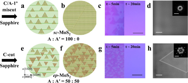 Figure 1
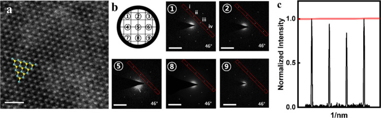 Figure 2
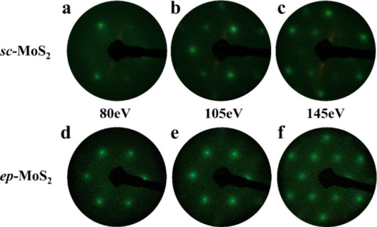 Figure 3
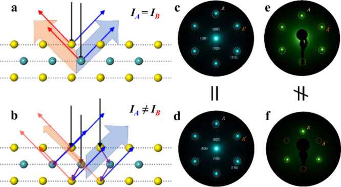 Figure 4
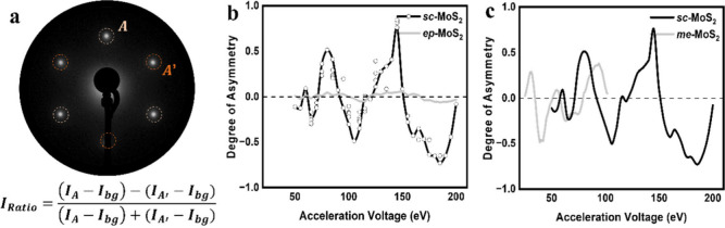 Figure 5
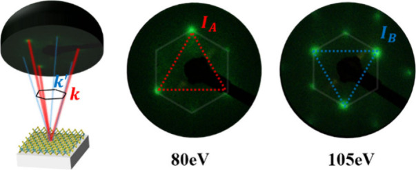 Figure 6
 Figure 7
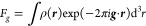 Figure 8
- —Gwangju Institute of Science and Technology10.13039/501100002582
- —National Research Foundation of Korea10.13039/501100003725
- —National Research Foundation of Korea10.13039/501100003725
- —National Research Foundation of Korea10.13039/501100003725
- —Ministry of Science and ICT, South Korea10.13039/501100014188
Peer Reviews
No public reviews on file for this paper yet. If you reviewed it on a platform where reviews are public (OpenReview, ICLR, NeurIPS, ICML), you can paste yours below so the community can read it here.
Videos
No videos yet. Explain this paper in a talk, walkthrough, or lecture? Add one.
Taxonomy
Topics2D Materials and Applications · Graphene research and applications · Surface and Thin Film Phenomena
Two-dimensional transition metal dichalcogenides (TMDs) have emerged as promising materials for next-generation electronic, optoelectronic, and photonic devices, owing to their tunable band gaps, strong light–matter interactions, and feasibility of wafer-scale integration. ?−? ? ? ? ? ? ? ? To fully exploit these properties, it is essential to achieve and verify unidirectional growth, where all single-crystal domains share the same in-plane orientation. Because most monolayer TMDs are non-centrosymmetric, 0° and 180° twin domains can form concurrently during growth and can produce distinct crystal orientations that are not superimposable, ?−? ? giving rise to differences in valley-selective optical transitions, anisotropic charge transport, and heterostructure interface matching. ?−? ? ? ? ? Coexistence of opposite orientations inevitably generates grain boundaries, which degrade both structural quality and device performance. ?−? ? ? ? ? ? Significant progress in chemical vapor deposition (CVD) methods has enabled the large-area synthesis of high-quality monolayer TMDs, including wafer-scale unidirectional single-crystal domains. ?,?,?−? ? ? ? ? ? These developments reduce grain misalignment and defect densities and open the pathways for systematic investigation for anisotropic properties of TMDs. However, verifying the perfect unidirectionality remains challenging. When triangular single-crystal flakes are spatially isolated, one can often determine their orientation, whether “up” or “down”, by direct imaging. ?,?,? Once the domains coalesce into a continuous monolayer, this becomes far more difficult, as conventional characterization techniques typically cannot differentiate between inverted orientations in a non-destructive manner. ?,?−? ? As a result, films containing mixed orientations are sometimes misinterpreted as single crystals.
While a variety of standard analytical tools are available for probing basic structural features, many fail to resolve inverted orientations in fully merged films. Low energy electron diffraction (LEED) offers a powerful, non-destructive approach for examining surface symmetry and long-range order in 2D crystals. ?−? ? ? ? In TMD systems, the appearance of a 3-fold LEED pattern has often been presented as evidence of unidirectional growth. ?,?,?−? ? This pattern reflects a breaking of Friedel’s law, ?−? ? which states that the diffraction intensity for a reflection (h, k, l) is equal to that for (−h, −k, −l), leading to asymmetries in intensities between (h, k) and (−h, −k) spots. While such symmetry breaking has been extensively exploited in transmission electron microscopy (TEM) techniques, including convergent-beam electron diffraction (CBED) and dark-field TEM, and has also been observed in prior LEED studies of asymmetric structures, its systematic application for quantifying orientation distributions in coalesced 2D TMD monolayers has remained largely unexplored. ?−? ? ? However, the presence of a 3-fold LEED pattern alone does not prove perfect unidirectionality. It can also arise when domains of opposite orientations are present in unequal proportions, producing an apparent but not absolute orientation bias. Without careful quantification of LEED spot intensities and their variation with incident electron beam energy, it is difficult to unambiguously determine the true orientation distribution. Herein, we address this issue using monolayer molybdenum disulfide (MoS_2_) as a representative TMD system. MoS_2_ is ideal for orientation studies because of its direct band gap (∼1.8–1.9 eV) ?−? ? ? and the availability of scalable CVD methods that yield large-area, high-quality single crystals. ?,?−? ? Through systematic LEED measurements, we analyze the physical origin of diffraction intensity asymmetries, investigate their dependence on electron energy, and quantitatively determine orientation distributions. Our findings not only clarify the structural origin of the 3-fold symmetry in MoS_2_ but also establish a generalizable diffraction-based framework for verifying unidirectional growth in other TMDs, including WS_2_, MoSe_2_, and WSe_2_, as well as in van der Waals heterostructures. Furthermore, this quantitative framework for a single-crystalline monolayer serves as a fundamental study for distinguishing layer thickness and complex stacking sequences (e.g., ABA vs ABC), which requires rigorous energy-dependent analysis beyond single static imaging to resolve subtle symmetry variations. This approach provides a rigorous pathway to confirm wafer-scale single crystallinity and to guide the controlled synthesis of high-performance 2D semiconductors for device applications.
Recent significant advancements in TMD growth by the CVD method, ?,?,?−? ? ? including our previous works,? have enabled unidirectional growth of various TMDs, such as MoS_2_ and WS_2_. This unidirectional growth is generally attributed to unequal adsorption energies of orientation at 0° [120n° (n = 0, 1, and 2) denoted as A] and orientation at 180° [60 + 120n° (n = 0, 1, and 2) denoted as B] on single-crystal stepped vicinal substrates, which favor alignment in one predominant orientation. We have recently summarized and compared various characterization techniques for analyzing unidirectional growth of TMDs in our review,? providing a framework for selecting appropriate methods depending on the growth stage and sample form. The most convincing evidence for this phenomenon has traditionally been the direct observation of triangular domains aligned in the same direction before they merge into a continuous film. ?,?,? However, for practical applications, it is essential to demonstrate unidirectionality even after these domains coalesce into a full film, necessitating a reliable method for verifying the orientation in a fully merged sample. Polarized Raman spectroscopy,? photoluminescence (PL), ?,? and second harmonic generation (SHG) measurements are well-known to exhibit orientation-dependent signals in TMD materials. ?,?,?−? ? However, because both incident and detected light remain unaffected by an inverted symmetry, it is generally not possible to distinguish A from B; i.e., these techniques can easily differentiate an orientation angle such as 0° from 30°, while the orientations of 0° (A) and 60°, 180°, or 300° (B) appear effectively identical. These spectroscopic methods can confirm the coexistence of the A and B domains only indirectly by identifying the grain boundaries between them. While X-ray diffraction cannot distinguish inverted orientations of non-centrosymmetric crystals, electron diffraction can distinguish between them owing to the different types of diffraction sources, radiation (X-ray) and charged particle (electron). ?,?,? To study LEED of single-crystal MoS_2_ (sc-MoS_2_) and epitaxially grown MoS_2_ with nearly equal populations of A and B orientations (ep-MoS_2_), two different types of monolayer 2H MoS_2_ films were synthesized using an inorganic molecular CVD (imCVD) method reported in our previous studies (Figure). ?,?,? For the imCVD process, C/A-1° miscut sapphire substrates and usual C-cut sapphire substrates were used for sc-MoS_2_ and ep-MoS_2_, respectively. To elucidate the crystallographic characteristics of the synthesized sc-MoS_2_ and ep-MoS_2_ samples, standard single-crystal characterization techniques were employed. ?,? The initial examination involved categorizing grown MoS_2_ into partially grown (Figurea and e) and fully grown (Figureb and f) stages. For 5 min of growth on a C/A-1° miscut sapphire substrate, sc-MoS_2_ exhibited the formation of triangular, unidirectionally aligned 2H MoS_2_ monolayers, consistent with previously reported observations (Figurec). ?,?,?,? In contrast, partially grown ep-MoS_2_ on a C-cut sapphire substrate displayed an equivalent distribution of A and B orientation grains (Figureg). However, in the fully grown stage, the distinction between sc-MoS_2_ and ep-MoS_2_ became indiscernible via optical microscopy. An additional scanning electron microscopy (SEM) image of sc-MoS_2_ is shown in Figure S3. Scanning transmission electron microscopy (STEM) and selected area electron diffraction (SAED) analyses revealed the concurrent presence of A and B orientation domains within the ep-MoS_2_ samples (Figureh). In contrast, Figures and ?d show consistent SAED patterns of sc-MoS_2_, indicating a uniform atomic orientation in the regions analyzed (Figured).
In particular, Figurea presents an atomic resolution high-angle annular dark-field STEM (HAADF–STEM) image of the 2H MoS_2_ monolayer acquired from area 5 of the TEM grid, clearly revealing a unidirectionally aligned MoS_2_ monolayer structure. SAED patterns were collected from nine distinct positions across the sample, as indicated by the grid overlay in Figureb. The corresponding SAED intensity line profiles for each position (Figurec and Figure S4c) consistently exhibit an intensity enhancement at the ii spots (B orientation) relative to that at the iii spots (A orientation) at all measured locations. Statistical validation of each normalized SAED intensity was conducted by t tests for the sc-MoS_2_ film (see the Supporting Information). This result provides strong evidence that synthesized MoS_2_ exclusively adopts the A orientation rather than a mixture of the A and B orientations. This uniformity, along with the additional SAED patterns from the remaining nine locations (Figure S4b), confirms the single-crystalline characteristics of the entire film with a globally aligned orientation. Furthermore, the atomic resolution HAADF–STEM images (Figure S5) also confirm that sc-MoS_2_ was grown in a unidirectional manner. Figure shows the LEED patterns measured on large-area sc-MoS_2_ samples depending on the E-beam energy. While a 6-fold LEED pattern is observed at certain E-beam energy, obvious 3-fold LEED patterns are observed on sc-MoS_2_ (Figurea–c). However, 3-fold LEED patterns appear in an inverted configuration depending on the E-beam energy. On the contrary, ep-MoS_2_ exhibits a 6-fold LEED pattern, independent of the energy of the electron beam (Figured–f). Although the influence of electron beam energy on this phenomenon will be discussed in detail later, these data already confirm that LEED patterns exhibiting 3-fold symmetry can effectively distinguish between A and B orientations. Technically, the structure factor (F _ g ) for a monolayer MoS_2, written for an incident electron wave, can differ from its inversion counterpart not only in amplitude but also in phase. Consider that the scattering amplitude in the kinematic sense is
where the term ρ(** r ) effectively represents the electrostatic potential distribution of the 2D layer. When this distribution lacks inversion symmetry, i.e., ρ( r ) ≠ ρ(− r **), equality F _ g _ = F _–g _ can no longer be assumed. While the resulting differences between F _ g _ and F _–g _ might be subtle when probing the sample with high-energy X-rays (Figurea), especially under conditions minimizing multiple scattering, LEED presents a different scenario (Figureb). Under LEED conditions, electrons with kinetic energies in the tens of electron volts range exhibit strong dynamical interactions. Electrons, being charged particles, interact strongly with the Coulomb potential of the atomic nuclei and core electrons within the crystal. This interaction is mediated by the exchange of virtual photons, a fundamental process in quantum electrodynamics (QED). The lower kinetic energy of the electrons in LEED enhances the interaction cross section, leading to multiple scattering events. In contrast, X-rays, being electromagnetic waves, primarily interact with the electron density through Thomson scattering. The interaction cross section for Thomson scattering is significantly smaller than that for Coulomb scattering, resulting in weaker interactions and a dominance of single-scattering events. Therefore, X-rays, being uncharged, do not interact with the periodic potential in the same manner as charged particles,
Therefore, uncharged X-rays do not interact with the periodic potential in the same manner as charged particles, which renders them relatively insensitive to subtle differences in surface registry, stacking, or domain orientation. Consequently, the diffraction patterns of sc-MoS_2_ and eq-MoS_2_ are largely indistinguishable under X-ray measurements (Figurec and d). By contrast, in LEED, where low-energy electrons interact relatively strongly with the surface periodic potential and undergo significant dynamical scattering, fine differences in symmetry and stacking give rise to distinct diffraction signatures, leading to repeated scattering channels, where each “step” in the reciprocal space modifies the amplitude according to the product of the structure factors and the phase factors. If the structure lacks inversion symmetry, these multistep scattering processes do not cancel out in a way that would equalize the intensities of ** g ** vs −** g **. Consequently, the difference in intensities can become significantly amplified in LEED, sometimes to the point of being visually apparent in the diffraction pattern as a noticeable imbalance among nominally symmetry-related spots (Figuree and f). An additional point is that, in a monolayer, the potential the electrons experience is strongly two-dimensional. The reflection geometry of LEED further means that the electron wave may partially reflect from the underlying substrate interface or vacuum boundary, introducing interference that can sharpen or enhance any existing asymmetry. Therefore, in a monolayer of sc-MoS_2_, distinct, non-equivalent intensities can be seen for, say, (1, 0) and (1, 0) in the LEED pattern at specific energies (Figure S7).
It is important to contrast LEED with electron diffraction in TEM, because the markedly different electron energies and scattering geometries give rise to distinct multiple-scattering characteristics and differential sensitivities to inversion symmetry. During TEM measurements, a high-energy electron beam of about 60–300 keV passes through the sample. Even with an extremely thin specimen, such as monolayer MoS_2_, strong interactions with the crystal lattice can induce multiple scattering, making diffraction intensities dependent on both the magnitudes and phases of the structure factors. However, the ultrathin thickness of monolayer MoS_2_ at around 0.65 nm can limit the extent to which these dynamical effects fully evolve in TEM.
Although recent studies have reported 3-fold LEED patterns as evidence of unidirectional growth, systematic investigations into this phenomenon have been insufficient. ?,?−? ?,?−? ?,?,? For instance, numerous studies lack details on the precise E-beam energy value or do not clarify which diffraction spot along the ** k ** or ** k′ ** direction exhibits the stronger intensity. Practically, this LEED-based discrimination is valuable to verifying the structural quality and orientation of the sample. If a monolayer MoS_2_ region shows a ring-shaped distribution of diffraction, it usually originates from a polycrystalline structure. Alternatively, a 6-fold symmetry with no obvious intensity mismatch is more consistent with two overlapping mirror-symmetric sublattices. In contrast, a 3-fold or asymmetrical arrangement of intensities has been suggested as evidence that the domain is unidirectionally oriented. However, we again emphasize that this merely reflects an imbalance between the populations of A and B domains rather than indicating a perfectly unidirectional orientation. To provide detailed information to demonstrate the unidirectionality of MoS_2_ with LEED analysis, we extracted LEED I–V curves for each of these main points by systematically measuring LEED images over a range of electron beam energies (for example, 50–200 eV) (Figurea). All LEED patterns used to extract I–V curves are shown in Figures S7 and S8. This method offers insight into how the electronic wave interacts with the topmost atomic plane under varying conditions of dynamical scattering. Indeed, the amplitude and phase of the structure factors responsible for each of these spots will shift as the electron wavelength changes, leading to distinct maxima and minima in the intensity profiles.
In Figureb, sc-MoS_2_ exhibited extrema in the intensity ratio at 60, 65, 80, 105, 145, and 185 eV. In contrast, the intensity ratio of eq-MoS_2_ converged to zero across the entire energy range. The significant intensity difference between A(** g ) and A′(− g ) spots in sc-MoS_2_ but not in the eq-MoS_2_ sample is a direct manifestation of the inelastic scattering resulting from broken inversion symmetry and the three-layered structure of the 2H MoS_2_ monolayer, amplified by the dynamical scattering conditions inherent in LEED. The origin of this asymmetry can be understood through a dynamic scattering model of electron diffraction. The key factor differentiating sc-MoS_2_ from eq-MoS_2_ lies in the presence (or absence) of long-range crystalline order and inversion symmetry. In sc-MoS_2_, the 2H polytype structure, consisting of three atomic layers stacked in a specific S–Mo–S sequence, lacks inversion symmetry. This asymmetry manifests in F _ g _, which, for an incident electron wave, can differ from its F _–g _ not only in amplitude but also in phase, where ρ( r ) = ρ(− r ) is effectively the electrostatic potential distribution of the 2D sheet and when ρ( r **) one can no longer assert F _ g _ = F _–g _ (eq). As previously mentioned, the distinct interaction mechanisms of electrons and X-rays with the crystal lattice lead to enhanced multiple scattering in LEED. Under LEED conditions, electrons exhibit strong dynamical interactions, and this leads to repeated scattering channels.
For comparison, Figurec plots our data alongside I–V curves obtained from μ-LEED measurements on mechanically exfoliated MoS_2_ (me-MoS_2_) on a SiO_2_ substrate, which are the previously reported μ-LEED data? for comparison. While both data sets exhibit similar overall trends, a noticeable shift in the patterns is observed. This shift can be attributed to strain effects arising from substrate interactions in epitaxially grown MoS_2_ on sapphire, which are absent in me-MoS_2_ on SiO_2_. ?,? Moreover, in the case of μ-LEED, the grain orientation is not uniquely defined and the distinction between A and B orientations was made without accounting for substrate effects. Consequently, our results provide more reliable and standard reference data for analyzing sc-MoS_2_ films epitaxially grown on sapphire substrates.
These findings can be rationalized within the framework of the dynamic scattering theory. In sc-MoS_2_, the absence of inversion symmetry amplifies multistep scattering effects, producing clear intensity asymmetries between nominally equivalent diffraction spots and giving rise to resonance-like variations at specific electron energies. By contrast, eq-MoS_2_ lacks long-range crystalline order, and the random orientation of its constituent flakes averages out such asymmetries. As a result, the intensity ratio converges toward zero, reflecting both structural disorder and enhanced inelastic scattering. Thus, the pronounced energy-dependent asymmetry in sc-MoS_2_ and its absence in eq-MoS_2_ provide a direct structural fingerprint that distinguishes truly single-crystalline films from their polycrystalline or exfoliated counterparts.
In summary, the non-centrosymmetric characteristic of monolayer MoS_2_ explains why one can see little to no Friedel law violation in conventional X-ray diffraction yet observe distinct intensity differences in electron diffraction techniques. We explore the LEED patterns of unidirectionally grown single-crystal monolayer MoS_2_, focusing on the characteristic 3-fold diffraction features that become evident at various incident electron energies. By acquiring a series of LEED images from 50 to 200 eV and extracting the intensities of key diffraction spots, we construct I–V curves that clearly reveal the dynamic scattering resonances associated with the topmost layer of MoS_2_. We demonstrate that the three main spots, spaced by 120°, show distinct or asymmetric intensity variations, confirming both the absence of inversion symmetry in the monolayer and the unidirectional alignment of the triangular domains. These findings suggest that LEED I–V analysis can serve as a robust diagnostic tool to determine monolayer orientation, confirm single-crystal behavior, and potentially refine structural parameters for monolayer TMDs. The observations presented here fill a gap in the literature, where prior discussions of 3-fold LEED in MoS_2_ were mostly qualitative and did not systematically link the energy-dependent evolutions of intensity to the underlying lattice asymmetry and growth directionality. The synergy of non-centrosymmetric structure factors and multiple scattering thus provides a clear demonstration of inversion symmetry breaking at the atomic scale, highlighting why LEED is such a powerful tool for analyzing monolayer TMD surfaces and confirming unidirectionally grown crystals. Overall, our results may serve as a guideline for applying LEED to the analysis of single-crystalline, non-centrosymmetric 2D materials beyond MoS_2_.
Supplementary Material
The reference list from the paper itself. Each links out to its DOI / PubMed record.
- 1Mak K. F.Lee C.Hone J.Shan J.Heinz T. F.Atomically thin Mo S 2: a new direct-gap semiconductor Phys. Rev. Lett.20101051313680510.1103/Phys Rev Lett.105.13680521230799 · doi ↗ · pubmed ↗
- 2Radisavljevic B.Radenovic A.Brivio J.Giacometti V.Kis A.Single-layer Mo S 2 transistors Nat. Nanotechnol.20116314715010.1038/nnano.2010.27921278752 · doi ↗ · pubmed ↗
- 3Ganatra R.Zhang Q.Few-layer Mo S 2: a promising layered semiconductor ACS Nano 2014854074409910.1021/nn 405938 z 24660756 · doi ↗ · pubmed ↗
- 4Splendiani A.Sun L.Zhang Y.Li T.Kim J.Chim C.-Y.Galli G.Wang F.Emerging photoluminescence in monolayer Mo S 2 Nano Lett.20101041271127510.1021/nl 903868 w 20229981 · doi ↗ · pubmed ↗
- 5Kumar N.Najmaei S.Cui Q.Ceballos F.Ajayan P. M.Lou J.Zhao H.Second harmonic microscopy of monolayer Mo S 2 Phys. Rev. B 2013871616140310.1103/Phys Rev B.87.161403 · doi ↗
- 6Zhang K.Zhang T.Cheng G.Li T.Wang S.Wei W.Zhou X.Yu W.Sun Y.Wang P.Interlayer transition and infrared photodetection in atomically thin type-II Mo Te 2/Mo S 2 van der Waals heterostructures ACS Nano 20161033852385810.1021/acsnano.6b 0098026950255 · doi ↗ · pubmed ↗
- 7Nassiri Nazif K.Daus A.Hong J.Lee N.Vaziri S.Kumar A.Nitta F.Chen M. E.Kananian S.Islam R.High-specific-power flexible transition metal dichalcogenide solar cells Nat. Commun.2021121703410.1038/s 41467-021-27195-734887383 PMC 8660876 · doi ↗ · pubmed ↗
- 8Li C.Cao Q.Wang F.Xiao Y.Li Y.Delaunay J.-J.Zhu H.Engineering graphene and TM Ds based van der Waals heterostructures for photovoltaic and photoelectrochemical solar energy conversion Chem. Soc. Rev.201847134981503710.1039/C 8CS 00067 K 29736528 · doi ↗ · pubmed ↗