Oxide Semiconductor for Advanced Memory Architectures: Atomic Layer Deposition, Key Requirement and Challenges
Chi-Hoon Lee, Seong-Hwan Ryu, Taewon Hwang, Sang-Hyun Kim, Yoon-Seo Kim, Jin-Seong Park

TL;DR
This review explores how oxide semiconductors, deposited via atomic layer deposition, can be used in next-generation low-power memory devices and highlights the challenges in their integration.
Contribution
The paper provides a comprehensive review of oxide semiconductors and ALD techniques for next-generation memory applications, emphasizing material design and integration challenges.
Findings
Oxide semiconductors offer low leakage current and compatibility with 3D architectures, making them suitable for advanced memory devices.
Atomic layer deposition enables precise growth of high-quality oxide semiconductor films with controllable properties.
Key challenges include contact resistance, hydrogen instability, and the lack of p-type materials in oxide semiconductor memory applications.
Abstract
This review outlines the emergence of oxide semiconductors as promising channel materials for high-density, low-power next-generation memory applications.Adsorption and reaction mechanisms of atomic layer deposition have enabled the design of high-performance oxide semiconductors for next-generation memory applications.This review discusses key challenges toward successfully integrating oxide semiconductors into next-generation memory devices. This review outlines the emergence of oxide semiconductors as promising channel materials for high-density, low-power next-generation memory applications. Adsorption and reaction mechanisms of atomic layer deposition have enabled the design of high-performance oxide semiconductors for next-generation memory applications. This review discusses key challenges toward successfully integrating oxide semiconductors into next-generation memory…
Genes, proteins, chemicals, diseases, species, mutations and cell lines named across the full text — each resolved to its canonical identifier and authoritative record.
Click any figure to enlarge with its caption.
 Figure 1
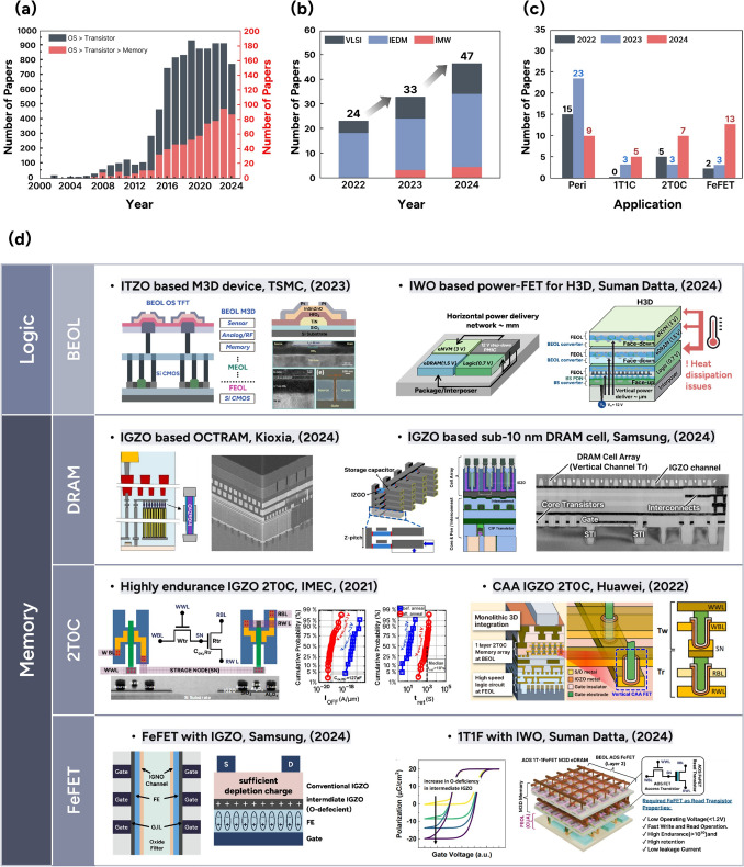 Figure 2
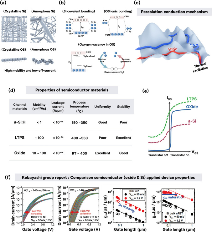 Figure 3
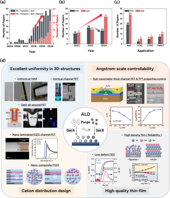 Figure 4
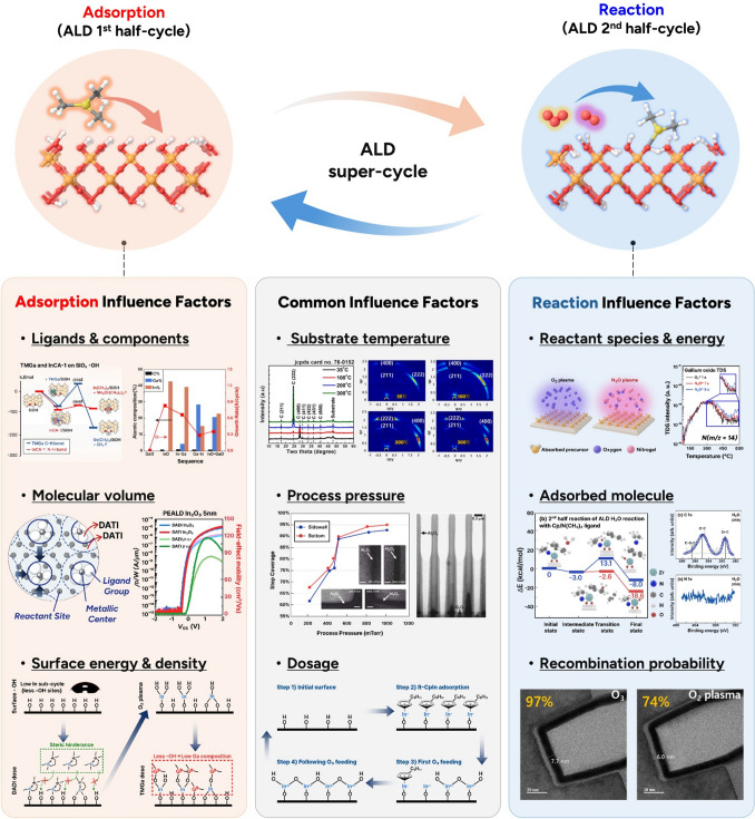 Figure 5
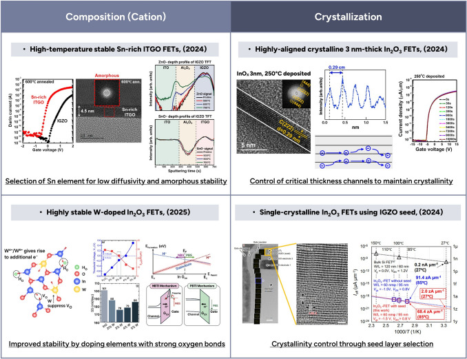 Figure 6
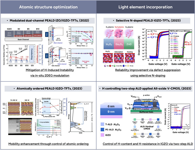 Figure 7
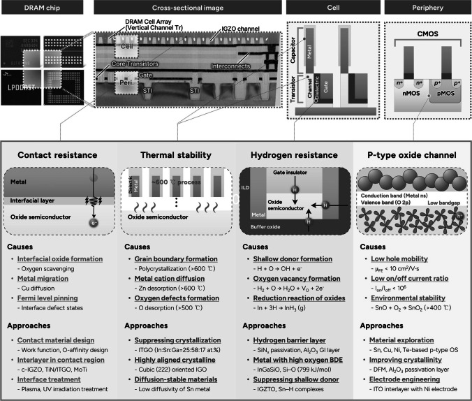 Figure 8
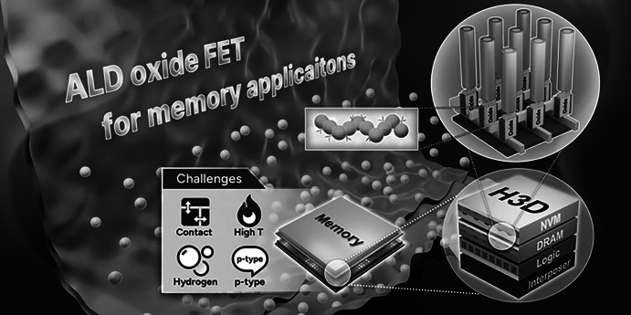 Figure 9
Peer Reviews
No public reviews on file for this paper yet. If you reviewed it on a platform where reviews are public (OpenReview, ICLR, NeurIPS, ICML), you can paste yours below so the community can read it here.
Videos
No videos yet. Explain this paper in a talk, walkthrough, or lecture? Add one.
Taxonomy
TopicsSemiconductor materials and devices · Electronic and Structural Properties of Oxides · Ferroelectric and Negative Capacitance Devices