Overcoming Material Incompatibility via 2D Free‐Surface Engineering
Youcef A. Bioud, Meriem Bouchilaoun, Waldemar Schreiber, Redouane Amrar, Gilles Patriarche, Tao Ma, Jens Ohlmann, Ali Soltani, David Lackner, Stefan Janz

TL;DR
A new method reduces defects in mismatched materials by creating a 2D free surface, improving the quality of heteroepitaxial structures for electronics.
Contribution
A scalable post-epitaxial approach introduces a 2D free surface to decouple mismatched layers and reduce defects.
Findings
The 2DFS interface significantly reduces strain-related defects in Ge/Si heterostructures.
Advanced microscopy and optical analyses confirm bulk-like material quality in scalable heterostructures.
Defect annihilation is attributed to the surrounding free surfaces, validated by electron microscopy and photoluminescence.
Abstract
Heteroepitaxy has been pivotal in advancing both optoelectronics and microelectronics, driving the development of faster, more efficient devices across diverse applications. However, achieving high material quality remains challenging due to lattice mismatches. Strain induced by variations in lattice parameters and thermal properties provides additional degrees of freedom for material tailoring but often leads to dislocation generation, wafer bowing, and cracking. These issues are addressed through a scalable post‐epitaxial approach that strategically targets the misfit dislocation network, leading to the creation of a sub‐nanometric 2D free surface (2DFS). This interface effectively decouples the epilayer from the substrate, significantly reducing strain‐related defects. Scalable heterostructures exhibited pronounced defect annihilation, as demonstrated by electron microscopy, defect…
Genes, proteins, chemicals, diseases, species, mutations and cell lines named across the full text — each resolved to its canonical identifier and authoritative record.
Click any figure to enlarge with its caption.
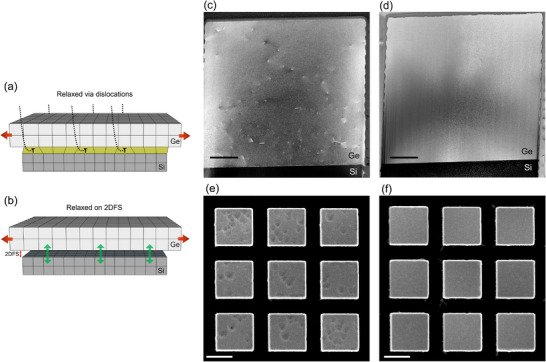 Figure 1
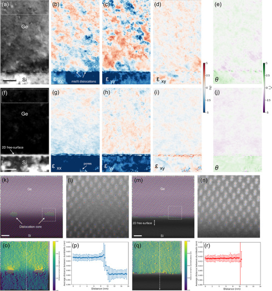 Figure 2
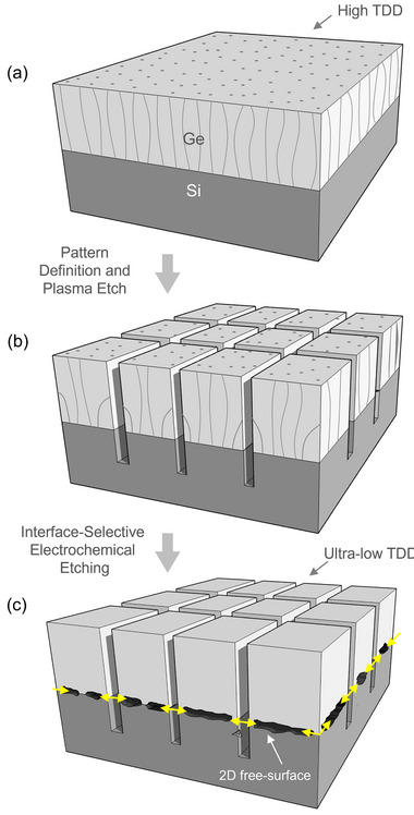 Figure 3
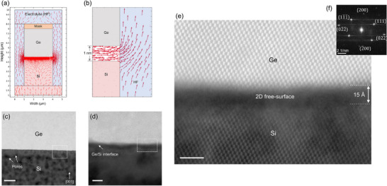 Figure 4
 Figure 5
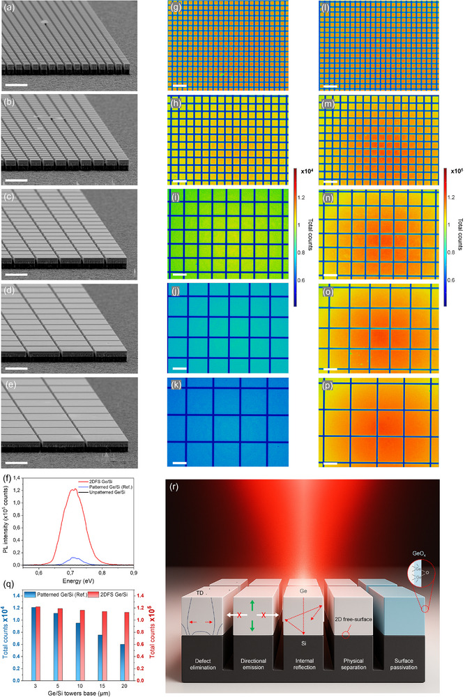 Figure 6
 Figure 7
Peer Reviews
No public reviews on file for this paper yet. If you reviewed it on a platform where reviews are public (OpenReview, ICLR, NeurIPS, ICML), you can paste yours below so the community can read it here.
Videos
No videos yet. Explain this paper in a talk, walkthrough, or lecture? Add one.
Taxonomy
TopicsNanowire Synthesis and Applications · Semiconductor materials and devices · GaN-based semiconductor devices and materials