Defect-engineered competition between exciton annihilation and trapping in MOCVD WS2
Ruofei Zheng, Leon Daniel, Dedi Sutarma, Christian Viernes, Yingfang Ding, Tobiloba Fabunmi, Gerd Bacher, Michael Heuken, Holger Kalisch, Andrei Vescan, Peter Kratzer, Marika Schleberger, Germán Sciaini

TL;DR
The paper shows how defects in WS2 monolayers affect exciton decay processes, offering a way to control optoelectronic properties through defect engineering.
Contribution
The study provides a quantitative framework for defect-modulated exciton decay in MOCVD WS2 using combined spectroscopy and modeling.
Findings
Defect trapping and exciton annihilation compete based on defect-to-exciton density ratio (~3.5).
Defect saturation at high exciton densities suppresses defect trapping.
Rate constants for defect trapping and annihilation are 0.02 cm² s⁻¹ and 0.1 cm² s⁻¹, respectively.
Abstract
Exciton dynamics critically influence the optoelectronic performance of two-dimensional transition metal dichalcogenides (TMDCs). In large-scale WS2 monolayers grown via metal–organic chemical vapor deposition (MOCVD), intrinsic sulfur vacancies introduce in-gap states that promote nonradiative recombination through defect trapping (DT). Under elevated excitation conditions, the decay behaviour changes as exciton–exciton annihilation (EEA) emerges as a competing nonradiative process. To investigate these mechanisms across excitation regimes, we combine steady-state quantum efficiency measurements with femtosecond broadband transient absorption spectroscopy on samples with varying defect concentrations. These complementary measurements provide an unprecedented quantitative disentanglement of these decay pathways, a level of analysis not previously reported for MOCVD-grown monolayer WS2.…
Genes, proteins, chemicals, diseases, species, mutations and cell lines named across the full text — each resolved to its canonical identifier and authoritative record.
Click any figure to enlarge with its caption.
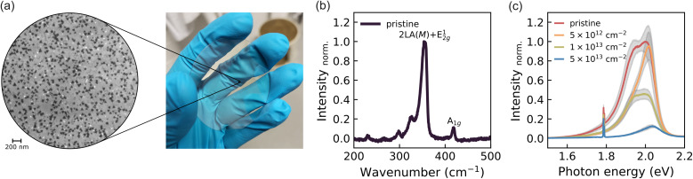 Figure 1
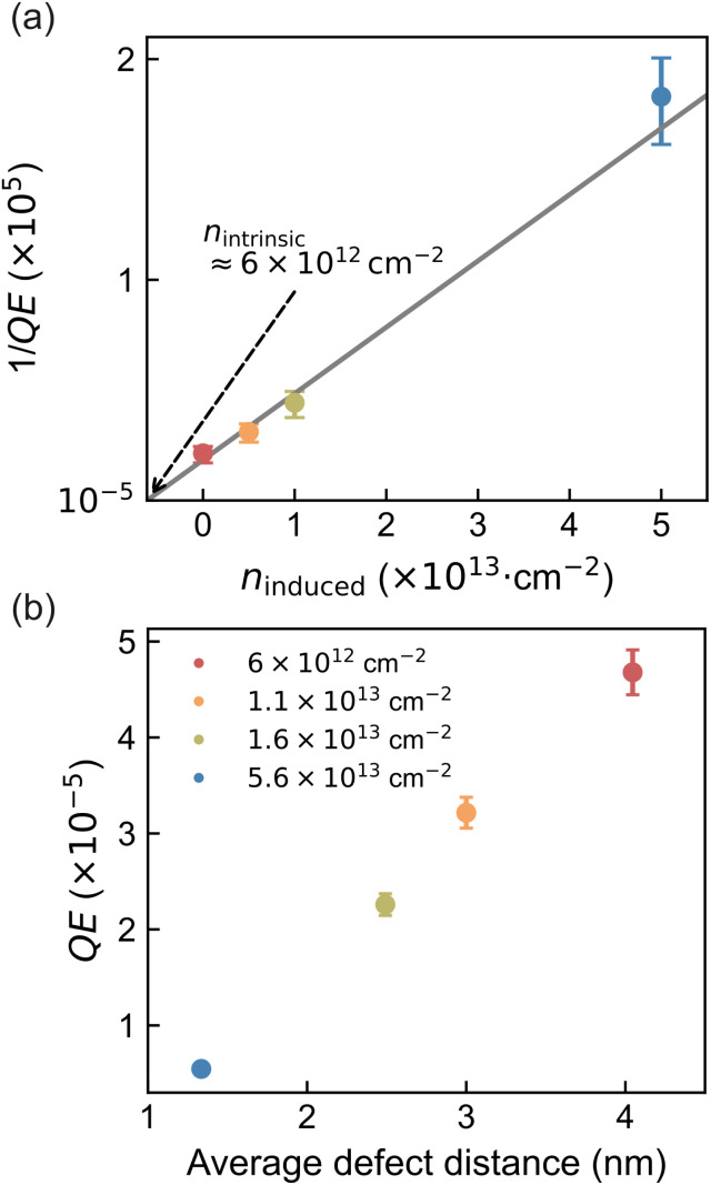 Figure 2
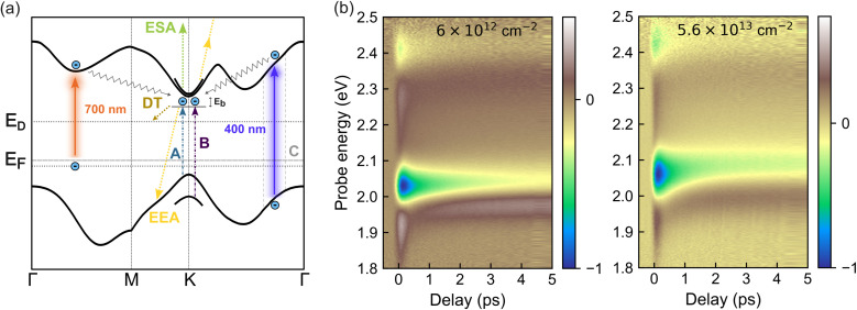 Figure 3
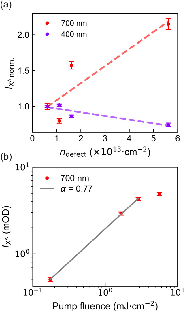 Figure 4
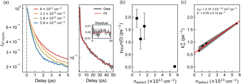 Figure 5
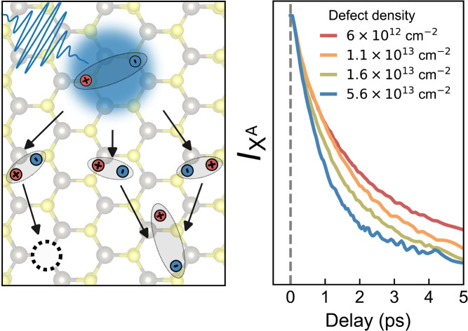 Figure 6
 Figure 7
 Figure 8
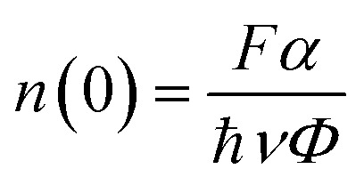 Figure 9
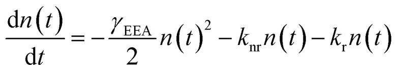 Figure 10
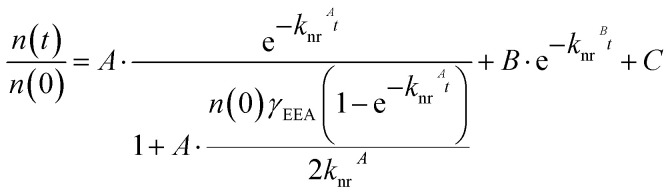 Figure 11
 Figure 12
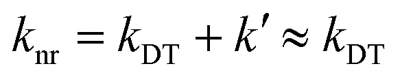 Figure 13
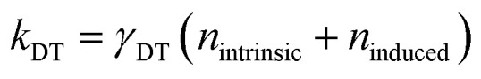 Figure 14
Peer Reviews
No public reviews on file for this paper yet. If you reviewed it on a platform where reviews are public (OpenReview, ICLR, NeurIPS, ICML), you can paste yours below so the community can read it here.
Videos
No videos yet. Explain this paper in a talk, walkthrough, or lecture? Add one.
Taxonomy
Topics2D Materials and Applications · Perovskite Materials and Applications · Organic Electronics and Photovoltaics