Advanced BCl3-Driven Deep Ion Etching of β-Ga2O3 for Precision High-Aspect-Ratio Nanostructures
Badriyah Alhalaili

TL;DR
This paper presents a new deep etching method for gallium oxide that enables the creation of precise nanostructures for use in harsh environments.
Contribution
The study introduces an advanced BCl3-driven deep ion etching technique for β-Ga2O3 with improved etching depth and precision.
Findings
A deep ion-etching process for Ga2O3 achieved etches of 6.97 µm.
The method enables high-aspect-ratio nanostructures suitable for robust nanosensors.
The technique improves chemical stability and etching uniformity for Ga2O3.
Abstract
Gallium oxide-based devices are critical in various applications, including industrial safety, the gas and petroleum sectors, and research environments. However, the deep etching process has not been thoroughly explored. Key parameters such as etching rate, selectivity, uniformity, isotropic/anisotropic behavior, and surface properties all influence the effectiveness of the etching process and its reproducibility. This research was motivated by the need for efficient fabrication processes, particularly in applications where sensors must operate in harsh environments, due to their instead of owning to low leakage current density of their power devices. In this study, we studied a deep etching technique for Ga2O3, focusing on the chemical stability of the two planes and identifying suitable protocols that could enhance etching depth via a dry-etching process. A deep ion-etching process…
Genes, proteins, chemicals, diseases, species, mutations and cell lines named across the full text — each resolved to its canonical identifier and authoritative record.
Click any figure to enlarge with its caption.
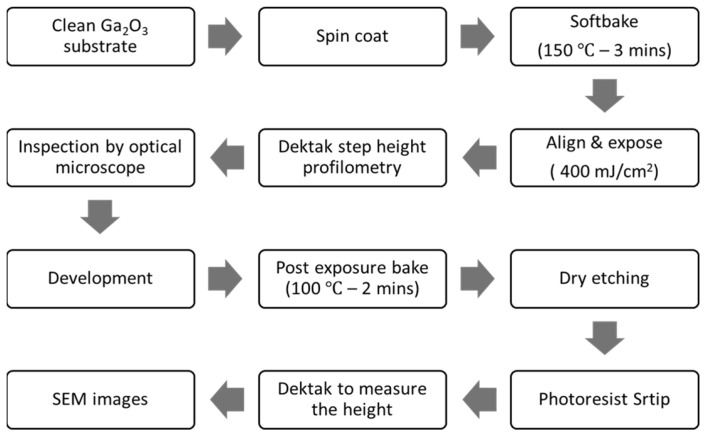 Figure 1
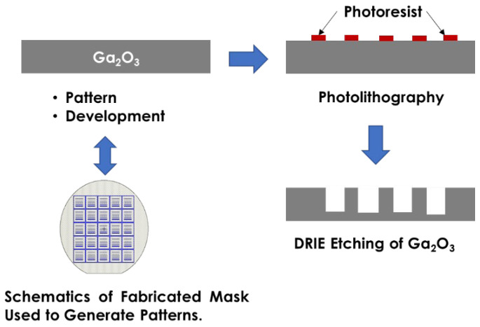 Figure 2
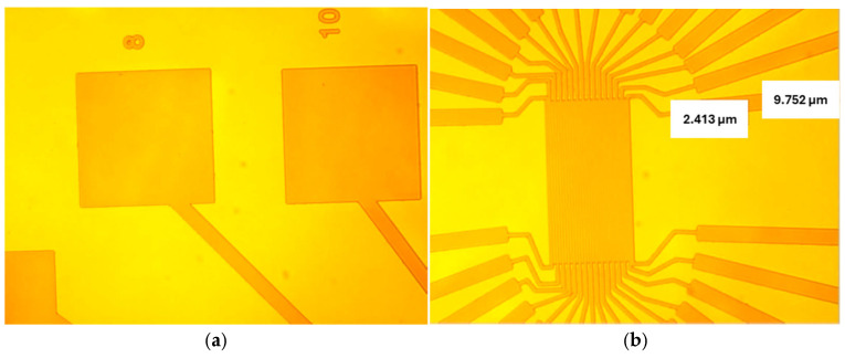 Figure 3
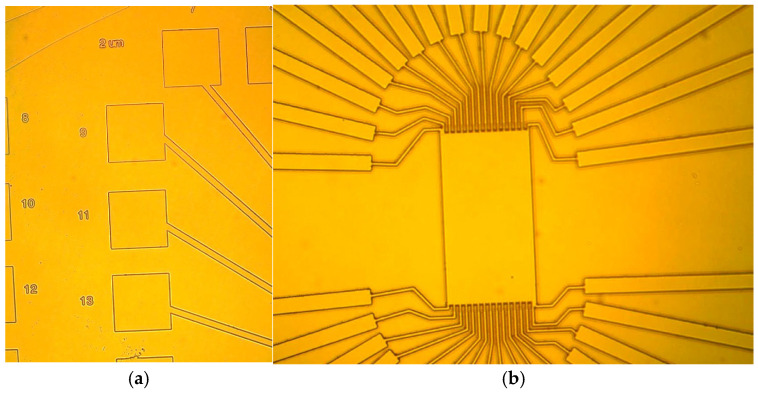 Figure 4
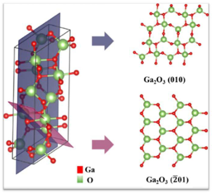 Figure 5
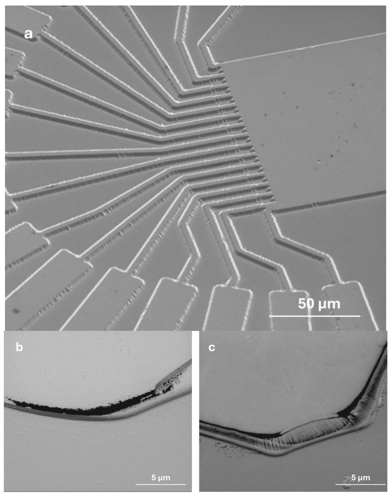 Figure 6
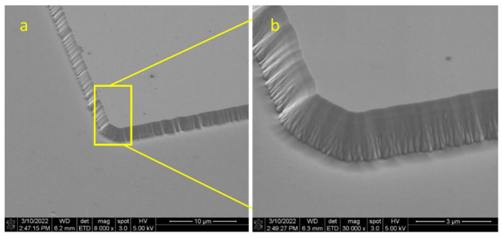 Figure 7
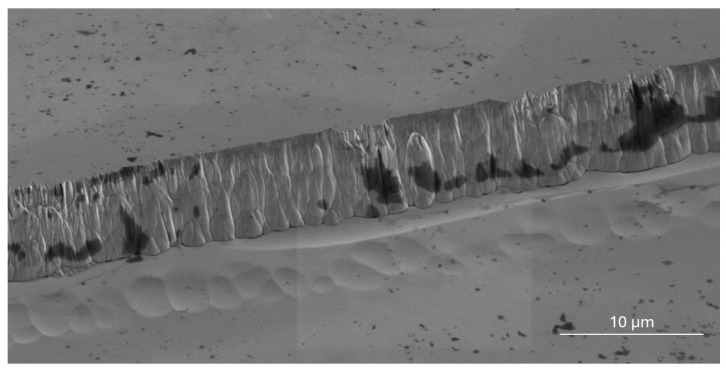 Figure 8
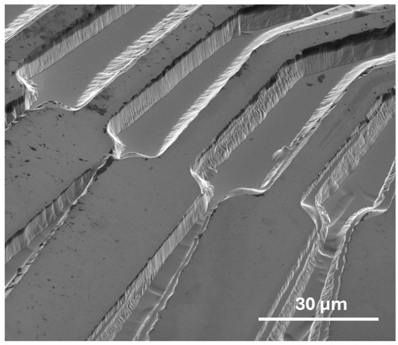 Figure 9
Peer Reviews
No public reviews on file for this paper yet. If you reviewed it on a platform where reviews are public (OpenReview, ICLR, NeurIPS, ICML), you can paste yours below so the community can read it here.
Videos
No videos yet. Explain this paper in a talk, walkthrough, or lecture? Add one.
Taxonomy
TopicsGa2O3 and related materials · GaN-based semiconductor devices and materials · Copper-based nanomaterials and applications