Electron diffraction and dark-field TEM for structural analysis of 2D van der Waals materials
Byunghyun Kim, Daesung Park, Siwon Jeong, Hyobin Yoo

TL;DR
This paper reviews how electron microscopy techniques help study structural variations in 2D van der Waals materials and their impact on physical properties.
Contribution
The paper highlights recent advances in combining electron diffraction and dark-field imaging to study structural degrees of freedom in 2D materials.
Findings
Electron diffraction and dark-field TEM reveal structural variations like stacking domains and corrugations.
These techniques enable real-time observation of structural changes under external stimuli.
They connect structural evolution directly to functional behavior in 2D van der Waals materials.
Abstract
Two-dimensional (2D) van der Waals materials possess structural degrees of freedom that set them apart from conventional bulk crystals and strongly influence their physical properties. Such freedom, enabled by the weak interlayer bonding, permits stacking, twisting, and lateral sliding of layers, leading to structural variations such as out-of-plane corrugations, layer-number–dependent electronic and optical responses, and interlayer registry variations that produce stacking domains with distinct functionalities. Capturing and understanding these variations is essential for linking structure to function. Transmission electron microscopy (TEM) offers complementary approaches for this purpose: electron diffraction provides quantitative crystallographic fingerprints, while dark-field (DF) imaging translates selected diffraction information into spatial maps of local structure. When…
Genes, proteins, chemicals, diseases, species, mutations and cell lines named across the full text — each resolved to its canonical identifier and authoritative record.
Click any figure to enlarge with its caption.
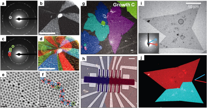 Figure 1
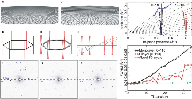 Figure 2
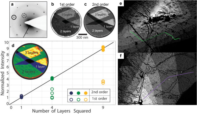 Figure 3
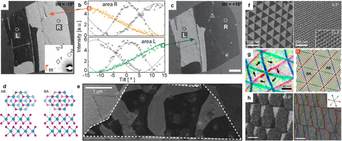 Figure 4
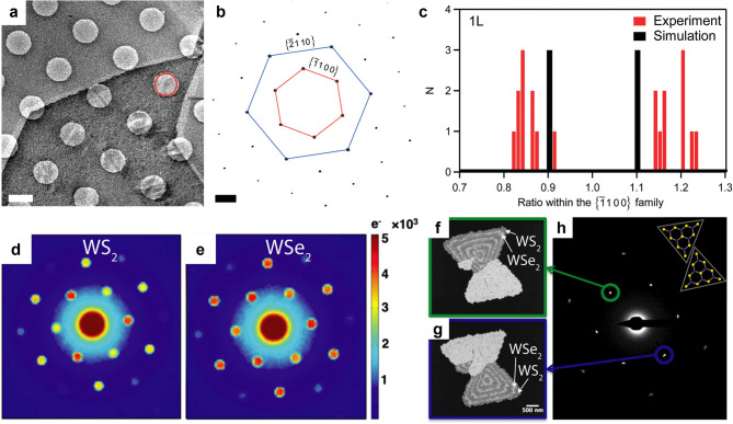 Figure 5
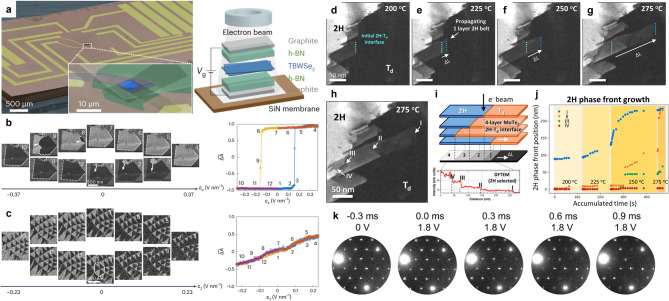 Figure 6
- —http://dx.doi.org/10.13039/501100003725National Research Foundation of Korea
Peer Reviews
No public reviews on file for this paper yet. If you reviewed it on a platform where reviews are public (OpenReview, ICLR, NeurIPS, ICML), you can paste yours below so the community can read it here.
Videos
No videos yet. Explain this paper in a talk, walkthrough, or lecture? Add one.
Taxonomy
Topics2D Materials and Applications · Graphene research and applications · Transition Metal Oxide Nanomaterials
Introduction
Two-dimensional (2D) van der Waals materials have transformed the landscape of materials science by offering atomic-scale control over structure and properties. The weak interlayer bonding characteristic of these materials allows individual atomic planes to be isolated and manipulated in ways that are not possible in conventional bulk crystals (Novoselov et al. 2004; Zhang et al. 2005). This structural flexibility facilitates stacking (Dean et al. 2010; Britnell et al. 2012a, b; Haigh et al. 2012; Geim and Grigorieva 2013; Gong et al. 2014; Hong et al. 2014; Tongay et al. 2014; Cui et al. 2015), twisting (Li et al. 2010; Yankowitz et al. 2012; Dean et al. 2013; Liu et al. 2014a; Woods et al. 2014; Kim et al. 2016), and lateral sliding of layers (Li and Wu 2017; Yasuda et al. 2021; Vizner Stern et al. 2021; Wang et al. 2022a; Weston et al. 2022; Meng et al. 2022; Ko et al. 2023; Sui et al. 2023), enabling access to a rich configurational phase space. These degrees of freedom not only create opportunities for material design but also fundamentally alter electronic (Bistritzer and MacDonald 2011; Luican et al. 2011; Hunt et al. 2013; Ponomarenko et al. 2013; Liu et al. 2020; Regan et al. 2020; Wang et al. 2020), optical (Britnell et al. 2013; Fang et al. 2014; Ceballos et al. 2015; Rivera et al. 2015, 2016; Sunku et al. 2018; Jin et al. 2019), mechanical (Lee et al. 2008; Hod 2012; Liu et al. 2014b; Jiang and Park 2014), and ferroic properties (Li and Wu 2017; Yasuda et al. 2021; Vizner Stern et al. 2021; Wang et al. 2022a; Weston et al. 2022; Meng et al. 2022; Sui et al. 2023; Zhong et al. 2017; Gong et al. 2019; Sharpe et al. 2019; Zheng et al. 2020; Wu et al. 2022). With the discovery of correlated and topological phases in twisted bilayer graphene (Cao et al. 2018a, b; Yankowitz et al. 2019; Saito et al. 2020; Park et al. 2021) and ferroelectricity in twisted hexagonal boron nitride (h-BN) (Yasuda et al. 2021; Vizner Stern et al. 2021) and transition metal dichalcogenides (TMDs) (Wang et al. 2022a; Weston et al. 2022; Meng et al. 2022; Ko et al. 2023), structural degrees of freedom have become as critical as chemical composition in determining functionality.
Understanding and exploiting this structural tunability requires precise, spatially resolved structural analysis tools. Transmission electron microscopy (TEM) offers two complementary modes: electron diffraction and dark-field (DF) imaging. Electron diffraction provides quantitative crystallographic information, revealing lattice symmetries (Song et al. 2010; Geng et al. 2012; Gao et al. 2015a; Zhou et al. 2015; Ahn et al. 2018), three-dimensional distortions (Meyer et al. 2007a, b; Kirilenko et al. 2011; Thomsen et al. 2017), strain states (Ahn et al. 2017; Kim et al. 2019; Thodkar et al. 2024), and interlayer orientations with high angular precision (Thodkar et al. 2024; Brown et al. 2012; Yuk et al. 2014; Dumcenco et al. 2015; Latychevskaia et al. 2019; Sung et al. 2019, 2022a; Yoo et al. 2019). DF imaging uses selected diffraction spots to transform this reciprocal-space information into real-space contrast, enabling the direct visualization of orientation domains (Huang et al. 2011; Kim et al. 2011; Rasool et al. 2011; Tsen et al. 2012; Lee et al. 2013), stacking boundaries (Ko et al. 2023; Yoo et al. 2019; Alden et al. 2013; Lin et al. 2013; Butz et al. 2014; Park et al. 2025), and stacking sequences (Brown et al. 2012; Yoo et al. 2019; Alden et al. 2013; Lin et al. 2013; Butz et al. 2014; Ping and Fuhrer 2012). By combining these approaches, one can directly connect diffraction-based structural fingerprints with spatial maps of local variations, capturing subtle structural modulations that are otherwise difficult to detect. This integration makes TEM uniquely capable of resolving the complex structural landscape of 2D materials across multiple length scales and under diverse experimental conditions.
Moreover, the combined use of electron diffraction and DF imaging is highly adaptable to in-situ and operando experiments. Diffraction patterns acquired during thermal cycling, electrical biasing, or mechanical deformation can track changes in lattice constants, strain distributions, phases, and stacking configurations in real time (Gao et al. 2015b; Fei et al. 2016; Zheng et al. 2022). At the same time, DF imaging can map the spatial evolution of these transformations, revealing how domains nucleate, migrate, or reorganize under external stimuli (Ko et al. 2023; Alden et al. 2013; Lee et al. 2023; Winkle et al. 2024; Zhang et al. 2024). This dual capability is particularly valuable as it offers a direct link between structural changes and functional responses with both spatial and temporal resolution.
In this review, we discuss the application of the combined electron diffraction and DF TEM imaging to the structural analysis of 2D van der Waals materials. We emphasize how these techniques reveal crystallinity, three-dimensional structural modulation, stacking order variations from bilayer to multilayer systems, and structural symmetry-related phenomena. We also examine their use in in-situ and operando studies, where structural dynamics under external stimuli can be captured in real time. By covering both the fundamental principles and recent advances, this review aims to provide a comprehensive framework for utilizing electron diffraction and DF imaging as complementary tools for understanding and engineering the structural degrees of freedom in 2D materials.
Large-area orientation and grain boundary analysis
Grain boundaries and rotational grains play a critical role in determining the macroscopic behavior of 2D materials, especially those grown by scalable techniques including chemical vapor deposition (CVD) method. In such samples, rotational disorder, small-angle and high-angle grain boundaries introduce variations in carrier mobility (Tsen et al. 2012; Yazyev and Louie 2010; Yu et al. 2011; Song et al. 2012; Clark et al. 2013; van der Zande et al. 2013; Ly et al. 2016), strain accumulation (Azizi et al. 2014; Elibol et al. 2017; Han et al. 2018a, b; Xie et al. 2018), and interfacial reactivity (Kim et al. 2014; Yasaei et al. 2014; Rong et al. 2015; Fan et al. 2018; Zhu et al. 2019). Capturing these features over statistically relevant areas while maintaining crystallographic sensitivity requires a technique that bridges the gap between atomic-resolution imaging and bulk-scale structural probes.
DF TEM meets this need by enabling large-area orientation mapping through Bragg spot–filtered imaging. In a typical workflow, a selected area electron diffraction (SAED) pattern is acquired from the region of interest (Fig. 1a), and an objective aperture is used to isolate a specific diffraction vector. The resulting DF image (Fig. 1b) displays the spatial distribution of lattice planes corresponding to that diffraction condition. By repeating this process across multiple non-equivalent Bragg peaks, a complete orientation map can be constructed. Color-coding the DF images obtained from different spots enables visualization of grain orientation, misorientation angles, and boundary distributions with sub-micrometer spatial resolution (Fig. 1c, d) (Huang et al. 2011; Kim et al. 2011; Tsen et al. 2012; Lee et al. 2013).
Fig. 1. Grain orientation and grain boundary analysis. (a-b) In graphene with differently oriented grains, the SAED pattern (a) and the DF image (b) (Scale bar, 500 nm) obtained from the circled spot in (a) are shown. (c-d) Multiple diffraction spots selected in SAED (c) were used to construct the corresponding color-coded image of graphene (d) (Scale bar, 500 nm). (e-f) ADF-STEM image of two grains and their boundary (e), with the pentagon–heptagon pairs highlighted in (f). Scale bar, 5 Å. Adapted with permission (Huang et al., 2011). Copyright Springer Nature. (g-h) Color-coded DF image (g) of polycrystalline graphene consisting of grains ~ 50 μm in size, and the device fabricated on a single grain boundary (h). Scale bars, 1 μm. Adapted with permission (Tsen et al., 2012). Copyright the American Association for the Advancement of Science. (i-j) Bright-field (BF) image (i) of a monolayer MoS₂ consisting of two grains, along with its SAED pattern (inset), and the color-coded DF image (j) reconstructed from selected diffraction spots in SAED. Adapted with permission (van der Zande et al., 2013). Copyright Springer Nature
This approach has been particularly powerful in monolayer and few-layer graphene, where CVD growth often results in a patchwork of rotational grains (Rasool et al. 2011; Lee et al. 2013). DF TEM has revealed large-angle grain boundaries separating grains misoriented by 20° to 30°, as well as low-angle boundaries formed by wrinkle-induced strain during transfer. Mapping these features over tens of microns enables direct correlation with electrical measurements such as local conductivity and carrier scattering. In one example, DF TEM (Fig. 1c, d) was combined with atomic-resolution annular dark-field scanning TEM (ADF-STEM) (Fig. 1e, f) to identify 27° grain boundaries composed of periodic pentagon–heptagon dislocation cores in monolayer graphene (Huang et al. 2011). In related work, Tsen et al. (2012) used DF TEM (Fig. 1g) to locate and resolve grain boundaries in polycrystalline graphene before fabricating Hall bar devices intersecting these boundaries with sub-50 nm alignment accuracy (Fig. 1h). Electrical transport across boundaries with known structures showed that well-connected, atomically sharp boundaries had only slightly reduced conductance compared to single grains, whereas poorly stitched boundaries containing amorphous or overlapping regions could be up to an order of magnitude more resistive.
Beyond graphene, DF TEM orientation mapping has been applied to other 2D semiconductors such as CVD-grown monolayer MoS_2 _(van der Zande et al. 2013). In that work, large triangular single-crystal grains exceeding 100 μm were confirmed to be continuous, while polycrystalline films were resolved into distinct grains separated by tilt or mirror twin boundaries. DF TEM (Fig. 1i, j), combined with atomic-resolution STEM, showed that tilt boundaries were stitched by lines of non-hexagonal rings and that mirror twin boundaries produced distinct contrast due to the sublattice asymmetry of Mo and S atoms. Correlation with optical and transport measurements revealed that mirror twins caused photoluminescence quenching but little change in in-plane conductivity, while certain tilt boundaries enhanced photoluminescence but slightly reduced electrical conductance. These results highlight how DF TEM, when combined with complementary high-resolution imaging, can directly connect grain boundary structures to the optical and electronic responses of 2D semiconductors.
In addition to DF TEM orientation mapping, the accompanying SAED provides further insight into the crystallographic structure. While the angular distribution of diffraction spots in SAED reveals the in-plane orientation of individual grains, the intensity ordering of these spots provides information about the out-of-plane lattice orientation or equivalently the 2D chirality. In low-symmetry monolayers such as triclinic ReS_2_, this chirality originates from the loss of inversion symmetry when a monolayer is supported on a substrate, resulting in two enantiomeric configurations that differ in whether the layer faces upward or downward with respect to the substrate. Therefore, the diffraction spots of the \documentclass[12pt]{minimal} \usepackage{amsmath} \usepackage{wasysym} \usepackage{amsfonts} \usepackage{amssymb} \usepackage{amsbsy} \usepackage{mathrsfs} \usepackage{upgreek} \setlength{\oddsidemargin}{-69pt} \begin{document}$$\:\left\{100\right\}$$\end{document} planes also exhibit chirality, with their intensity sequence appearing in either a clockwise or a counterclockwise order. Their handedness can thus be directly identified from SAED patterns (Chen et al. 2024; Jiang et al. 2025). These studies demonstrate that electron diffraction provides diverse crystallographic information across a wide range of 2D materials.
Quantification of three-dimensional structural modulation
Unlike conventional bulk crystals, 2D materials can exhibit significant out-of-plane distortions caused by thermal fluctuations, intrinsic rippling, or strain relaxation (Meyer et al. 2007b; Fasolino and Los 2007; Ishigami et al. 2007; Obraztsov et al. 2007; Xu et al. 2014; Bronsgeest et al. 2015) (Fig. 2a, b). These corrugations are not merely morphological features but are closely linked to the fundamental stability and functionality of the material. For example, surface undulations can influence electron-phonon coupling (Mariani and Oppen 2008; Castro et al. 2010; Laitinen et al. 2014; Ng et al. 2022), modulate the band structure (Mohiuddin et al. 2009; Pereira and Castro Neto 2009; Conley et al. 2013; He et al. 2016), and thereby affect device performance. Quantifying such out-of-plane deformations with high precision is therefore a central challenge in the field.
Fig. 2. Diffraction analysis of corrugated graphene. (a–b) Schematic illustrations of flat graphene (a) and corrugated graphene (b). (c–d) Reciprocal rods corresponding to flat graphene (c) and corrugated graphene (d). (e) Intersection between the Ewald sphere (dashed line) and reciprocal rods under specimen tilt. (f-g) Evolution of diffraction spots with graphene tilt angles of 0° (f), 14° (g), and 26° (h). (i) Intensity profiles of diffraction peaks as a function of graphene tilt. (j) Broadening of diffraction peaks with increasing tilt angle. Adapted with permission (Meyer et al. 2007b). Copyright Springer Nature
Electron diffraction provides a sensitive and non-destructive means to probe corrugations through analysis of the shape and broadening of Bragg reflections (Meyer et al. 2007a, b; Kirilenko et al. 2011; Thomsen et al. 2017). In TEM, the diffraction pattern corresponds to the intersection of the reciprocal lattice with the nearly flat Ewald sphere. For a perfectly flat 2D crystal, the reciprocal lattice consists of elongated rods perpendicular to the plane, which intersect the Ewald sphere as sharp Bragg spots regardless of specimen tilt (Fig. 2c). In contrast, a corrugated membrane has a distribution of local surface normals, which modifies the reciprocal lattice from straight rods to cone-like shapes (Fig. 2d). As the specimen is tilted, the intersection of the Ewald sphere with these cones produces Bragg spots that broaden (Fig. 2e and f-h). By quantifying this tilt-dependent broadening (Fig. 2i), one can extract the statistical distribution of local tilt angles (Fig. 2j).
Tilt-series diffraction experiments on suspended monolayer graphene have shown cone-like broadening with cone angles of approximately 8° to 11°, corresponding to surface-normal variations of about 5° to 6°. In bilayer graphene, the variation in surface normal was found to be 2° presumably due to the increase in the membrane stiffness (Meyer et al. 2007a, b).
While analogous tilt-series diffraction broadening analyses are well established for graphene, extending the same protocol to other 2D materials such as h-BN (Pan et al., 2012), TMDs (Brivio et al. 2011; Shao et al. 2022), and In_2_Se_3 _(Zheng et al., 2022) remains an opportunity. Given their differing elastic constants and common processing routes, including substrate-supported growth and polymer-assisted transfer, one would expect material-specific corrugation signatures and wrinkle-induced distortions. Systematic, diffraction-based comparisons across layer numbers, substrates, and processing conditions would help quantify how process history shapes the final morphology.
Layer number identification in 2D materials
The number of atomic layers in 2D materials critically influences their electronic (Zhang et al. 2009; Li et al. 2014a; Xi et al. 2016; Zhou et al. 2016), optical (Ferrari et al. 2006; Nair et al. 2008; Li et al. 2013; Zhang et al. 2014), and ferroic properties (Meng et al. 2022; Gong et al. 2017; Huang et al. 2017; Deng et al. 2018). For example, TMDs including MoS_2_, MoSe_2_, WS_2_, and WSe_2_ exhibit a thickness dependent transition from a direct to an indirect bandgap (Mak et al. 2010; Splendiani et al. 2010; Jin et al. 2013; Zhao et al. 2013; Li et al. 2014b), while multilayer structures show interlayer-registry–driven phenomena such as emergent phases and symmetry-dependent functionalities (Yasuda et al. 2021; Vizner et al. 2021; Wang et al. 2022a; Weston et al. 2022; Tsen et al. 2015; Yoshida et al. 2015; Fei et al. 2018) . In TEM, the layer number can be determined without atomic-resolution imaging by exploiting the sensitivity of specific diffraction intensities to the number of scattering planes. This relationship is governed by the crystal’s structure factor, which reflects the arrangement of atoms within the unit cell and incorporates the interference between electron waves scattered from successive layers.
For certain layered crystals with specific symmetries, such as the hexagonal lattice of graphene, particular orders of Bragg reflections can be selected to determine the number of layers with high accuracy. In graphene, for example, the second-order Bragg peaks ( \documentclass[12pt]{minimal} \usepackage{amsmath} \usepackage{wasysym} \usepackage{amsfonts} \usepackage{amssymb} \usepackage{amsbsy} \usepackage{mathrsfs} \usepackage{upgreek} \setlength{\oddsidemargin}{-69pt} \begin{document}$$\:g=11\bar{2}0$$\end{document} ) exhibit an intensity that scales approximately with the square of the number of layers (∝N^2^) under kinematic conditions. This strong thickness dependence enables robust layer-number identification in DF TEM images. Selecting this reflection with the objective aperture in DF TEM mode produces contrast in which brighter regions correspond to thicker layers, allowing monolayer, bilayer, and few-layer regions to be discriminated over large fields of view with high spatial resolution (Fig. 3a–c).
Fig. 3. Layer number identification of graphene by DF TEM. (a-c) SAED of few-layer graphene (a), along with the first-order DF image from the dashed circle (b) and the second-order DF image from the solid circle (c). (d) Intensity variation in the first- and second-order DF images as a function of the number of layers; inset shows color-coded DF images of the same region as in (b) and (c). Adapted with permission (Shevitski et al., 2013). Copyright American Physical Society. (e-f) Second-order DF images of few-layer graphene, up to 7 layers. Adapted with permission from (Ping et al., 2012). Copyright American Chemical Society
The structure-factor dependence of diffraction intensity, including its sensitivity to both layer number and stacking symmetry, has been quantitatively calculated and validated experimentally (Shevitski et al. 2013). These calculations demonstrated how specific diffraction conditions can enhance or suppress certain reflections depending on symmetry, and the experiments confirmed that these effects hold in real samples (Fig. 3d). Other reports also provided direct experimental evidence of layer-number–dependent contrast by showing that DF TEM images formed from the second-order Bragg reflection ( \documentclass[12pt]{minimal} \usepackage{amsmath} \usepackage{wasysym} \usepackage{amsfonts} \usepackage{amssymb} \usepackage{amsbsy} \usepackage{mathrsfs} \usepackage{upgreek} \setlength{\oddsidemargin}{-69pt} \begin{document}$$\:g=11\stackrel{-}{2}0$$\end{document} ) (Fig. 3e, f) exhibit increased intensity with layer number up to approximately seven layers (Ping and Fuhrer 2012).
Although this approach has been most extensively developed and systematically applied to graphene, it is gradually being extended to other 2D materials. For example, three-dimensional electron diffraction patterns obtained under specimen tilt have enabled clear distinction between monolayer and multilayer in h-BN (Pan et al. 2012; Odlyzko and Mkhoyan, 2012) and α-RuCl_3_ (Yang et al. 2023). Similarly, the layer number of anisotropic black phosphorus has been roughly estimated from the intensity ratios among diffraction spots (Castellanos-Gomez et al. 2014). Together, these studies established both the theoretical framework and the experimental validation for using structure-factor selected reflections to map layer number and, under suitable conditions, stacking symmetry in 2D materials (Sung et al. 2019).
Stacking order identification and domain boundary mapping
In bilayer graphene, the most commonly studied stacking orders are Bernal (AB) and its mirror-symmetric counterpart (BA). Although these differ only by an in-plane translation and are electronically similar in flat samples, they can exhibit contrasting DF TEM intensities due to phase interference between electron waves diffracted from the two layers (Brown et al. 2012; Sung et al. 2019; Yoo et al. 2019; Alden et al. 2013; Lin et al. 2013; Butz et al. 2014). When a first-order Bragg reflection (e.g., \documentclass[12pt]{minimal} \usepackage{amsmath} \usepackage{wasysym} \usepackage{amsfonts} \usepackage{amssymb} \usepackage{amsbsy} \usepackage{mathrsfs} \usepackage{upgreek} \setlength{\oddsidemargin}{-69pt} \begin{document}$$\:g=10\bar{1}0$$\end{document} ) is used for imaging under exact zone-axis conditions, the path-length difference between scattered waves in AB and BA domains has the same magnitude but opposite sign, producing identical diffraction intensities and thus no DF contrast. Tilting the sample away from the zone axis modifies the phase term in the bilayer’s structure-factor such that one stacking moves toward more constructive interference while the other moves toward more destructive interference. At certain tilt angles, this difference is maximized, yielding strong stacking-dependent diffraction contrast (Fig. 4a-c). This principle, first demonstrated in DF TEM studies of bilayer graphene (Brown et al. 2012; Yoo et al. 2019; Alden et al. 2013; Lin et al. 2013; Butz et al. 2014), established that AB and BA domains can be unambiguously mapped over large areas with nanometer-scale resolution.
Fig. 4DF TEM analysis of stacking configurations and domain walls. (a) First-order DF image of bilayer graphene at − 15° tilt. (inset) SAED pattern of bilayer graphene. (b) Intensity variation with specimen tilt for two areas, R (upper panel) and L (lower panel). Each curve corresponds to the intensity of spots 1, 2, and 3 in the SAED pattern inset of (a), marked by diamond, circle, and triangle, respectively. (c) First-order DF image of bilayer graphene at + 15° tilt. Scale bar, 1 μm. Adapted with permission from (Brown et al., 2012). Copyright American Chemical Society. (d) Top and side views of AB (left) and BA (right) stacking orders in bilayer MoSe_2_. (e) First-order DF image of bilayer MoSe₂ with specimen tilt. Adapted with permission (Sung et al., 2020). Copyright Springer Nature. (f) First-order DF images of twisted bilayer graphene with twist angles of 0.1° (left) and 0.4° (right). Adapted with permission (Yoo et al., 2019). Copyright Springer Nature. (g) (Left) Domain wall map of twisted bilayer graphene constructed from second-order DF images, with red, blue, and green arrows indicating the directions of the Burgers vectors of domain walls. (Right) Corresponding atomic model. Adapted from Reference (Alden et al., 2013). (h) (Left) First-order DF image of twisted trilayer graphene and (right) domain wall map constructed from second-order DF images. Scale bar, 100 nm. Adapted with permission (Park et al., 2025). Copyright Springer Nature
The same tilt-assisted DF TEM approach has been applied to other layered crystals with lower symmetries, including h-BN and TMDs such as MoS_2_ and WSe_2 _(Ko et al. 2023; Winkle et al. 2024; Kim et al. 2013; Rosenberger et al. 2020; Sung et al. 2020; Yang et al. 2024). In these systems, mirror-related domains, analogous to AB and BA in graphene and often labeled MX and XM (Fig. 4d), are observed. Here, M denotes the transition-metal atom (e.g., Mo or W), and X represents the chalcogen atom (e.g., S or Se). These domains can be distinguished using first-order Bragg reflections under optimized tilt conditions (Fig. 4e). This enables large-area mapping of stacking domains that influence valley polarization, interlayer exciton coupling, and ferroic ordering in TMDs multilayers.
In twisted 2D materials, DF TEM is a powerful tool for probing the reconstructed patterns that emerge from lattice relaxation. In these systems, periodic variations in local stacking order reorganize into low-energy domains whose distribution and connectivity critically influence the electronic and ferroic behavior. In small-angle twisted bilayer graphene, for example, relaxation produces triangular AB and BA domains separated by soliton-like boundaries that form an interconnected triangular network (Fig. 4f) (Yoo et al. 2019; Alden et al. 2013; Engelke et al. 2023). These boundaries can be directly visualized using second-order Bragg reflections such as those from the { \documentclass[12pt]{minimal} \usepackage{amsmath} \usepackage{wasysym} \usepackage{amsfonts} \usepackage{amssymb} \usepackage{amsbsy} \usepackage{mathrsfs} \usepackage{upgreek} \setlength{\oddsidemargin}{-69pt} \begin{document}$$\:11\bar{2}0$$\end{document} } family, where their visibility depends on the relationship between the reciprocal lattice vector g and the Burgers vector b (or lattice-shift vector) describing the stacking change across the boundary (Yoo et al. 2019; Lin et al. 2013; Butz et al. 2014; Engelke et al. 2023). Imaging with multiple inequivalent second-order reflections allows for the identification of which boundary sets vanish in each image, enabling assignment of the Burgers vector to each family and quantitative mapping of the dislocation network (Fig. 4g).
In twisted trilayer graphene, multiple stacking sequences such as Bernal-type (ABA, ACA) and rhombohedral-type (ABC, ACB) can coexist with very small energy differences. This near-degeneracy drives complex reconstruction in which competing stackings form multi-scale domain structures. DF TEM is particularly effective for resolving these patterns, as shown by Park et al., (2025) where selective imaging of specific Bragg reflections revealed the spatial arrangement and connectivity of competing domains along with their boundary characteristics (Fig. 4h). Using first-order Bragg reflections under optimized tilt conditions, ABC, ACB, and Bernal stackings can be distinguished, while second-order reflections can be used to identify the Burgers vectors of the boundaries, thereby determining the specific stacking change across each domain wall. Such mapping is key to understanding how stacking configuration influences the electronic structure and the emergence of correlated ground states.
Revealing lattice symmetry through Friedel pair breaking
In monolayer TMDs with trigonal prismatic coordination, such as MoS_2_ (Fig. 5a) and WS_2_, the absence of an in-plane inversion center gives rise to a well-defined crystallographic polarity. This polarity, defined by the orientation of the metal–chalcogen sublattice, underpins valley-contrasting optical selection rules (Xiao et al. 2012; Mak et al. 2013) and layer-dependent ferroelectric phenomena (Wang et al. 2022a; Weston et al. 2022). In electron diffraction, polarity can be probed by comparing the intensities of a Friedel pair of reflections, g and − g. Under the assumptions of kinematic scattering and weak phase objects, Friedel’s law predicts these intensities to be identical, producing an inversion-symmetric diffraction pattern.
Fig. 5. Polarity analysis through diffraction intensity. (a) Low-magnification TEM image of MoS₂. Scale bar, 1 μm. (b) SAED of the region marked with red circle in (a). Scale bar, 2 nm^− 1^. (c) Histogram of the intensity ratios between neighboring diffraction spots of the \documentclass[12pt]{minimal} \usepackage{amsmath} \usepackage{wasysym} \usepackage{amsfonts} \usepackage{amssymb} \usepackage{amsbsy} \usepackage{mathrsfs} \usepackage{upgreek} \setlength{\oddsidemargin}{-69pt} \begin{document}$$\:\left\{\bar{1}100\right\}$$\end{document} family in (b). Adapted with permission from (Brivio, et al., 2011). Copyright American Chemical Society. (d-e) Diffraction intensities of WS₂ (d) and WSe_2_ (e). (f-h) Polarity maps obtained by DF TEM, imaged from the diffraction spots marked with the green (f) and blue (g) circles in the SAED pattern (h), respectively, showing distinct contrasts. Adapted with permission (Deb et al., 2020). Copyright Elsevier
In practice, however, monolayer TMDs often exhibit Friedel pair breaking (Fig. 5b, c), where conjugate Bragg peaks display measurable intensity differences (van der Zande et al. 2013; Brivio et al. 2011; Deb et al. 2020; Ahn et al. 2024). Traditionally, such violations of Friedel’s law have been attributed to multiple scattering in thick, non-centrosymmetric crystals. Recent analysis and experiment have shown that even an atomically thin polar crystal can break Friedel symmetry when its in-plane inversion symmetry is absent (Deb et al. 2020). In this case, higher-order terms in the scattered wavefunction—representing multiple scattering paths that originate from the same atom—become significant, particularly for strong phase objects such as WS_2_ that contain heavy elements (Fig. 5d, e). These effects lead to polarity-dependent intensity asymmetry between g and − g, regardless of the incident beam energy.
By selecting an appropriate Bragg reflection sensitive to polarity and forming a DF TEM image from either g or − g, polar domains can be directly visualized over large areas. Regions of opposite polarity appear with inverted contrast when switching between the two conjugate reflections, enabling unambiguous domain mapping (Fig. 5f–h). This approach has been used to identify polar twins, rotational variants, and more complex polar textures in monolayer TMDs, providing a fast and non-destructive method for assessing polarity-related structural organization in 2D materials.
In-situ/operando TEM
The combination of electron diffraction and DF TEM, when implemented under in-situ and operando conditions, offers a unique way to monitor the structural processes occurring in 2D materials under external stimuli. These techniques can distinguish structural variants such as different crystal phases (Zheng et al. 2022; Lee et al. 2023; Gavhane et al. 2021; Wang et al. 2022b), charge-density-wave (CDW) modulations (Danz et al. 2021; Sung et al. 2022b, 2024; Domröse et al. 2024; Durham et al. 2024), or stacking domains (Ko et al. 2023; Alden et al. 2013; Winkle et al. 2024; Zhang et al. 2024), all of which directly influence the functional properties of the material. Because such structural states can reorganize when exposed to temperature, electric fields, or other perturbations, capturing their evolution in real time is crucial for understanding and optimizing material performance. In-situ TEM allows the structural response to be tracked during controlled perturbations, while operando TEM extends this capability to devices under realistic working conditions, enabling direct correlation between structural evolution and functional output.
In twisted h-BN and TMDs, unconventional forms of ferroelectric behavior have recently been reported, but the structural origins of these responses have remained unclear (Yasuda et al. 2021; Vizner Stern et al. 2021; Wang et al. 2022a; Weston et al. 2022). As described earlier, first-order DF TEM imaging can distinguish MX and XM stacking domains, which correspond to up- and down-polarized regions in these systems. While their static arrangement was well characterized, how these polar domains evolve under an applied electric field remained unknown, representing a key gap in linking structure to dielectric response. Ko et al. (2023) addressed this by fabricating a double-capacitor device geometry (Fig. 6a) and performing operando DF TEM imaging to follow, in real time, the reconfiguration of polar domains during electrical switching. Their measurements revealed that distinct modes of domain evolution correlate with either ferroelectric-like (Fig. 6b) or antiferroelectric-like responses (Fig. 6c), providing a clear structural origin for these behaviors and resolving prior ambiguities in the interpretation of interfacial sliding ferroelectricity. Because the temporal resolution of conventional DF TEM was insufficient to resolve the fastest domain wall motion, they used a stroboscopic measurement strategy to effectively bypass this limitation, enabling direct measurement of domain wall propagation speeds on short time scales and with the potential to extend the method into the sub-microsecond regime.
Fig. 6. Domain evolution and phase transitions in 2D materials revealed by in-situ/operando TEM. (a) Scanning electron microscope (SEM) image (left) and schematic illustration (right) of the operando TEM device. (b) In-situ snapshots (left) of polar domains in bilayer WSe_2_ under electrical bias and the corresponding ferroelectric-like response (right). (c) Snapshots (left) of alternating polar domains in twisted bilayer WSe_2_ under bias, along with the corresponding antiferroelectric-like response (right). Adapted with permission (Ko et al., 2023). Copyright Springer Nature. (d-g) DF images of MoTe_2_ after applying a 0.5 s heat pulse at (d) 200 °C, (e) 225 °C, (f) 250 °C, and (g) 275 °C, showing the T_d_–2 H phase transition. (h) DF image of MoTe_2_ at 275 °C showing a layer-by-layer T_d_–2 H phase transition. Phase fronts of mono-, bi-, tri-, and quad-layers are labeled I–IV, respectively. (i) Schematic illustration of the T_d_–2 H interfaces and corresponding intensity profile illustrating the phase fronts. (j) Temporal evolution of 2 H phase fronts during pulsed heating. Adapted with permission from (Lee et al., 2023). Copyright American Chemical Society. (k) Evolution of the diffraction pattern in 1T-TaS_2_ during heating induced by a pulse applied at 0 ms. Adapted with permission (Hart et al., 2023). Copyright Springer Nature
In another example, Lee et al. (2023) employed in-situ TEM to study the structural evolution of few-layer MoTe_2_ during its anisotropic layer-by-layer phase transition between the semiconducting 2 H phase and the semimetallic T_d_ phase (Fig. 6d-g). By combining diffraction and DF imaging, they were able to resolve the spatial progression of the transition front with high spatial and temporal resolution, revealing that the phase transformation proceeds through a sequence of discrete layer conversions rather than a uniform transformation (Fig. 6h-j). This insight clarified the microscopic pathway of a technologically important phase change relevant to phase-change memory and reconfigurable electronics.
Similarly, Hart et al. (2023) combined DF TEM with time-resolved electron diffraction to investigate how CDW order in 1T-TaS_2_ responds to applied electrical pulses (Fig. 6k). Their measurements captured the rapid suppression and reformation of the CDW superlattice, showing that defects play a decisive role in mediating the recovery pathway. This experiment demonstrated how structural modulations that govern correlated electronic states can be directly tracked under device-relevant driving, establishing a model for how to disentangle intrinsic order-parameter dynamics from extrinsic defect effects.
Beyond biasing and heating, in-situ DF TEM is increasingly integrated with other techniques. For example, in-situ cryogenic DF TEM was employed to visualize polar and phase domain walls in MoTe_2_, revealing conductive interfacial states between topologically distinct phases and demonstrating electron-beam–induced domain switching (Huang et al. 2019). In-situ straining DF TEM enabled modulation of phase and polarization in In_2_Se_3_, showing a reversible transition between ferroelectric and antiferroelectric phases under mechanical deformation (Zheng et al. 2022). DF ultrafast TEM combined with time-resolved SAED was utilized to capture photoinduced bulging and buckling dynamics in black phosphorus over nanosecond-to-microsecond timescales (Kim et al. 2020). These advances highlight the expanding role of in-situ TEM as a versatile platform for elucidating the structural dynamics of 2D materials and other quantum systems under external stimuli.
Summary and outlook
Structural degrees of freedom in 2D van der Waals materials, including twist angle, stacking order, and out-of-plane corrugations, are key determinants of their electronic, optical, and ferroic properties. This review has highlighted how the combination of electron diffraction and DF TEM offers complementary reciprocal- and real-space perspectives for resolving these structural features and linking them to functionality.
Large-area DF TEM mapping is effective for identifying grain boundaries, rotational disorder, and stacking domain distributions, while tilt-assisted imaging can be applied more generally to distinguish different stacking orders in bilayer and multilayer systems. Diffraction-based analyses, such as tilt-series broadening measurements, can quantify out-of-plane distortions with high precision. Polarity mapping, achieved by detecting intensity asymmetries between Friedel-related reflections, enables direct visualization of polar domains in non-centrosymmetric crystals, which is essential for understanding polarity-dependent optical selection rules and interfacial ferroelectricity.
Extending these approaches to in-situ and operando experiments makes it possible to monitor structural dynamics during external stimuli, including electrical switching, thermally driven phase transitions, and CDW modulations. A current limitation of DF imaging is its temporal resolution, which is constrained by signal-to-noise considerations. This can be overcome by combining DF imaging with stroboscopic acquisition methods or integrating ultrafast TEM techniques, thereby enabling the capture of rapid domain wall motion and other fast structural processes.
Looking ahead, integrating four-dimensional STEM (4D-STEM) into in-situ and operando workflows will provide multi-channel structural information—such as strain, symmetry breaking, and phase coexistence—from a single dataset, greatly enhancing the efficiency of dynamic experiments. Coupling these high-dimensional datasets with machine learning will further accelerate analysis, enabling rapid, automated, and more sensitive detection of subtle structural changes. Together, these developments will expand the scope of diffraction and DF TEM from static structural mapping to real-time, multi-parameter tracking of structure–function relationships in 2D materials under realistic operating conditions.
The reference list from the paper itself. Each links out to its DOI / PubMed record.
- 1D.S. Gavhane et al., In situ electron microscopy study of structural transformations in 2D Co Se₂. npj 2D Materials and Applications 5, 24 (2021)
- 2A.W. Tsen et al., Structure and control of charge density waves in two-dimensional 1T-Ta S₂. Proceedings of the National Academy of Sciences 112, 15054–15059 (2015)10.1073/pnas.1512092112 PMC 467906626598707 · doi ↗ · pubmed ↗