Direct Formation of Stable 1T′ Molybdenum Telluride (MoTe2) by Laser Annealing Processes as Robust Contacts for High-Performance Molybdenum Disulfide (MoS2) Field Effect Transistors
Yao-Zen Kuo, Ming-Jin Liu, Paul Albert Sino, Po-Chien Lai, Chia-Chen Chung, Yu-Chieh Hsu, Tzu-Yi Yang, Ruei-Hong Cyu, Feng-Chuan Chuang, Hao-Chung Kuo, Seokwoo Jeon, Yu-Lun Chueh

TL;DR
A new laser method creates stable, high-performance contacts for 2D transistors, enabling better performance and heat resistance.
Contribution
A scalable laser annealing process to form 1T′-MoTe2 contacts for MoS2 FETs with high thermal stability.
Findings
1T′-MoTe2 contacts enable near-zero Schottky barriers and high device performance in MoS2 FETs.
1T′-MoTe2 electrodes maintain high on/off ratios up to 500 °C, outperforming Bi contacts.
Laser-formed 1T′-MoTe2 contacts preserve MoS2 integrity and ensure large-area uniformity.
Abstract
Semimetals, with their low density of states near the Fermi level, effectively suppress metal-induced gap states, enabling near-zero Schottky barrier heights in two-dimensional (2D) field-effect transistors (FETs). However, the low melting point of semimetals (Bi, Sb) limits the applications of 2D FETs at high temperatures. Here, we introduce a robust semimetal contact strategy for high-performance MoS2 FETs, based on continuous-wave laser annealing of elemental metals (Bi, Mo, Pt, W) and tellurium to form metal tellurides. Specifically, the phase of molybdenum telluride (1T′/2H) can be prepared under different laser parameters. In particular, large-area, high-crystallinity films of stable 1T′-MoTe2 can be synthesized uniformly, and source/drain electrodes of 1T′-MoTe2 are formed directly from elemental Mo and Te without damaging the underlying MoS2. Electrical characterization shows…
Genes, proteins, chemicals, diseases, species, mutations and cell lines named across the full text — each resolved to its canonical identifier and authoritative record.
Click any figure to enlarge with its caption.
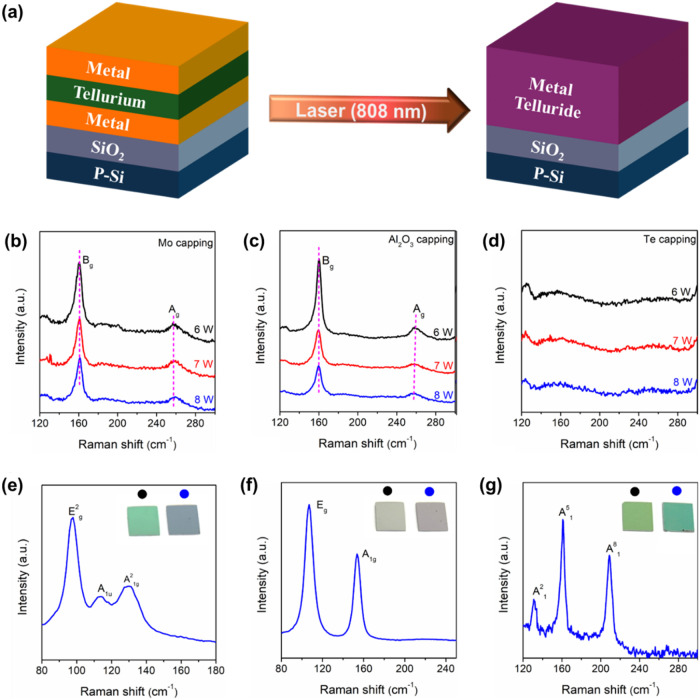 Figure 1
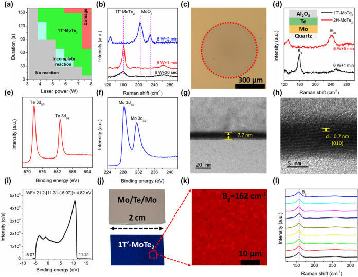 Figure 2
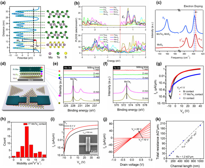 Figure 3
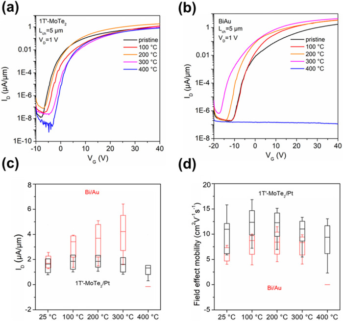 Figure 4
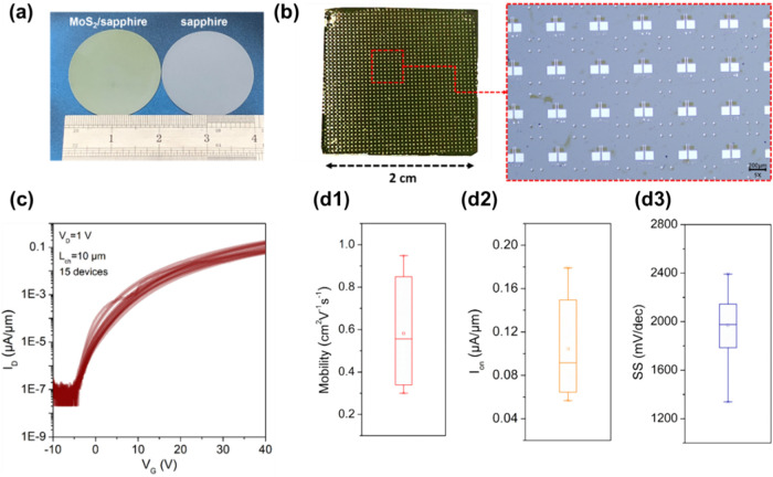 Figure 5
 Figure 6
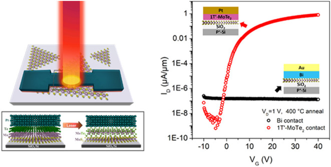 Figure 7
 Figure 8
Peer Reviews
No public reviews on file for this paper yet. If you reviewed it on a platform where reviews are public (OpenReview, ICLR, NeurIPS, ICML), you can paste yours below so the community can read it here.
Videos
No videos yet. Explain this paper in a talk, walkthrough, or lecture? Add one.
Taxonomy
Topics2D Materials and Applications · Chalcogenide Semiconductor Thin Films · Molecular Junctions and Nanostructures