A Junction Temperature Prediction Method Based on Multivariate Linear Regression Using Current Fall Characteristics of SiC MOSFETs
Haihong Qin, Yang Zhang, Yu Zeng, Yuan Kang, Ziyue Zhu, Fan Wu

TL;DR
This paper introduces a new method to predict the junction temperature of SiC MOSFETs using current fall characteristics for better thermal monitoring in power systems.
Contribution
A novel multivariate linear regression method using current fall time and loss as TSEPs for accurate junction temperature prediction in SiC MOSFETs.
Findings
Current fall time and fall loss are effective temperature-sensitive electrical parameters for SiC MOSFETs.
The proposed MLR method achieves high prediction accuracy in junction temperature estimation.
The method shows superiority over traditional single TSEP approaches in thermal sensing applications.
Abstract
The junction temperature (Tj) is a key parameter reflecting the thermal behavior of Silicon carbide (SiC) MOSFETs and is essential for condition monitoring and reliability assessment in power electronic systems. However, the limited temperature sensitivity of switching characteristics makes it difficult for traditional single temperature-sensitive electrical parameters (TSEPs) to achieve accurate estimation. To address this challenge and enable practical thermal sensing applications, this study proposes an accurate, application-oriented Tj estimation method based on multivariate linear regression (MLR) using turn-off current fall time (tfi) and fall loss (Efi) as complementary TSEPs. First, the feasibility of using current fall time and current fall energy loss as TSEPs is demonstrated. Then, a coupled junction temperature prediction model is developed based on multivariate linear…
Genes, proteins, chemicals, diseases, species, mutations and cell lines named across the full text — each resolved to its canonical identifier and authoritative record.
Click any figure to enlarge with its caption.
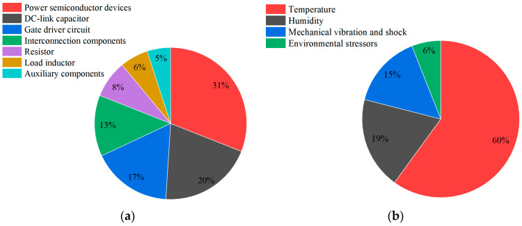 Figure 1
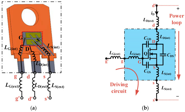 Figure 2
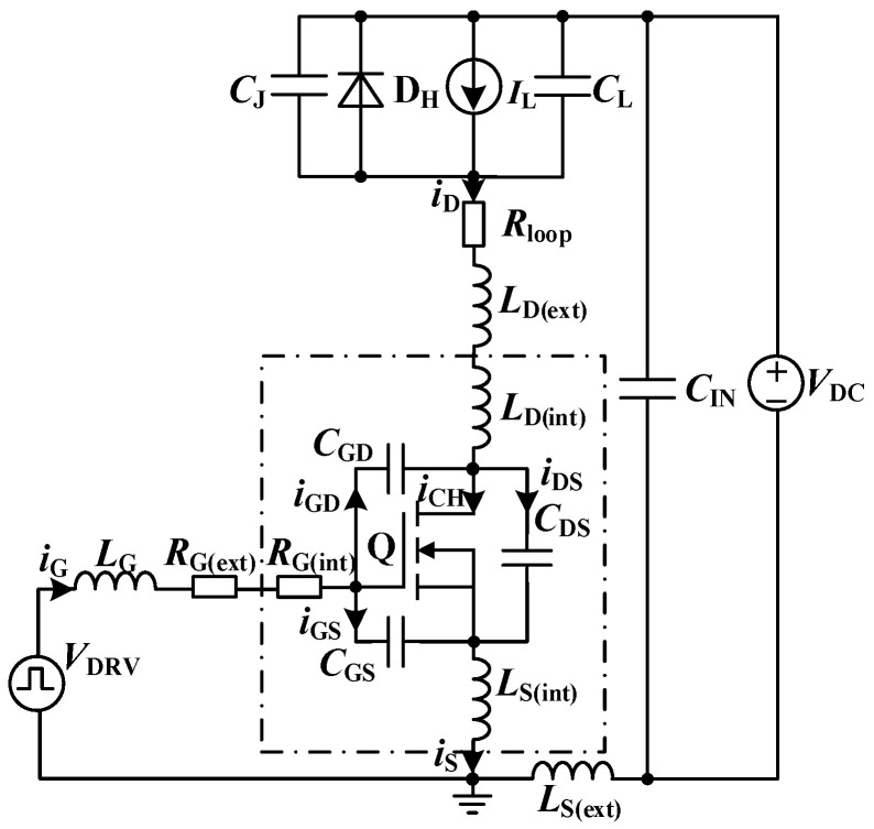 Figure 3
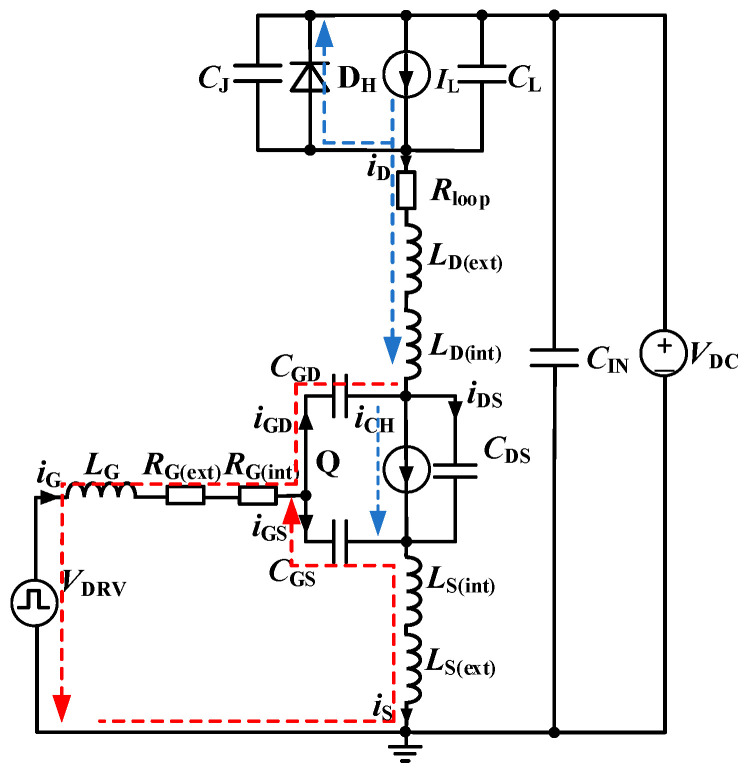 Figure 4
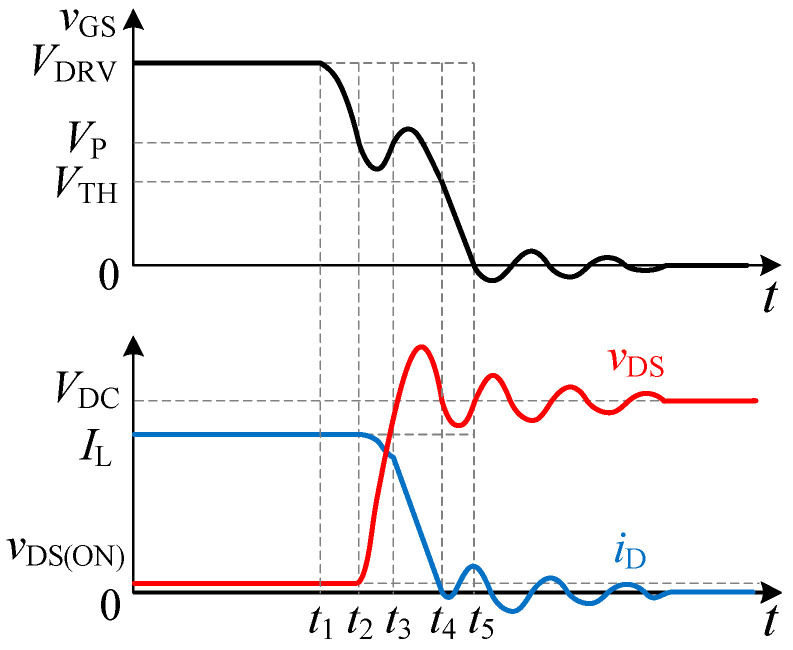 Figure 5
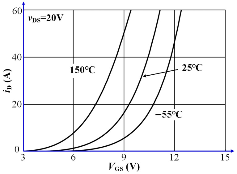 Figure 6
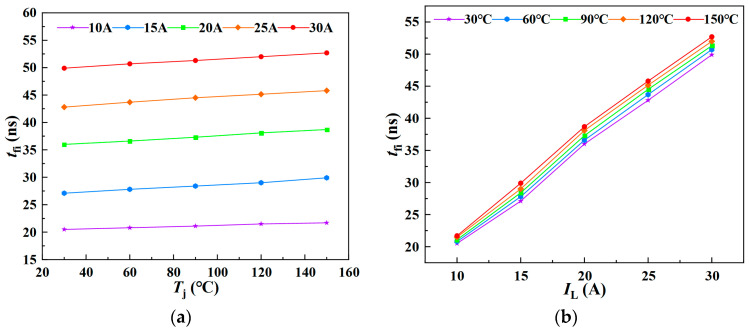 Figure 7
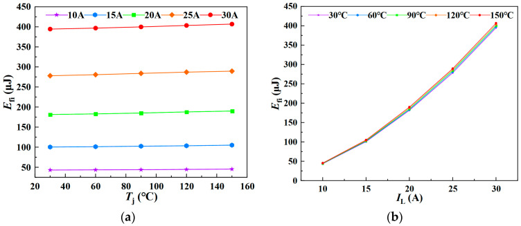 Figure 8
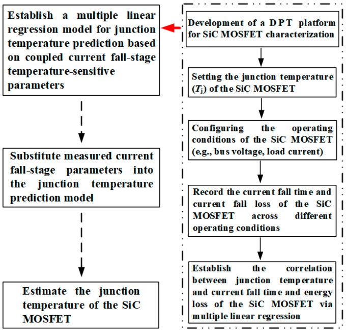 Figure 9
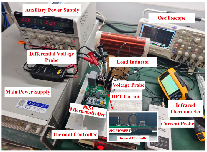 Figure 10
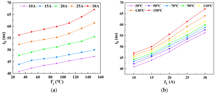 Figure 11
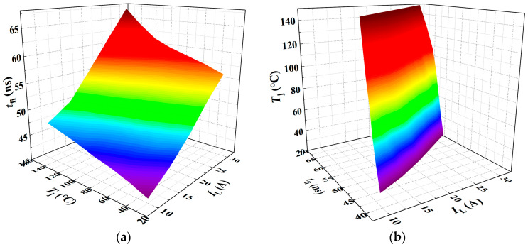 Figure 12
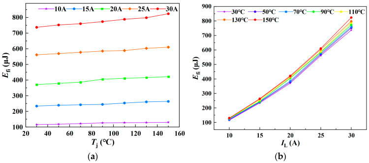 Figure 13
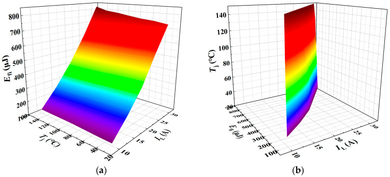 Figure 14
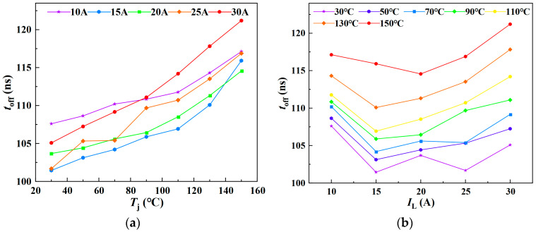 Figure 15
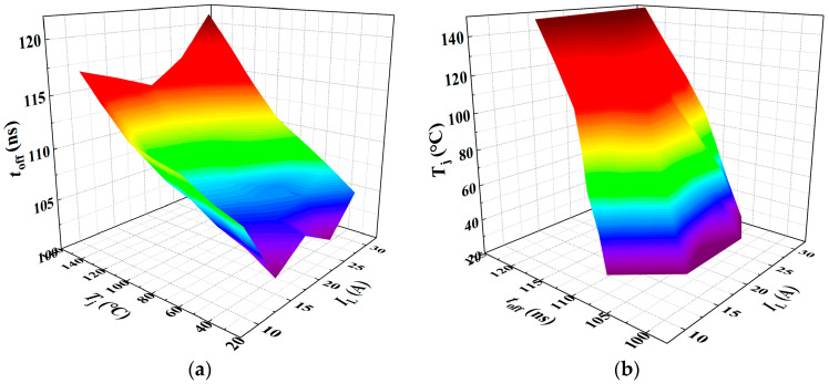 Figure 16
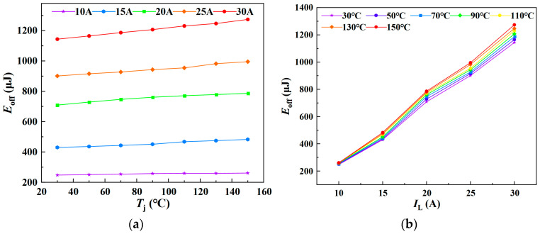 Figure 17
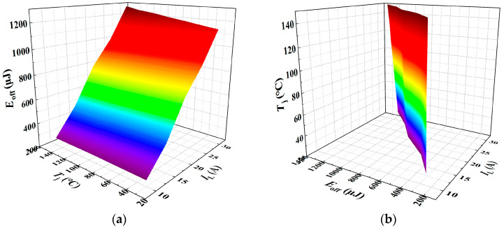 Figure 18
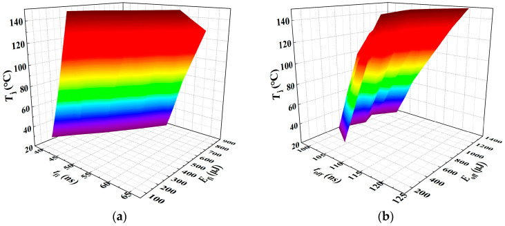 Figure 19
- —Aeronautical Science Foundation of China
Peer Reviews
No public reviews on file for this paper yet. If you reviewed it on a platform where reviews are public (OpenReview, ICLR, NeurIPS, ICML), you can paste yours below so the community can read it here.
Videos
No videos yet. Explain this paper in a talk, walkthrough, or lecture? Add one.
Taxonomy
TopicsSilicon Carbide Semiconductor Technologies · Advancements in Semiconductor Devices and Circuit Design · Semiconductor materials and devices
1. Introduction
Silicon carbide power devices offer advantages such as high-power density [1], excellent high-temperature tolerance, low on-state resistance [2], and high switching frequency [3], making them well-suited for high-power-density power electronics systems. In recent years, they have been increasingly adopted in applications such as rail transportation, aerospace, and wind energy conversion systems [4].
As SiC power device technology continues to mature, reliability concerns in practical applications are becoming increasingly prominent [5]. Under typical operating conditions in power electronics systems, both the absolute junction temperature and its dynamic fluctuations are critical factors influencing device reliability.
Figure 1 illustrates the distribution of failure modes. Research shows that approximately 31% of power electronics system failures are attributed to power semiconductor device failures, with nearly 60% of these directly linked to thermal factors [6]. Thermal stress (including overheating and temperature fluctuations) is the primary cause of failure in power semiconductor devices, resulting in both transient failures (such as thermal breakdown, bond wire breakage, and solder melting) and aging failures (including bond wire fatigue and solder layer degradation) [7]. Furthermore, the failure rate of power semiconductors approximately doubles for every 10 °C increase in junction temperature [8]. These findings demonstrate the urgent need for effective junction temperature estimation techniques that not only support reliability assessments but also enable integration into practical thermal sensing systems for real-time device health monitoring.
Currently, the methods for measuring junction temperature in power MOSFETs can be broadly categorized into four types: physical contact methods based on sensors, optical methods, thermal resistance network model-based approaches, and temperature-sensitive electrical parameter methods [6]. The physical contact method is invasive and has a slow response time [9,10]; the optical method is limited in practical applications due to its high cost and difficulty in applying it to opaque packaging structures [11,12]. The thermal resistance network model-based approach is a commonly employed method for junction temperature estimation. However, it requires accurate measurement of the module case temperature and the development of a precise thermal resistance network model to be effective [13]. The accuracy of this method largely depends on the accuracy of the thermal impedance network model. Key thermal parameters necessary for constructing a high-precision model are often difficult to obtain, and the model accuracy is easily affected by device aging. Compared with the above three methods, the TSEP method has significant advantages such as fast response speed, high implementation feasibility, and high accuracy [14,15,16]. Commonly used temperature-sensitive electrical parameters (TSEPs) include on-state resistance or voltage drop, switching delay, leakage current, gate threshold voltage, and peak gate current, among others. Real-time tracking of junction temperature is achievable through the measurement of these indicators, and this method has demonstrated promising results, particularly in silicon (Si)-based devices [15,17,18,19].
However, for SiC MOSFETs, certain TSEP-based approaches often fail to deliver optimal monitoring performance and can be problematic for online implementation. First, the inherently high switching frequency of SiC MOSFETs complicates the precise measurement of switching delay indicators; second, due to their excellent high blocking capability, SiC MOSFETs exhibit extremely low leakage current at 25 °C (approximately 1 μA level), making precise measurement difficult [20]; third, although methods based on-state resistance remain applicable, their temperature sensitivity is relatively low (approximately 0.2 mΩ/°C), which limits their ability to meet high-accuracy requirements [21].
N. Baker et al. [22,23] employed the gate peak current as a TSEP, which can be obtained by measuring the voltage drop across the external gate drive resistor. However, this method is susceptible to measurement inaccuracies due to the influence of the gate drive circuit and varying operating conditions. Z. Zhang et al. [24] proposed an online monitoring method for junction temperature prediction based on the turn-off delay time of SiC MOSFETs. F. Yang et al. [25] utilized the turn-on delay time as a temperature-sensitive electrical parameter and further considered the impact of device aging on its effectiveness. However, the switching delay time of SiC MOSFETs exhibits inherently low temperature sensitivity, and, to enhance this sensitivity, both studies [24,25] employed relatively large gate drive resistances, which may in turn affect the device’s switching characteristics. Ying Wang et al. [26] proposed an online junction temperature prediction method based on the falling edge duration of the drain voltage, utilizing auxiliary circuitry to monitor the relevant characteristics of the drain voltage transient. However, this parameter is highly susceptible to measurement errors caused by the parasitic elements of the SiC MOSFET and requires high-precision instrumentation for accurate detection.
Previous studies have demonstrated that the voltage slew rate (dv/dt) and voltage rise time (trv) during the turn-off process are commonly employed for junction temperature estimation in IGBT devices. Lingfeng Shao et al. [27] proposed a hybrid model based on the voltage rise time and voltage rise loss (Erv) during the IGBT turn-off process. However, the turn-off characteristics are highly susceptible to variations in load conditions, which may compromise the accuracy of the junction temperature prediction model. Moreover, the applicability and temperature sensitivity characteristics of this method for SiC MOSFETs still require further experimental validation.
To address the issue of insufficient temperature sensitivity in the switching characteristics of SiC MOSFETs and the difficulty of accurately predicting junction temperature using traditional single TSEPs, this paper proposes an MLR method for junction temperature estimation based on tfi and Efi. This method is designed not only to improve estimation accuracy but also to enable practical integration into temperature-sensing systems for real-time thermal monitoring of power semiconductor devices. The structure of this paper is as follows: Section 2 first establishes a mathematical model for the current fall stage of SiC MOSFETs, theoretically derives the temperature-sensitive characteristics of tfi and Efi during the current fall stage, and verifies these characteristics through simulation; Section 3 details the construction method and process of the MLR junction temperature prediction model based on tfi and Efi; Section 4 conducts experimental research using a double-pulse test (DPT) platform, in which both the turn-off characteristics and current fall phase parameters of SiC MOSFETs are measured, and corresponding MLR models are then constructed for comparison and validation. Experimental results demonstrate the accuracy and effectiveness of this junction temperature prediction method; and Section 5 summarizes the key findings and concludes this paper. This work provides a promising foundation for the development of compact, low-cost junction temperature sensors based on SiC MOSFETs.
2. Analysis of the Temperature-Dependent Characteristics of Parameters During the Current Fall Phase
2.1. Structure and Equivalent Circuit Model of SiC MOSFETs
Taking a SiC MOSFET packaged in a TO-247-3L package as an example, the internal structure diagram and the corresponding equivalent circuit of the discrete device are presented in Figure 2. As shown in Figure 2a, the TO-247-3L is one of the most commonly used discrete packaging structures for SiC MOSFETs. In this package, the drain terminal on the backside of the chip is connected to the lead frame through a solder layer, while the gate and source terminals on the front side are connected to their respective leads via aluminum bond wires. The entire assembly is then encapsulated in a plastic molding compound. However, due to the use of metal bond wires and a planar chip layout, the current path from drain to source is relatively long. As a result, the parasitic inductances associated with the internal package and external leads become non-negligible and can significantly influence the device’s high-speed switching performance.
Figure 2b illustrates the equivalent circuit diagram corresponding to the parasitic inductance components of the TO-247-3L package shown in Figure 2a. In this diagram, G, D, and S denote the intrinsic gate, drain, and source terminals of the SiC MOSFET die. The nodes labeled g, d, and s represent the gate, drain, and source terminals after accounting for the internal bonding wires. The nodes g′, d′, and s′ further represent the respective terminals after incorporating both the internal bonding wire inductance and the parasitic inductance introduced by the external package leads. LG(int), LD(int), and LS(int) represent the equivalent parasitic inductances of the internal bonding wires within the device package, while LG(ext), LD(ext), and LS(ext) denote the equivalent parasitic inductances associated with the external package leads and PCB trace connections.
Figure 3 presents the double-pulse test circuit for SiC MOSFETs, incorporating the key parasitic parameters. In Figure 3, VDC represents an ideal voltage source equivalent to the DC bus; IL denotes an ideal current source equivalent to the load inductance; CL accounts for the parasitic capacitance associated with the load inductance; D_H_ is an ideal SiC Schottky Barrier Diode (SBD); CJ represents the equivalent junction capacitance of the SiC SBD; CGS, CGD, and CDS represent the gate-to-source, gate-to-drain, and drain-to-source capacitances of the SiC MOSFET, respectively; LD(int) and LS(int) denote the parasitic inductances associated with the drain and source terminals introduced by the device packaging; RG(int) is the intrinsic gate resistance of the SiC MOSFET; RG(ext) represents the external gate drive resistance; LG represents the parasitic inductance of the gate loop; LD(ext) and Rloop denote the equivalent parasitic inductance and stray resistance, respectively, in the conduction path from the positive terminal of the DC bus to the drain terminal of the SiC MOSFET; and LS(ext) corresponds to the parasitic inductance in the return path from the source terminal of the SiC MOSFET to ground.
Figure 3 provides a detailed depiction of the parasitic parameters associated with each component, along with clearly defined current flow directions. Here, iD denotes the drain current, iG represents the gate current, and iGS, iGD, and iDS represent the displacement currents through CGS, CGD, and CDS, respectively. iCH refers to the channel current of the SiC MOSFET, and IL is the load current.
2.2. Modeling of the Drain Current Fall Phase
Figure 4 presents the equivalent circuit for the drain current fall phase (t3–t4) under double-pulse testing. The corresponding experimental turn-off waveforms of the SiC MOSFET are depicted in Figure 5. At time t3, the drain voltage clamps to the bus voltage, preventing further rise. Consequently, the gate-source voltage begins to decrease. With the MOSFET operating in the saturation region, the drain current commences its decay. Simultaneously, the load current commences commutation to the freewheeling diode until iD reaches zero. Throughout this interval, vGS continues to fall towards the threshold voltage VTH, governed by the expression:
Since the gate current iG is significantly smaller than the drain current iD, it is neglected in the derivation of the circuit equations.
By combining the above equations, the governing equation for this stage is obtained:
The expression for the drain current fall rate is derived as follows:
The expression for the drain current iD during the interval t3 to t4 is derived as follows:
The duration of this interval is then calculated as follows:
The power dissipation during this switching phase is given by the following:
2.3. Temperature-Dependent Characteristics Analysis of tfi and Efi During the Current Fall Phase
The transfer characteristics of a SiC MOSFET describe the relationship between the drain current and the gate-source voltage. This relationship is typically represented by a transfer characteristic curve, whose slope corresponds to the device’s transconductance. A steeper slope indicates higher transconductance, reflecting greater sensitivity of the drain current to changes in gate voltage. Figure 6 presents the transfer characteristic curves of the SiC MOSFET model NTHL020N090SC1 from the ON Semiconductor. Within a certain range, the slope of the curve increases with the gate-source voltage, indicating enhanced transconductance. A comparison of the curves at different temperatures reveals that, with rising temperature, the entire transfer curve shifts upward, and the threshold voltage decreases progressively. This indicates that higher temperatures facilitate device turn-on, as a lower gate voltage is required to achieve the same drain current.
The transfer characteristic curve illustrates the relationship between the gate-source voltage vGS and the drain current iD under a constant drain-source voltage. The slope at each point on the curve reflects the device’s transconductance, which characterizes the amplification capability of the MOSFET. Among these parameters, the gate threshold voltage and transconductance are particularly significant in the output characteristics of SiC MOSFETs, both exhibiting strong temperature dependence. The threshold voltage can be expressed by Equation (11):
In this equation, ni denotes the intrinsic carrier concentration, while n and p represent the concentrations of electrons and holes, respectively. k is the Boltzmann constant, T is the absolute temperature in kelvins, NA is the acceptor doping concentration, εs is the relative permittivity of the semiconductor, COX is the characteristic capacitance of the oxide layer, and q is the unit charge. The intrinsic carrier concentration of SiC increases with temperature, and this rise predominantly influences the variation in the threshold voltage. As a result, the threshold voltage of SiC MOSFETs exhibits a negative temperature coefficient, decreasing as the temperature increases.
In the transfer characteristic curve of a MOSFET, the transconductance represents the ratio of the change in drain current iD to the change in gate-source voltage vGS, reflecting the degree to which the gate-source voltage controls the drain current. It can be mathematically expressed as shown in Equation (12):
In this equation, Z represents the channel width, μni denotes the electron mobility in the inversion channel, vGS is the gate-to-source voltage, and LCH represents the channel length. The electron mobility in the inverted channel, μni, can be expressed as a combination of several components derived from typical scattering mechanisms, including bulk lattice scattering (μB), surface roughness scattering (μsr), surface phonon scattering (μph), and interface state scattering (μit):
The inversion channel electron mobility of SiC MOSFETs increases with temperature up to approximately 600 K [28]. On the other hand, the threshold voltage of SiC MOSFETs decreases with rising temperature, so the transconductance of SiC MOSFETs increases with rising temperature.
Based on the analysis and modeling of the current fall phase, the duration of this phase can be expressed as follows:
By differentiating the current fall time with respect to the junction temperature Tj, the following expression is obtained:
Based on the above analysis, it can be concluded that the transconductance gfs exhibits a positive temperature coefficient, whereas the threshold voltage VTH exhibits a negative temperature coefficient. Therefore, the following relationship can be derived:
Therefore, the current fall time during the turn-off process exhibits a positive temperature coefficient, indicating that the current fall duration of the SiC MOSFET increases progressively with rising temperature.
The energy loss during the current fall phase can be expressed as follows:
Similarly, differentiating the energy loss Efi during the current fall phase with respect to the junction temperature Tj yields the following:
From the above analysis, the transconductance gfs exhibits a positive temperature coefficient, while the threshold voltage VTH shows a negative temperature coefficient. As a result, the derivative of Efi with respect to junction temperature Tj is positive, dEfi/dTj > 0.
Therefore, the energy loss during the current fall stage of the turn-off process exhibits a positive temperature coefficient, indicating that the current fall energy loss of the SiC MOSFET increases progressively with rising junction temperature.
From the above analysis, it can be seen that, during the turn-off process, the current fall time and current fall loss both increase with the rise in junction temperature, exhibiting a positive correlation with junction temperature.
2.4. Simulation Analysis of Temperature-Dependent Characteristics
Based on the above analysis, it can be concluded that the parameter characteristics during the current fall stage of SiC MOSFETs in practical circuit applications are significantly influenced by the junction temperature and exhibit a monotonic trend with temperature variation. These characteristics can therefore serve as TSEPs for predicting the junction temperature of SiC MOSFETs.
This section presents simulation results conducted using LTspice software XVII. The parasitic inductance parameters of both the power and gate drive circuits are treated as adjustable variables, while all other parameters are set according to actual operating conditions. The simulations aim to verify the impact of varying junction temperatures on the current fall time and current fall loss. The detailed parameters of the SiC MOSFET double-pulse test circuit used in the simulation are summarized in Table 1.
A double-pulse simulation circuit was implemented in LTspice XVII, with the device model’s junction temperature set at five discrete levels: 30 °C, 60 °C, 90 °C, 120 °C, and 150 °C. The current fall time tfi and current fall loss Efi parameters were extracted and recorded from the simulation results. Figure 7 presents the simulated relationships among junction temperature, load current, and current fall time during the turn-off process of the SiC MOSFET. The results align well with the theoretical analysis, demonstrating that the current fall time increases with both rising junction temperature and load current during turn-off.
Figure 8 illustrates the simulated relationship between junction temperature, load current, and current fall energy loss during the turn-off process. The simulation results are consistent with the theoretical analysis, indicating that the current fall energy loss increases with both higher junction temperatures and greater load currents.
Based on the above simulation analysis, it can be observed that, during the current fall phase of the SiC MOSFET turn-off process, both the current fall time tfi and the associated energy loss Efi increase with rising junction temperature. The simulation results further demonstrate that tfi and Efi exhibit a linear correlation with Tj, effectively reflecting the junction temperature variations in the SiC MOSFET.
Based on the aforementioned theoretical and simulation analyses, it can be concluded that both tfi and Efi exhibit a positive correlation with junction temperature during the turn-off process of the SiC MOSFET. This confirms their feasibility as TSEPs. Accordingly, this paper proposes an MLR approach to estimate the junction temperature based on tfi and Efi.
3. Junction Temperature Estimation Method Based on MLR During the Current Fall Phase of SiC MOSFETs
Through experimental testing on a calibration platform, temperature-sensitive electrical parameter data under various operating conditions and junction temperatures can be obtained. By fitting a three-dimensional surface model involving current fall time tfi, current fall energy loss Efi, load current IL, and junction temperature Tj, MLR models for tfi-Tj-IL and Efi-Tj-IL relationships can be established, as expressed in Equations (19) and (20):
The general form of the multiple linear regression model is defined as shown in Equation (21):
This equation defines the structure of a multiple linear regression model. In this context, Y denotes the dependent variable, while X1, X2, ..., Xm represent the independent variables. The partial regression coefficients βj (j = 1, 2, ..., m) represent the average change in Y when Xj increases or decreases by one unit while keeping the other independent variables constant.
Simulation results demonstrate that the TSEPs increase with rising junction temperature Tj and load current IL. In this context, tfi and Efi serve as dependent variables, while Tj and IL are considered independent variables. Accordingly, a multiple linear regression model was established to describe the relationship between the temperature-sensitive parameters and the junction temperature and load current. However, for the purpose of junction temperature prediction, it is essential to construct a regression model in which Tj is the dependent variable and the remaining parameters serve as independent variables, as expressed in Equation (22).
However, since there is no direct linear causal relationship between IL and Tj in this model, the fitting accuracy is limited, and the explanatory power for the dependent variable is relatively weak. Therefore, it is necessary to eliminate the influence of load current to improve the accuracy of the temperature-sensitive electrical parameter method when applied to junction temperature prediction of SiC MOSFETs. By coupling multiple TSEPs, the effect of load current can be eliminated through matrix operations, enabling the extraction of the junction temperature. The implementation process is as follows:
Then, the following expression can be obtained:
An MLR model for predicting the junction temperature of Tj-tfi-Efi was established based on the three-dimensional data of tfi-Tj-IL and Efi-Tj-IL. By incorporating multiple TSEPs, the influence of load current IL was effectively decoupled, thereby enhancing the accuracy of junction temperature estimation for SiC MOSFETs using electrical parameter-based methods.
Therefore, an MLR method for junction temperature prediction based on the current fall characteristics of SiC MOSFETs is proposed, as illustrated in Figure 9. Initially, a DPT platform was established to facilitate model construction. To ensure that the parasitic parameters in the calibration setup closely match those in the actual operating circuit, both circuits should be designed with similar structural configurations and PCB layouts.
Experimental validation was performed using a DPT platform, with an oscilloscope employed to capture the temperature-dependent characteristics of the current fall phase during the turn-off process. The operating conditions for the SiC MOSFET were set, including the junction temperature Tj, DC bus voltage, and load current. The junction temperature was controlled via an intelligent temperature regulation unit. The tfi and Efi of the SiC MOSFET during the turn-off process were measured under various operating conditions and different junction temperatures. The relationship between junction temperature and TSEPs was fitted using MATLAB R2023b or Origin 2021 software. Based on the coupling of multiple TSEPs in the current fall phase, an MLR model was established to predict the junction temperature of the SiC MOSFET. Finally, by substituting the measured values of tfi and Efi into the established Tj-tfi-Efi junction temperature prediction model, the junction temperature Tj of the SiC MOSFET can be accurately estimated. This implementation not only enhances temperature estimation accuracy but also provides a practical foundation for developing compact, real-time junction temperature sensing solutions in SiC-based power electronic systems.
4. Experimental Validation
4.1. Experimental Platform
Figure 10 illustrates the DPT platform developed in this study for characterizing SiC MOSFETs. The main components of the platform include the following: (1) an intelligent temperature control chamber; (2) the DPT circuit; (3) a high-power DC power supply; (4) an infrared thermometer; (5) auxiliary power supplies; (6) high-voltage differential probes and high-bandwidth current probes; (7) a digital storage oscilloscope; and (8) load inductor.
The NTHL020N090SC1 SiC MOSFET was selected as the device under test (DUT). The DUT was mounted on a temperature-controlled heating stage equipped with an insulation pad. The stage temperature was varied from 30 °C to 150 °C in 20 °C increments (30 °C, 50 °C, 70 °C, 90 °C, 110 °C, 130 °C, 150 °C). At each temperature, the DUT was allowed to thermally stabilize for 5 min prior to measurement. Switching characteristics were then measured at load currents ranging from 10 A to 30 A in 5 A steps.
A constant-temperature heating duration of 5 min ensures sufficient thermal conduction within the chip, allowing the case temperature (Tc) and junction temperature Tj of the device to closely approximate the set temperature of the heating platform. Furthermore, to minimize the influence of self-heating during the calibration process, each pulse signal is limited to only a few microseconds. The heat generated by the chip during this extremely short period is negligible and does not significantly affect the junction temperature. Once the MOSFET chip reaches the target temperature, the corresponding voltage and current waveforms are captured using a digital oscilloscope, and the measurement data are subsequently recorded for analysis.
In addition, the platform adopts the same gate driver circuit design as that used in actual power electronic converters and allows configurable experimental conditions to emulate real operating points. This ensures that the switching characteristics obtained from experiments essentially reflect the behavior of the device under test within practical converters under identical driving conditions, thereby maximizing the comparability of the extracted parameters and the relevance of the model calibration data. This experimental consistency also enhances the applicability of the proposed method for integration into embedded temperature-sensing systems, where the extracted TSEPs can serve as internal indicators for real-time junction temperature monitoring without requiring additional temperature sensors or circuitry. Table 2 presents the operating conditions of the SiC MOSFET double-pulse test platform.
4.2. Experimental Results and Analysis
As illustrated in Figure 11a,b, the variation of tfi with junction temperature under different load currents and its variation with load current at different junction temperatures are depicted, respectively. The experimental results demonstrate that the current fall time during the turn-off phase increases approximately linearly with both rising junction temperature and load current. Based on these observations, a multiple linear regression model for tfi-Tj-IL can be established.
As shown in Figure 12, a three-dimensional surface model of tfi-Tj-IL is constructed and fitted using Matlab R2023b/Origin 2021 software based on multiple linear regression.
When tfi is treated as the dependent variable, the resulting regression model is expressed in Equation (26), with a goodness of fit R^2^ of 98.08%. Conversely, when Tj is taken as the dependent variable, the corresponding regression model is given in Equation (27), with an R^2^ value of 88.88%.
Similarly, Efi was measured under varying junction temperatures and load currents, with the experimental results presented in Figure 13. Figure 13a,b illustrate the variation of Efi with junction temperature at different load currents, and with load current at different junction temperatures, respectively. The results indicate that the current fall loss during the turn-off phase increases approximately linearly with both junction temperature and load current. Accordingly, a multiple linear regression model for Efi as a function of Tj and IL was established.
As illustrated in Figure 14, the three-dimensional surface model of Efi with respect to Tj and IL is presented.
A multiple linear regression model was fitted using Matlab R2023b/Origin 2021 software. When Efi is treated as the dependent variable, the resulting regression model is given in Equation (28), yielding a goodness of fit R^2^ of 99.04%. Conversely, when Tj is taken as the dependent variable, the corresponding regression model is shown in Equation (29), with a significantly lower goodness of fit R^2^ of only 28.91%.
The multiple linear regression models derived from fitting the tfi-Tj-IL and Efi-Tj-IL datasets indicate that both tfi and Efi increase linearly with rising junction temperature and load current. These models, with tfi and Efi as dependent variables and Tj and IL as independent variables, demonstrate a high goodness of fit, effectively capturing the temperature- and current-dependent variations in the electrical parameters. However, the fitted MLR models exhibit varying degrees of goodness of fit. The R^2^ value for the Tj-IL-tfi three-dimensional model is 88.88%, whereas that for the Tj-IL-Efi model is only 28.91%. Therefore, relying on a single temperature-sensitive electrical parameter to estimate the junction temperature may introduce substantial errors, resulting in reduced prediction accuracy.
Since switching losses in SiC MOSFETs primarily occur during the voltage rise and current fall intervals of the turn-off process, the total energy dissipated in these intervals is defined as the turn-off loss Eoff, and the corresponding duration is defined as the turn-off time toff. In the following sections, three-dimensional models of toff and Eoff are established, followed by the development of a junction temperature prediction model. A comparative analysis of their performance is also presented.
As shown in Figure 15a,b, the variations of toff with junction temperature under different load currents, and with load current under different junction temperatures, are presented, respectively. The experimental results indicate that the turn-off time increases approximately linearly with increasing junction temperature. Figure 16 presents the three-dimensional surface model of toff-Tj-IL. When toff is treated as the dependent variable, the corresponding multiple linear regression model is given in Equation (30), yielding a goodness of fit R^2^ of 73.85%. Conversely, when Tj is considered the dependent variable, the fitted model is shown in Equation (31), with an R^2^ value of 73.53%.
Similarly, Eoff was characterized under various junction temperatures and load currents, with the experimental results presented in Figure 17. Figure 17a,b, respectively, illustrate the variation of Eoff with junction temperature under different load currents, and the variation of Eoff with load current under different junction temperatures. The experimental results indicate that the current fall time during the turn-off process increases approximately linearly with both junction temperature and load current. Figure 18 presents the three-dimensional surface model of Eoff-Tj-IL. When Eoff is treated as the dependent variable, the fitted multiple linear regression model is presented in Equation (32), yielding a goodness of fit R^2^ of 99.43%. When Tj is considered the dependent variable, the corresponding regression model is shown in Equation (33), with a goodness of fit of 45.95%.
The fitted multiple linear regression models of toff-Tj-IL and Eoff-Tj-IL indicate that both toff and Eoff exhibit an approximately linear increase with rising junction temperature. The regression models established with toff and Eoff as dependent variables and Tj and IL as independent variables demonstrate a high goodness of fit, effectively capturing the variations in TSEPs induced by changes in junction temperature and load current. However, when Tj is treated as the dependent variable, the goodness of fit of the regression models is relatively low. Specifically, the goodness of fit R^2^ for the Tj-IL-toff model is 73.85%, while that for the Tj-IL-Eoff model is only 45.95%.
Based on the fitting results of the junction temperature prediction models developed for the turn-off process and the current fall stage using TSEPs, it is evident that models relying on a single temperature-sensitive electrical parameter to back-calculate the junction temperature from operating conditions exhibit limited goodness of fit and poor prediction accuracy. To eliminate the influence of load current on junction temperature prediction, multiple TSEPs were coupled in the multiple linear regression model. Figure 19 presents the Tj-tfi-Efi and Tj-toff-Eoff three-dimensional models, respectively.
These models incorporate the TSEPs from the current fall stage and the turn-off process to construct and fit improved junction temperature prediction models. When junction temperature Tj is used as the dependent variable, and tfi and Efi are the independent variables, the resulting multiple linear regression model is presented in Equation (34), yielding a goodness of fit R^2^ of 94.11%. Similarly, when Tj is modeled as a function of toff and Eoff, the corresponding regression model is given in Equation (35), with a goodness of fit R^2^ of 75.41%.
The goodness of fit comparison of the temperature prediction models established using a single temperature-sensitive electrical parameter and multiple linear regression based on coupled TSEPs is shown in Table 3.
As shown in the comparison results of the fitting accuracy of the three-dimensional model of TSEPs in Table 2, the proposed multiple linear regression method for junction temperature prediction based on the current fall phase characteristics of SiC MOSFETs demonstrates high accuracy, with an improvement of 5.23% compared to using the single temperature-sensitive electrical parameter tfi. Furthermore, coupling temperature-sensitive parameters from the turn-off process also enhances prediction accuracy relative to single-parameter models, thereby confirming the effectiveness and feasibility of the selected parameters. Additionally, comparison of the experimental results reveals that, for a junction temperature prediction model based on multiple TSEPs, its prediction accuracy depends on the combined contribution of each TSEP. The greater the temperature sensitivity of the individual TSEPs, the higher the prediction accuracy achieved by their coupled junction temperature model. Specifically, the Tj-tfi-Efi junction temperature prediction model established using coupled TSEPs from the current fall phase achieves higher accuracy than the Tj-toff-Eoff model based on the turn-off process, indicating its greater suitability for junction temperature estimation in SiC MOSFETs.
Table 4 presents a comparison of TSEPS for junction temperature measurement. Compared with other methods, the proposed approach exhibits better linearity and higher goodness of fit when applied to SiC MOSFETs. It requires no additional auxiliary circuitry, is well-suited for online monitoring, and does not interfere with the intrinsic characteristics of the circuit. Furthermore, the influence of load current is eliminated, thereby improving the accuracy of the temperature-sensitive electrical parameter-based junction temperature estimation model. These features not only validate the model’s estimation accuracy but also highlight its potential for integration into compact and low-cost embedded temperature-sensing systems for SiC-based power electronics.
5. Conclusions
This paper proposes an MLR method for junction temperature prediction based on the current fall characteristics of SiC MOSFETs. First, the feasibility of utilizing current fall time and current fall energy loss as TSEPs is demonstrated through theoretical analysis and simulation. Subsequently, an MLR junction temperature estimation model is constructed based on the three-dimensional mapping relationships between tfi-Tj-IL, Efi-Tj-IL, and Tj-tfi-Efi. Experimental results demonstrate that coupling the two TSEPs, tfi and Efi, effectively mitigates the influence of load current on model accuracy, thereby enhancing the precision of the MLR junction temperature prediction model. Compared to using tfi as the sole temperature-sensitive electrical parameter, the model accuracy improved by 5.23%. Additionally, compared to the Tj-toff-Eoff prediction model based on turn-off process characteristics, the proposed Tj-tfi-Efi model demonstrates superior suitability for junction temperature estimation in SiC MOSFETs. This study not only validates the feasibility and effectiveness of the proposed approach but also demonstrates its potential for practical deployment in compact, low-cost junction temperature sensing systems. The model’s non-intrusive nature and high accuracy make it well-suited for real-time thermal monitoring, health management, and reliability assessment in SiC-based power electronic applications.
The reference list from the paper itself. Each links out to its DOI / PubMed record.
- 1Yuan X. Laird I. Walder S. Opportunities, Challenges, and Potential Solutions in the Application of Fast-Switching Si C Power Devices and Converters IEEE Trans. Power Electron.2021363925394510.1109/TPEL.2020.3024862 · doi ↗
- 2Iannaccone G. Sbrana C. Morelli I. Strangio S. Power Electronics Based on Wide-Bandgap Semiconductors: Opportunities and Challenges IEEE Access.2021913944613945610.1109/ACCESS.2021.3118897 · doi ↗
- 3She X. Huang A.Q. LucíaÓ. Ozpineci B. Review of Silicon Carbide Power Devices and Their Applications IEEE Trans. Ind. Electron.2017648193820510.1109/TIE.2017.2652401 · doi ↗
- 4Zhu Z. Zhao Y. Yan W. Behavioral Modeling of Si C MOSFET Static and Dynamic Characteristics Based on Particle Swarm Optimization Algorithm IEEE Access.202513669946700510.1109/ACCESS.2025.3542060 · doi ↗
- 5Sun P. Guo Y. Wu T. Zhao Z. Lai P. Chen Z. An Online Junction Temperature Monitoring Correction Method for Si C MOSFE Ts at Different Parasitic Parameters IEEE J. Emerg. Sel. Top. Power Electron.2022105007501810.1109/JESTPE.2021.3117734 · doi ↗
- 6Lu X. Wang L. Yang Q. Yang F. Gan Y. Zhang H. Investigation and Comparison of Temperature-Sensitive Electrical Parameters of Si C mosfet at Extremely High Temperatures IEEE Trans. Power Electron.2023389660967210.1109/TPEL.2023.3267472 · doi ↗
- 7Wang B. Cai J. Du X. Zhou L. Review of power semiconductor device reliability for power converters CPSS Trans. Power Electron. Appl.2017210111710.24295/CPSSTPEA.2017.00011 · doi ↗
- 8Alatise O. Parker-Allotey N.-A. Mawby P. Modeling the Electrothermal Stability of Power MOSFE Ts During Switching Transients IEEE Electron Device Lett.2012331039104110.1109/LED.2012.2196671 · doi ↗