2D Atomic Templating for the Large-Scale Synthesis of Metastable CuInS2 and Its Heterojunctions
Jui-Teng Chang, Yu-Xiang Chen, Hao-Ting Chin, Ding-Rui Chen, Jian-Jhang Lee, Chia-Yi Wu, Yi-Chia Chou, Mario Hofmann, Ya-Ping Hsieh

TL;DR
A new method for making high-quality CuInS2 material is developed, enabling better performance in energy technologies.
Contribution
A novel atomic templating strategy enables large-scale synthesis of phase-pure CuInS2 and its heterojunctions.
Findings
The atomic templating method produces phase-pure wurtzite CuAu-type CuInS2.
The synthesis mechanism involves strain-mediated cation exchange for precise control.
The approach enables scalable growth of 2D heterojunctions with improved optoelectronic and thermoelectric performance.
Abstract
CuInS2 has emerged as a promising material for sustainable energy technologies due to its combination of attractive electronic, economic, and ecological properties. However, current synthesis routes exhibit limited phase uniformity and degraded optoelectronic performance due to the complex Cu–In–S phase diagram. In this work, we report a synthesis strategy that overcomes these limitations and can produce CuInS2 with a singular crystalline phase. An atomic templating approach is described that retains the structural order of a two-dimensional (2D) transition-metal monochalcogenide host to realize phase-pure wurtzite CuAu-type CuInS2. Structural and spectroscopic characterization confirms the exclusive formation of this metastable phase and provides insights into its electronic properties. The transformation proceeds via a strain-mediated layer-by-layer cation-exchange mechanism, enabling…
Genes, proteins, chemicals, diseases, species, mutations and cell lines named across the full text — each resolved to its canonical identifier and authoritative record.
Click any figure to enlarge with its caption.
 1
1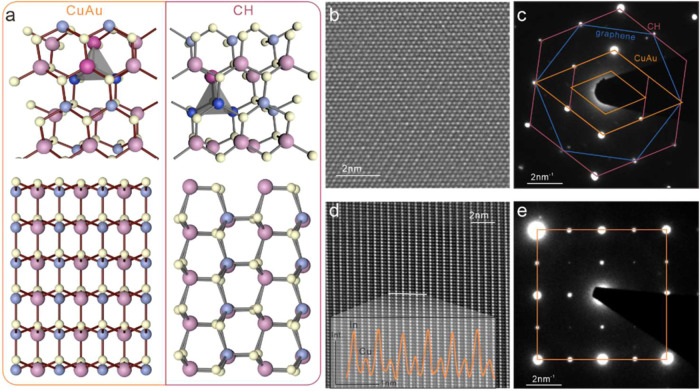 2
2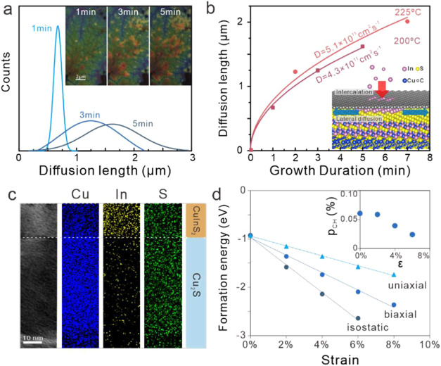 3
3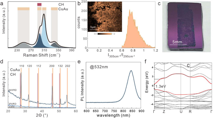 4
4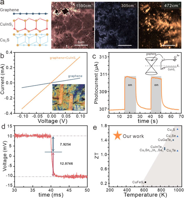 5
5- —Academia Sinica10.13039/501100001869
- —Ministry of Science and Technology, Taiwan10.13039/501100004663
- —Ministry of Science and Technology, Taiwan10.13039/501100004663
- —Ministry of Science and Technology, Taiwan10.13039/501100004663
- —Ministry of Science and Technology, Taiwan10.13039/501100004663
- —National Taiwan University10.13039/501100006477
Peer Reviews
No public reviews on file for this paper yet. If you reviewed it on a platform where reviews are public (OpenReview, ICLR, NeurIPS, ICML), you can paste yours below so the community can read it here.
Videos
No videos yet. Explain this paper in a talk, walkthrough, or lecture? Add one.
Taxonomy
Topics2D Materials and Applications · Quantum Dots Synthesis And Properties · Advanced Photocatalysis Techniques
Introduction
1
CuInS_2_ is an enabling material for sustainable energy applications due to its combination of favorable electronic, economical, and ecological properties. First, the material boasts a high absorption coefficient,? optimal band gap, and a long carrier lifetime? that make it promising for high-performance solar energy harvesting.? Moreover, its energy levels are well aligned with the requirements for photocatalytic hydrogen production.? Finally, its utilization of nontoxic and low-cost constituents? permits the scaling of the envisioned energy generation devices to industrial relevant dimensions.
Current synthesis methods, however, face significant challenges in achieving sufficiently large and controllable production, thereby limiting the material’s applicability in the envisioned green energy devices. Traditional synthesis approaches, including solution processing, colloidal synthesis, and solid-state reactions, often yield nanocrystals with exceptional properties but on a small scale.? When these nanostructures are integrated into macroscopic devices, their performance degrades due to surface scattering and structural inconsistencies.?
Thin film techniques such as sputtering and chemical vapor deposition offer the ability to produce large-scale devices, but they encounter unique challenges specific to CuInS_2_: Due to the complex phase diagram, CuInS_2_ films suffer from the coexistence of multiple crystalline phases.? The resulting mixture of domains produces disorder and non-radiative recombination pathways that compromise the material’s overall performance.? Consequently, a new synthesis route is required that combines the phase stability of low-temperature, wet-chemical synthesis with the scalability of chemical vapor deposition.
In this work, we address these challenges by introducing a novel synthesis approach that yields CuInS_2_ with a singular crystalline phase at the macroscopic scale. We devised an atomic templating strategy that converts a 2D material into CuInS_2_ while retaining the atomic structure imposed by the host. The atomic conversion of a recently discovered transition-metal monochalcogenide? yields metastable wurtzite CuInS_2_ of CuAu type. Structural and spectroscopic analyses confirm the exclusive formation of the CuAu-type wurtzite phase, presenting the first opportunity to characterize its electronic structure. The atomic templating mechanism was elucidated, and a strain-mediated mechanism was proposed and corroborated through ab initio simulations. The layer-by-layer cation-exchange process opens up the unique ability to produce complex ternary 2D material vertical stacks at large scale and without interfacial contamination. We demonstrate the application of this multijunction synthesis process in optoelectronics and thermoelectric devices with high-performance metrics.
Results and Discussion
2
The crystalline structure of CuInS_2_ plays a significant role in its optoelectronic properties. A large portion of research has focused on the zincblende-type phase due to its thermodynamic stability.?
The CuInS_2_ phase diagram also contains a wurtzite structure that is only stable at elevated temperatures.? The wurtzite phase exhibits a smaller band gap at 1.47 eV and a pronounced pressure tunability of its electronic structure,? which could make it the more attractive crystal phase for energy harvesting applications.
The integration of wurtzite CuInS_2_, however, has been limited due to challenges in its synthesis, as conventional synthesis processes exhibit uncontrollable mixtures of both phases. These issues in producing wurtzite CuInS_2_ are due to the small energy differences between the different phases and subphases, resulting in low selectivity.? Consequently, only nanocrystals with phase mixtures have been realized to date.?
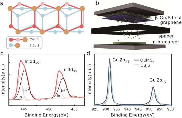
To overcome these issues, we pursue an atomic templating process, where a host crystal is modified through the exchange of its constituents. Ion exchange in nanocrystals has demonstrated the impact of the host crystal’s structure on the resulting target crystal.? We extend this concept by introducing 2D materials as hosts due to their known structural robustness? and the demonstrated uniform crystallinity over wafer scale.? The ideal host crystal for wurtzite CuInS_2_ is found to be the 2D transition-metal monochalcogenide β-Cu_2_S. Crystallographic analysis demonstrates that the anion lattice of β-Cu_2_S shows a one-to-one correspondence with the anion lattice of wurtzite CuInS_2_ (Figurea).
CuInS2 synthesis by atomic templating: (a) schematic of atomic templating of CuInS2 from β-Cu2S showing that the sulfur sublattices of both crystals are identical; (b) depiction of the synthesis process; (c) X-ray photoelectron spectrum of In 3d peak upon deposition, showing the contribution of surface-bound In and bonded In3+; and (d) Cu 2p peak showing a peak shift upon indium introduction.
While β-Cu_2_S is a metastable thermodynamic phase, it can be synthesized at large scale using a recently developed confined-reaction approach.? Briefly, graphene serves as a planarization layer that produces a van-der-Waals gap on the surface of a copper substrate. Gaseous sulfur intercalates into the van-der-Waals gap and stabilizes the uncommon hexagonal Cu_2_S phase. This graphene/Cu_2_S structure is transferred from the remaining Cu substrate to SiO_2_/Si substrate following previous reports.?
We subsequently transform β-Cu_2_S into CuInS_2_ by exposing it to In vapor. For this purpose, indium was deposited on a Si/SiO_2_ sample and then placed below the graphene/β-Cu_2_S sample with a graphite spacer (Figureb). The structure was heated under ambient pressure to 225 °C.
XPS characterization was employed to confirm the incorporation of In into the Cu_2_S lattice. First, the emergence of a sizable indium peak can be seen (Figurec). We furthermore observe that the Cu 2p peak shifts to lower binding energies compared to that of pristine Cu_2_S (Figured). This behavior agrees with predictions for the change in binding environments if In is introduced in the Cu_2_S lattice.? The retention of the narrow peak width provides a first indication of the uniformity of the binding environment and suggests that the substantial conversion of Cu_2_S into homogeneous CuInS_2_ occurs.
The conversion of Cu_2_S into CuInS_2_ is expected to yield wurtzite-type crystals due to their structural similarity to the Cu_2_S host crystal. However, wurtzite CuInS_2_ has two polytypes with similar formation energies:? the wurtzite-based CuAu phase (WZ-CuAu symmetry group Pmc21) represents a uniform distribution of Cu and In atoms. The wurtzite-based chalcopyrite (WZ-CH symmetry group: Pna21) shows disordered distributions of cations with either 3 copper or 3 indium atoms surrounding a sulfur site? (Figurea).
Characterization of the CuInS2 structure: (a) depiction of wurtzite chalcopyrite (WZ-CH) and wurtzite CuAu-type (WZ-CuAu) polytypes with indication of a tetragonal unit containing 2Cu (blue)/2In (pink) atoms for WZ-CuAu and 3Cu/1 In for WZ-CH (top) and sideview of both polytypes showing ordered arrangement of Cu (blue) and In(pink) columns for CuAu; (b) atomic-resolution HAADF STEM image of the basal plane; (c) corresponding selected area electron diffractogram (SAED) with the indication of lattices for graphene, WZ-CH, and WZ-CuAu; (d) HAADF STEM image of the cross-sectional plane showing a columnar arrangement of Cu and In, (inset) z-contrast cross section according to indicated line; and (e) corresponding SAED with the indication of the WZ-CuAu lattice.
To investigate the crystalline structure of the converted material, we conduct atomic-scale electron microscopy. For this purpose, the graphene/CuInS_2_ structure was transferred onto a transmission electron microscopy (TEM) grid. The basal plane exhibits a hexagonal structure (Figureb) that could originate from both wurtzite phases and the graphene layer. Selected area diffraction can help distinguish the graphene planarization layer from the crystal (Figurec). The remaining reflection spots can be assigned to both the hexagonal or orthorhombic crystal structure (Figurec). This ambiguity is due to the weakening of odd lattice reflexes in orthorhombic CuInS_2_ that is enhanced by its epitaxial ordering with graphene.?
In order to resolve this issue, we conducted cross-sectional TEM analysis. For this purpose, we converted thick Cu_2_S into CuInS_2_ and searched for folds after transfer. The annular dark-field transmission electron microscopy (ADF-TEM) image shows clear columns of bright and dark atoms when looking at the side of the CuInS_2_ crystal (Figured). This contrast is due to the different scattering efficiencies of heavy In and light Cu, allowing us to distinguish their locations (inset, Figured). This columnar arrangement of atoms agrees with the ac plane of CuAu-type wurtzite and provides clear evidence that wurtzite-type CuAu can be produced through atomic templating, despite its thermodynamic unfavorability. Electron diffraction of the ac plane further confirms the cubic arrangement that rules out the occurrence of the CH-type WZ structure.
To understand the process that leads to the formation of metastable CuInS_2_, we employed time-resolved growth studies, where the extent of CuInS_2_ regions in the Cu_2_S host crystal was analyzed after different growth durations. After short growth times, small grains of CuInS_2_ form within the Cu_2_S 2D material. These seeds are located at the boundaries of the host crystal (inset, Figurea). Within 5 min the grains grow and start coalescing into a continuous film.
Cation-exchange process: (a) distribution of distances between the converted material and boundary, (inset) optical micrographs of the converted material extent, as visually identifiable by bright regions, after different growth durations; (b) fit of the time-dependent average diffusion length to a diffusion model, (inset) schematic of the proposed cation-exchange mechanism; (c) cross-sectional micrograph of the converted material and the corresponding elemental mapping showing the uniform distribution of Cu and S and abrupt change of In composition; and (d) simulated formation energy per atom vs strain for different strain types in CuAu-type CuInS2, (inset) calculated occupation probality (pCH) of CH-WZ as a function of strain.
We quantify this observation by tracking the size of multiple grains over time. The distribution of grain sizes broadens with growth time (Figurea). This behavior suggests that the conversion process proceeds through diffusion, which is consistent with previously observed cation-exchange processes.? The time evolution of the mean grain size is fitted to a simple diffusion model that shows good agreement with the experimental data. We extract the diffusion coefficient by fitting and obtain a diffusion coefficient of D = 4.3 × 10^–11^ cm^2^ s^–1^. This value agrees well with the surface diffusion coefficient of Au atoms on graphene at the temperature (4.1 × 10^–11^ cm^2^ s^–1^).? From the increase in diffusion coefficient with temperature, we can extract an activation energy of approximately 100 meV. This low value rules out bulk cation transport in Cu_2_S as the rate-limiting step as it exhibits activation energies of ∼500 meV.? Instead, the value is comparable to expected diffusion energies of metals on graphene, which range from 10 meV for Ag to 166 meV for Al,? suggesting that surface diffusion is the controlling process.
Our observation that the templating process is surface-dominated is confirmed by cross-sectional TEM measurements, which show that thick Cu_2_S is retained even after 120 min of annealing and only a 40 nm surface layer is converted (Figurec). Moreover, different from lateral diffusion, the in-depth growth yields a sharp interface, as evidenced by compositional mapping (Figurec).
Based on these observations, we propose a strain-mediated cation-exchange mechanism (inset Figureb). Indium initially permeates the graphene layer through defects and edges to enter the van-der-Waals gap between graphene and Cu_2_S. To achieve the observed epitaxy with the graphene layer, CuInS_2_ has to sustain significant tensile strain. This behavior is corroborated by difference in lattice constants between our diffraction measurements and reported values as well as an upshift of Raman peaks compared to theoretical work as detailed below.? This large interfacial strain limits the motion of indium within the Cu_2_S lattice, and vertical diffusion is suppressed. Consequently, diffusion proceeds mainly parallel to the graphene and produces a planarized growth mode that yields sharp interfaces.?
This hypothesis is supported by ab initio simulations (Figured). We utilized LCAO-based density functional theory (DFT) to calculate the formation energy of CuInS_2_ through the exchange of Cu to In atoms in the original Cu_2_S structure. The formation energy is calculated according to
where the energies represent the total energies of atomic arrangements in the same unit cell and E In/E Cu represents the energies of bare In and Cu within the same unit cell, respectively. We observed that the deformation of the unit cell significantly decreases the formation energy, supporting our strain-mediated growth mechanism. Moreover, our simulations can also explain the observed selectivity toward CuAu-type wurtzite CuInS_2_. Straining increases the formation energy difference between the two crystal structures and thus decreases the probability of producing CH-type CuInS_2_ (inset, Figured). This explanation agrees with predictions of increased energy lowering by straining CuAu-type CuInS_2_ compared to CH due to their smaller Gruneisen parameter.?
The observed strain-mediated cationic-exchange mechanism is ideally suited to produce 2D CuInS_2_ that inherits the high crystalline quality and uniformity of the template.? We confirmed this feature by investigating the uniformity of the crystalline phase by spatially resolved Raman spectroscopy.
Due to the homogeneous unit cell, CuAu exhibits a more complex Raman response than chalcopyrite-type CuInS_2_. Indeed, we observe characteristic spectral features at 296 and 307 cm^–1^ that are consistent with f simulations for the LO and TO modes of the A1 symmetric vibration of the WZ-CuAu phase.? Moreover, additional peaks at 240 and 340 cm^–1^ have been previously observed for CuAu-type CuInS_2_ (Figurea).? Based on this analysis, the peak intensities around 305 and 295 cm^–1^ can serve as a descriptor of the distribution between CuAu and CH phases: the CH phase exhibits a single LO mode at 295 cm^–1^ but no TO mode, whereas the CuAu phase exhibits both peaks. Consequently, a low peak intensity ratio would correspond to the CH phase, whereas a higher value would represent the LO/TO distribution of WZ-CuAu. We observe a narrow distribution of the 305/295 cm^–1^ intensity ratio with a center of approximately 0.8 (Figureb). This value is in quantitative agreement with previous simulations of phase-pure CuAu-type,? indicating the uniform distribution of the material (Figurec).
Characterization of uniform CuAu-type CuInS2: (a) Raman spectrum with the indication of possible Raman modes for both wurtzite polytypes; (b) histogram of the intensity ratio I(ω = 305 cm–1)/I(ω = 295 cm–1) showing the prevalence of CuAu as described in the text, (inset) spatially resolved map of the intensity ratio; (c) photograph of the centimeter-scale sample showing contrast difference between the substrate (300 nm Si/SiO2) and grown material; (d) XRD characterization of the material and wafer using grazing angle XRD (GIXRD) and in-plane XRD (IPXRD) with assignment to CuAu modes and indication of possible CH modes; (e) photoluminescence spectrum of the material; and (f) DFT-calculated band structure of CuAu-type CuInS2 with the indication of the states closest to the Fermi level and their minimum separation.
This analysis is also supported by an X-ray diffraction analysis. The low thickness of the material makes grazing angle XRD (GIRXD) more effective than conventional XRD as seen in the higher signal-to-noise ratio of the obtained spectra (Figured). The peak assignment shows good agreement with predictions for the CuAu-type CuInS_2_ ? and a reasonable sharpness given the low thickness, which corroborates its high quality. More importantly, a potential co-occurrence of CH-type CuInS_2_ is ruled out as it would produce several overlapping features, but we do not see significant broadening compared to peaks that should not exhibit an overlap. This analysis corroborates our finding that uniform CuAu-type CuInS_2_ can be produced over large scale.
The new capability to produce homogeneous WZ-CuAu-type CuInS_2_ at centimeter dimensions (Figurec) permits us to investigate the properties of this metastable material. Previous reports suggested that the CuAu phase is metallic and shows no photoluminescence (PL).? However, our results clearly demonstrate the occurrence of a strong photoluminescence peak at 845 nm (Figuree). This result agrees with our DFT calculations that show a direct band gap at the Γ-point (Figuref).
Compared to conventional zincblende CuInS_2_, this new phase exhibits a smaller band gap, which enhances its suitability for electronic applications. This property, combined with the material’s scalability and uniformity, positions it as a promising candidate for next-generation optoelectronic devices.
In addition to enabling the realization of unstable thermodynamic phases, the atomic templating process exhibits another advantage. Recent research has demonstrated the promise of 2D material integration within van-der-Waals stacks. Those assemblies are produced by sequential mechanical transfer, which is highly complex and exhibits limited cleanliness and scalability.? Control of the cation-exchange process enables the direct growth of complex 2D material heterostructures. Through sequential growth, three different 2D materials could be stacked without any transfer step. First, graphene growth was conducted on copper foil, which can be achieved at commercially relevant scales and low costs.? In a second step, the graphene/Cu structure was exposed to sulfur to create Cu_2_S by van-der-Waals confined growth, leading to a high-quality graphene/Cu_2_S interface, as previously reported.? The third step represents cationic exchange to CuInS_2_ at a carefully controlled growth duration. This process utilizes the same reactor and can be carried out without breaking vacuum. This direct-growth approach of ternary 2D heterojunctions increases their simplicity, scalability, and commercial appeal. Moreover, the interfaces between the constituents occur through self-organization, which alleviates concerns of contamination.
To illustrate this concept, we demonstrate multispectral Raman maps. Within the same location, the response of CuInS_2_, Cu_2_S, and graphene was characterized (Figurea). We find that all materials are continuous. The relative prevalence of Cu_2_S depends on the initial morphology and the processing duration, and we chose a condition that retains large areas of this material in the heterojunction.
Formation and application of heterostructures: (a) collocated Raman maps of spectral features corresponding to graphene (1590 cm–1), CuInS2 (305 cm–1), and Cu2S (472 cm–1) that demonstrate the morphology of the graphene planarization layer, the CuInS2 middle layer, and the Cu2S bottom; (b) current–voltage characteristics of bare graphene device and heterostructure device, (inset) false color optical micrograph of the device; (c) time evolution of the device current under toggled illumination, (inset) schematic of the photoexcited carrier recombination pathway; (d) Harman measurement with the indication of thermal and ohmic voltage components; and (e) comparison of the extracted ZT value with literature values (list in the Supporting Information).
To characterize the resulting triple heterojunction, we conduct carrier transport measurements in a lateral geometry (inset of Figureb). We observe that the conductivity of the heterojunction assembly is enhanced over that of the bare graphene control device (Figureb). This observation suggests that conduction proceeds efficiently across the heterojunction interfaces and that the underlying layers can assist in the conduction.?
We further confirm efficient vertical carrier transport within the heterostructure through optical measurements. For this purpose, a 405 nm laser was toggled on the device and the device current was recorded (Figurec). We see that the photocurrent is only 13% of the dark current, which indicates that photoexcited carriers quickly recombine in the graphene (inset, Figurec).
The observed low injection barrier in the heterostructure opens up opportunities for thermoelectric devices. Cu_2_S is known to not only exhibit a higher power factor and low thermal conductivity but also exhibits a low electronic conductivity.? Direct combination with graphene could not only alleviate electrical conductivity issues but also increase the thermal leakage. The low predicted thermal conductance of CuInS_2_ ? decouples the two materials and enables their synergistic combination.
Based on this rationalization, we investigate the thermoelectric performance of the graphene/CuInS_2_/Cu_2_S heterostructure in parallel geometry using the Harman method. The thermoelectric voltage is decoupled from the ohmic voltage drop by their time evolution (Figured), and we extract a ZT of 1.52. This value represents the highest reported ZT of copper chalcogenides at this temperature and demonstrates the impact of our approach (Figuree).
Conclusions
3
In conclusion, we have developed a scalable method for synthesizing the uniform CuAu-type wurtzite CuInS_2_ using a 2D material template. This approach overcomes the challenges of phase disorder and structural inconsistencies in traditional synthesis methods, enabling precise phase control and enhanced material properties. A strain-mediated growth process was proposed that can be leveraged to produce complex 2D material heterostructures with high interfacial quality at large scale. Our findings demonstrate the potential of using a suitable host as an atomic template to stabilize previously unattainable crystal phases, and future work should correlate the structural wealth of 2D materials, such as non-vdW structures? and vdW stacks, as suitable host crystals for complex materials with tailored properties. The promise of this atomic engineering was presented in electronic devices and energy generators.
Experimental Section
4
Synthesis and Fabrication
4.1
Monolayer graphene was grown on copper foils by LPCVD with CH_4_ (10 sccm) and H_2_ (200 sccm) gases at 1020 °C for 6 h according to previous paper.? β-Cu_2_S was then synthesized with the as-grown graphene/copper at 180 °C in a 1 in. quartz tube, and sulfur powder (Alfa Aesar) is carried by an argon flow following previous reports.?
The conversion from Cu_2_S to CuInS_2_ was conducted in a CVD furnace at ambient pressure. Indium (99%, Gredmann) was first coated on the silicon substrate by a thermal evaporator for capping. The chamber was heated up to 225 °C with an argon flow, and the temperature remained constant throughout the conversion process.
Simulation
4.2
DFT calculation was carried out by atomistic simulation software QuantumATK? using a numerical LCAO basis set. The hybrid generalized gradient approximation (hybrid GGA) with the HSE06 functional? was used to treat the exchange–correlation interactions in band structure calculation. The relaxation was done with a convergence of force tolerance of 0.05 eV/Å.
Characterization
4.3
The as-grown CuInS_2_/graphene structure was transferred from a silicon wafer to TEM grids using NaOH solution. Raman and PL spectroscopy were carried out with a green laser of 532 nm excitation wavelength. TEM was conducted with an FEI Tecnai G2 for SAED, a Spectra 300 FEG-S/TEM for HAADF image, and a JEOL JEM-2100F for cross-sectional EDX mapping.
Supplementary Material
The reference list from the paper itself. Each links out to its DOI / PubMed record.
- 1Chen B.Zheng W.Chun F.Xu X.Zhao Q.Wang F.Synthesis and hybridization of Cu In S 2 nanocrystals for emerging applications Chem. Soc. Rev.202352238374840910.1039/D 3CS 00611 E 37947021 · doi ↗ · pubmed ↗
- 2Leach A. D. P.Macdonald J. E.Optoelectronic Properties of Cu In S 2 Nanocrystals and Their Origin J. Phys. Chem. Lett.20167357258310.1021/acs.jpclett.5b 0221126758860 · doi ↗ · pubmed ↗
- 3Braunger D.Hariskos D.Walter T.Schock H. W.An 11.4% efficient polycrystalline thin film solar cell based on Cu In S 2 with a Cd-free buffer layer Sol. Energy Mater. Sol. Cells 19964029710210.1016/0927-0248(95)00069-0 · doi ↗
- 4Yoon N.Joo O. S.Chae S. Y.Park E. D.Recent Advances in Cu In S 2-Based Photocathodes for Photoelectrochemical H 2 Evolution Nanomaterials 202313136110.3390/nano 1308136137110946 PMC 10143793 · doi ↗ · pubmed ↗
- 5Long Z.Zhang W.Tian J.Chen G.Liu Y.Liu R.Recent research on the luminous mechanism, synthetic strategies, and applications of Cu In S 2 quantum dots Inorg. Chem. Front.20218488089710.1039/D 0QI 01228 A · doi ↗
- 6Larsen J. K.Sopiha K. V.Persson C.Platzer-Björkman C.Edoff M.Experimental and Theoretical Study of Stable and Metastable Phases in Sputtered Cu In S 2 Adv. Sci.2022923220084810.1002/advs.202200848 PMC 937684635726048 · doi ↗ · pubmed ↗
- 7Qi Y.Liu Q.Tang K.Liang Z.Ren Z.Liu X.Synthesis and Characterization of Nanostructured Wurtzite Cu In S 2: A New Cation Disordered Polymorph of Cu In S 2 J. Phys. Chem. C 2009113103939394410.1021/jp 807987 t · doi ↗
- 8Chin H.-T.Hofmann M.Huang S.-Y.Yao S.-F.Lee J.-J.Chen C.-C.Ting C.-C.Hsieh Y.-P.Ultra-thin 2D transition metal monochalcogenide crystals by planarized reactionsnpj 2D Mater. Appl.2021512810.1038/s 41699-021-00207-2 · doi ↗