Micrometer-scale indirect photopatterning of RGB OLED emissive layers in single phase network structure
Seunghan Lee, Hyobin Ham, Shahid Ameen, Byung Hak Jhun, SeungHwan Roh, Hyeono Yee, Chang Hyeok Lim, Yuchan Heo, Hyukmin Kweon, Dongheon Han, Do Hwan Kim, Youngmin You, BongSoo Kim, Moon Sung Kang

TL;DR
A new method is introduced to create micrometer-scale RGB pixel patterns in OLEDs using a photolithographic process, enabling high-resolution displays.
Contribution
The novel method uses a sacrificial photoresist and molecular crosslinking to pattern OLED emissive layers without direct UV exposure or harsh etching.
Findings
RGB emissive layer patterns with densities exceeding 3000 patterns per inch were successfully produced.
The method uses a single-phase network structure formed via low-temperature crosslinking of hosts and dopants.
The sacrificial photoresist pattern protects the EML during subsequent processing steps.
Abstract
Organic light-emitting diodes (OLEDs) used in virtual and augmented reality displays require micrometer-scale red-green-blue (RGB) pixel patterns in the emissive layer (EML). However, conventional patterning methods based on evaporation and shadow masks can only produce patterns larger than tens of micrometers owing to the geometric constraint of the mask. Herein, an indirect method for photopatterning solution-processed OLED EMLs is proposed, which can be used to form micrometer-scale RGB pixel patterns without involving direct exposure to UV radiation or harsh etching processes on EMLs. EMLs can be patterned by i) forming a sacrificial photoresist (PR) pattern, ii) spin-coating an EML film, iii) converting the EML film into a single-phase network (SPN) structure by crosslinking vinylbenzyl-group-appended hosts and dopants at a low temperature, and iv) stripping the pre-formed PR…
Genes, proteins, chemicals, diseases, species, mutations and cell lines named across the full text — each resolved to its canonical identifier and authoritative record.
Click any figure to enlarge with its caption.
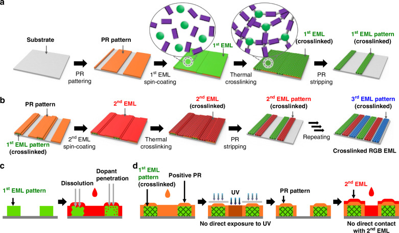 Figure 1
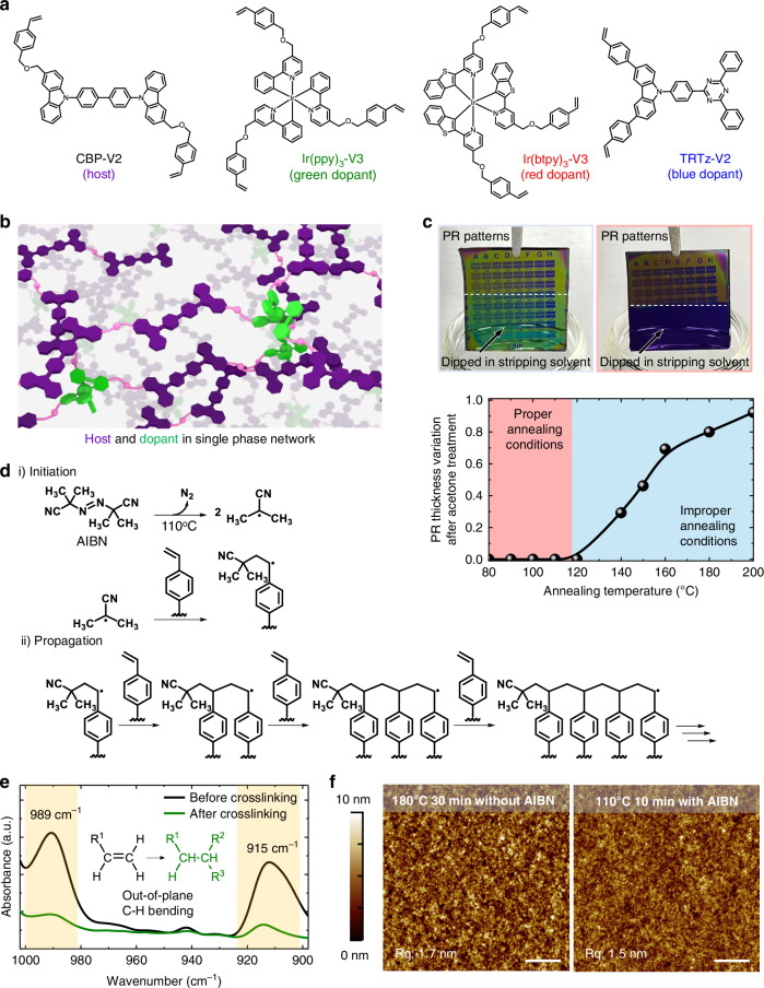 Figure 2
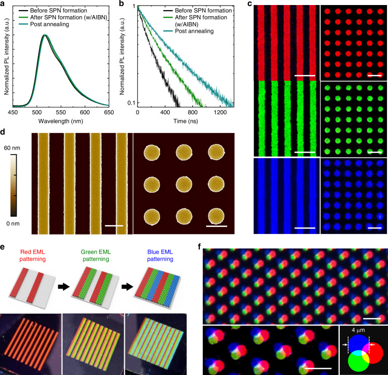 Figure 3
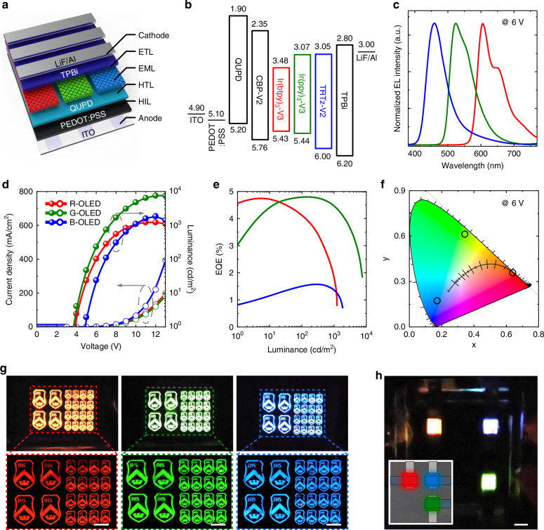 Figure 4
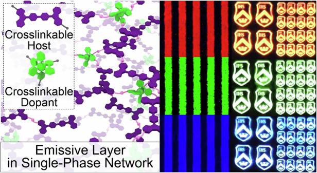 Figure 5
Peer Reviews
No public reviews on file for this paper yet. If you reviewed it on a platform where reviews are public (OpenReview, ICLR, NeurIPS, ICML), you can paste yours below so the community can read it here.
Videos
No videos yet. Explain this paper in a talk, walkthrough, or lecture? Add one.
Taxonomy
TopicsOrganic Light-Emitting Diodes Research · Thin-Film Transistor Technologies · Nanomaterials and Printing Technologies