Atomic Manipulation of 2D Materials by Scanning Tunneling Microscopy: Advances in Graphene and Transition Metal Dichalcogenides
Tingting Wang, Lingtao Zhan, Teng Zhang, Yan Li, Haolong Fan, Xiongbai Cao, Zhenru Zhou, Qinze Yu, Cesare Grazioli, Huixia Yang, Quanzhen Zhang, Yeliang Wang

TL;DR
This paper reviews how scanning tunneling microscopy enables precise atomic-scale manipulation of 2D materials like graphene and TMDs, opening new possibilities in nanotechnology.
Contribution
The paper highlights recent advancements in using STM for atomic manipulation of 2D materials, emphasizing novel techniques and their applications.
Findings
STM allows translational, rotational, and etching operations on 2D materials at the atomic scale.
STM-based manipulation enables stress-induced bandgap modulation and tip-induced phase transformations.
STM offers advantages over traditional methods for constructing nanoscale heterostructures and quantum devices.
Abstract
This review provides a comprehensive overview of recent advances in atomic-scale manipulation of two-dimensional (2D) materials, particularly graphene and transition metal dichalcogenides (TMDs), using scanning tunneling microscopy (STM). STM, originally developed for high-resolution imaging, has evolved into a powerful tool for precise manipulation of 2D materials, enabling translational, rotational, folding, picking, and etching operations at the nanoscale. These manipulation techniques are critical for constructing custom heterostructures, tuning electronic properties, and exploring dynamic behaviors such as superlubricity, strain engineering, phase transitions, and quantum confinement effects. We detail the fundamental mechanisms behind STM-based manipulations and present representative experimental results, including stress-induced bandgap modulation, tip-induced phase…
Genes, proteins, chemicals, diseases, species, mutations and cell lines named across the full text — each resolved to its canonical identifier and authoritative record.
Click any figure to enlarge with its caption.
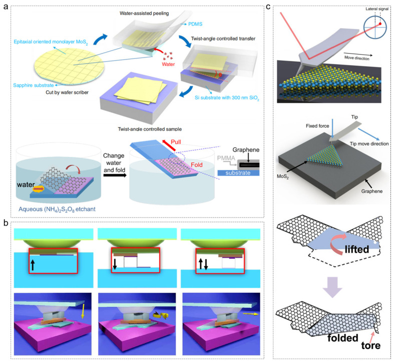 Figure 1
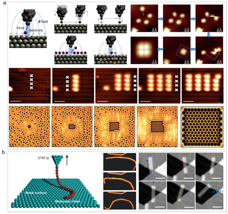 Figure 2
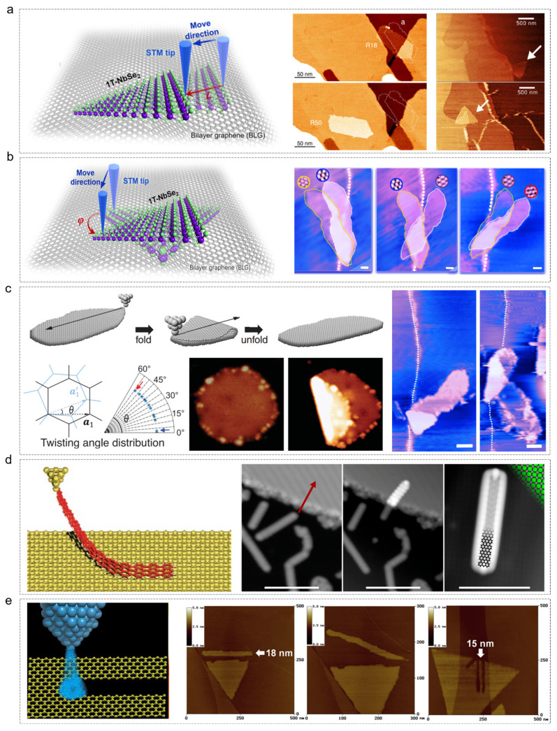 Figure 3
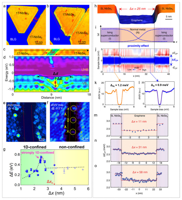 Figure 4
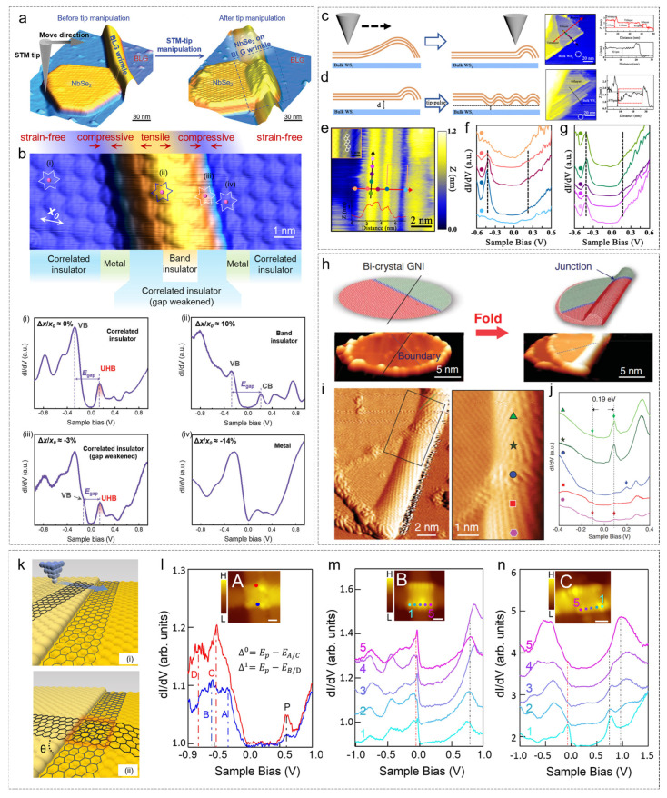 Figure 5
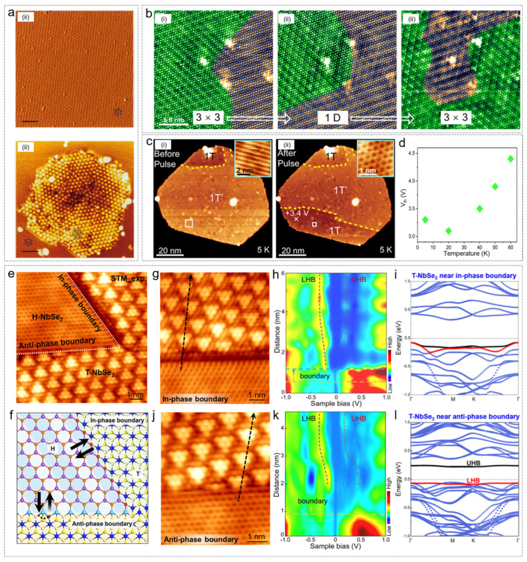 Figure 6
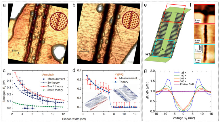 Figure 7
- —the National Key R&D Program of China
- —the National Natural Science Foundation of China
Peer Reviews
No public reviews on file for this paper yet. If you reviewed it on a platform where reviews are public (OpenReview, ICLR, NeurIPS, ICML), you can paste yours below so the community can read it here.
Videos
No videos yet. Explain this paper in a talk, walkthrough, or lecture? Add one.
Taxonomy
Topics2D Materials and Applications · Graphene research and applications · Electronic and Structural Properties of Oxides
1. Introduction
The discovery of graphene in 2004 ignited widespread interest in two-dimensional (2D) materials and their promising applications in next-generation technologies [1]. These materials, composed of monolayers or a few of layers of atomic structures, possess a thickness much smaller than their lateral dimensions [2,3]. Within individual layers, atoms are strongly bonded via covalent interactions, while adjacent layers are held together by weak van der Waals (vdW) forces [4,5]. Due to their unique structural and electronic properties, 2D materials have demonstrated significant potential in electronics [6,7,8,9], optoelectronics [10,11,12,13], and various emerging fields [14,15,16,17,18,19,20,21], positioning them as strong candidates for extending Moore’s Law.
Efficient construction techniques are essential for the reliable characterization and integration of 2D materials into functional devices. The degree of cleanliness achieved during construction directly impacts the stability and reproducibility of their intrinsic properties. Currently, three primary clean construction methodologies are employed—liquid-phase assisted exfoliation [22,23], mechanical transfer [24,25], and scanning probe microscopy (SPM)-based manipulation [14,26,27,28]—along with several other emerging techniques [29]. Liquid-phase assisted exfoliation (Figure 1a) facilitates large-scale material preparation via solution-based processes, but often results in solvent or polymer residues, compromising interfacial purity. Mechanical exfoliation (Figure 1b) enables angular control through prefabricated patches, yet it is constrained by limited material size, precision, and dependency on intermediary layers. In contrast, SPM (Figure 1c) distinguishes itself by operating in dry, ultrahigh-vacuum environments, allowing for direct, contamination-free manipulation of materials at the atomic scale.
SPM offers dual capabilities: high-resolution imaging and precise manipulation of nanoscale materials. Unlike traditional transfer methods, SPM enables the dynamic, controlled positioning of 2D materials, critically influencing properties such as superlubricity [5], superlattice formation [30], and even superconductivity [31]. Its ability to ensure atomic-level cleanliness, combined with exceptional spatial control, makes SPM an ideal platform for the high-precision transfer and performance tuning of 2D materials. In SPM operations, AFM and STM techniques are commonly employed. These two methods are applied in different scenarios. STM utilizes current feedback to acquire sample topography and electronic properties, while AFM primarily relies on force feedback to obtain sample morphology and chemical bonding information. Both techniques can accomplish the structuring of target materials. However, when conducting research on electronic states and conductive properties of two-dimensional materials, the STM manipulation technique demonstrates greater advantages.
This review focuses on five prevalent scanning tunneling microscopy (STM)-based techniques for manipulating 2D materials—primarily graphene and transition metal dichalcogenides (TMDs)—including translation, rotation, folding, picking, and etching. We provide detailed examples of structural modifications achieved through these methods, addressing critical aspects such as interlayer spacing, strain engineering, phase transitions, and the fabrication of custom nanostructures. Finally, we discuss current limitations and outline future directions for the development and application of STM manipulation in advanced material research.
2. STM Manipulation
Scanning probe microscopy (SPM) has revolutionized nanoscience by enabling not only high-resolution imaging but also the precise manipulation of matter at the nanoscale, even down to the individual atoms. SPM uses a sharp tip to probe local surface properties with nanometer or atomic resolution, allowing for the generation of real-space, high-resolution images [32].
Among SPM techniques, STM, developed by Binnig and Rohrer in 1982 [33], has been particularly influential, earning them the Nobel Prize in Physics in 1986. In an STM experiment, a bias voltage is first applied between the sample and the probe. When the distance between the probe and the sample decreases to approximately a few nanometers, a tunneling current caused by the quantum tunneling effect can be detected. Since the tunneling current exhibits an exponentially decaying relationship with the separation between the sample and the tip, the scanning tunneling microscope is highly sensitive to minute topographic variations on the surface. By scanning the tip across the entire sample, the topographic information of the sample surface can be obtained.
2.1. STM Manipulation in Zero-Dimensional and One-Dimensional Materials
The exploration of novel physical properties through dimensional reduction—from three-dimensional (3D) bulk materials to two-dimensional (2D) graphene [34], one-dimensional (1D) carbon nanotubes [35], and zero-dimensional (0D) fullerenes [36] or quantum dots [37] has greatly expanded the frontiers of nanoscience. STM has played a pivotal role in enabling the precise manipulation of 0D molecules (as shown in Figure 2a) [38,39,40,41] and 1D molecular chains (as shown in Figure 2b) [42,43], facilitating atomic-level control.
A landmark achievement was demonstrated by Eigler et al., who arranged Xe atoms on a Ni (110) surface to spell “IBM” with atomic precision [44]. STM has also been used for vertical manipulation, such as transferring CO molecules [45] and Ca dimer clusters [46] between the tip and substrate, and has been employed for on-surface chemical reactions, such as the Ullmann coupling [47]. For 1D systems, STM has been used to construct metal atomic chains [48], spin chains [49], and quantum confinement structures [50]. Moreover, STM allows for the guided alignment of molecular chains, such as CO on Cu (111) to form “molecular graphene” [40], and iodobenzene chains [51]. It further facilitates the fabrication of 1D heterojunctions, such as graphene nanoribbons [52] and semiconductor atomic lines [53].
2.2. STM Manipulation Methods in Two-Dimensional Materials
The STM-based manipulation of 2D materials predominantly involves five distinct techniques: translation [26,54,55,56,57], rotation [26,54,55,56,57], folding [57,58,59,60], picking [61,62,63], and cutting [64,65]. Successful execution of these operations depends critically on achieving ultralow friction between the 2D material and the substrate, a condition associated with superlubricity [16,19,56]. These manipulation strategies enable precise control over both the spatial positioning and geometric configuration of 2D materials.
2.2.1. Translation and Rotation
The ability to translate and rotate 2D materials hinges on minimizing interfacial friction [14,66,67]. When there is significant lattice mismatch between the material and substrate, friction is reduced, facilitating easier manipulation. However, when the lattices are commensurate, as in the case of graphene flakes on graphite [16,68], higher forces are required to overcome the increased friction. The practical examples of translation [54,55,56] and rotation [54,57] are shown in Figure 3a and Figure 3b, respectively. For example, 1T-NbSe_2_ islands grown on bilayer graphene (BLG) can be manipulated via STM tip [54]. The tip is guided along a specific trajectory to the island’s edge, where the repulsive force between the tip and 1T-NbSe_2_ island enables controlled sliding. The STM manipulation protocol requires precise positioning of the scanning probe tip within the quantum tunneling regime (typically maintained at 1 nA tunneling current under −0.1 V bias voltage). The tip is then translated along predefined trajectories with atomic-scale precision, employing a controlled scanning rate below 1 nm/s. During this process, the tip-induced repulsive forces generated in the noncontact tunneling configuration enable controlled displacement of islands by overcoming their interfacial friction with the substrate. Translation distance (L) and rotation angle (φ) can be monitored in real time using atomic-level STM images.
2.2.2. Folding (Origami)
Folding, or nanoscale origami, increases the effective thickness of 2D materials and enables the creation of complex three-dimensional nanostructures as shown in Figure 3c [57,58]. This technique requires the material to be highly flexible—an inherent property of many 2D systems. The process involves initially placing the STM tip on the edge of the 2D materials and gradually reducing the vertical distance between them. This causes an increase in the electrostatic force between the STM tip and the edge. By moving the tip in a specific direction, the edge of the 2D island is lifted and shifted accordingly. The manipulation process involves precisely positioning the STM tip in proximity to the edge of a graphene nanostructure through controlled tip–substrate distance reduction. When the induced van der Waals forces between the tip and nanostructure surpass the interfacial adhesion force binding the nanostructure to the substrate, the tip initiates edge-selective detachment. This enables controlled directional transport of the nanostructure along a predetermined tip trajectory through continuous van der Waals interaction modulation. The process concludes with tip retraction and precise deposition of the relocated nanostructure segment at targeted coordinates, completing the nondestructive nanoscale manipulation cycle. Eventually, the lifted portion is folded onto another part of the graphene, giving rise to graphene-folded nanostructures. Within these intricate nanostructures, the lifted graphene sheet forms a flat stacking structure with the remaining sheets, while a partially closed tubular structure emerges at the connection point. Likewise, if the tip is positioned on the edge of the folded section within the folded graphene nanostructure and the vertical distance between the tip and the edge is gradually reduced, the folded part can be lifted once again by the STM tip and placed back onto the graphite surface. This restores the state of the graphene island prior to folding. This folding and unfolding process of graphene nanoislands can be repeatedly reversed in any direction.
2.2.3. Picking and Transfer
STM can also facilitate the pickup and transfer of nanostructures across steps or onto different substrates, like Figure 3d [61,62]. This method relies on van der Waals or chemical bonding between the tip and the material, forming a suspended junction. The target material to be picked up must be a single crystal or of high crystallinity (e.g., graphene grown by chemical vapor deposition) to avoid defects that could lead to failure or distort transport properties. Typically, the material’s length is less than 50 nm to prevent breakage due to mechanical stress. Narrow-band materials are more likely to form stable suspended junctions. The process begins by confirming the target material’s position and edge structure (e.g., zigzag or armchair type) using atomic resolution STM images. The specific endpoints of the material (such as the zigzag edge) are selected for contact to enhance binding via edge-localized states. The STM tip is then slowly lowered to the material surface, and contact is judged by a current jump (e.g., a sudden decrease from 1 nA to 0.1 nA). Subsequently, the tip is retracted at a constant speed (0.1–1 nm/s), and the current–distance (I–z) curve is monitored. If the current decays exponentially with distance (β ≈ 0.1–0.8 Å^−1^), it indicates that the material has been successfully picked up and a suspended junction has been formed.
2.2.4. Cutting and Etching
STM-based nanofabrication employs tunneling electrons to induce localized etching, enabling precise cutting of graphene and other 2D lattices [65]. The core mechanism involves high-energy tunneling electrons breaking the carbon–carbon bonds (Figure 3e), with the assistance of oxygen or water molecules in the environment, enabling atomic-level edge control. Atomic-resolution images at low bias (5–50 mV) and tunneling currents (1–2 nA) are used to determine the zigzag and armchair crystallographic directions. To induce etching, a negative bias of 2.0–2.3 V is applied to activate the tunneling electron beam. The tip is moved at a speed of 1–5 nm/s along the predefined direction, ensuring continuous cutting. This process is carried out in an atmosphere with humidity levels of 70–75%, where the oxidizing effect of water molecules facilitates the etching reaction.
3. STM Manipulation Application
Atomic-scale manipulation using STM has become indispensable in the study of 2D materials. This technique offers a flexible, contamination-free, and highly precise method for controlling nanoscale structures. As the family of 2D materials continues to grow, research has moved beyond static structural analysis towards the exploration of dynamic, tunable, and multi-dimensional material properties. STM tip-based manipulation provides unique opportunities to investigate and engineer complex behaviors, including electronic coupling, strain effects, phase transitions, and custom nanostructure fabrication.
Apart from altering the electrical properties of materials by positioning the sample, STM techniques can also be utilized to “write” and “read” spin states. [69] Using two STM manipulation approaches—electron-induced dehydrogenation and tip–nanostructure bonding—controllable switching of local spin states in graphene nanostructures has been achieved [70].
3.1. Distance Regulation Between Islands
STM enables the systematic study of electronic phenomena that emerge from varying the spacing between nanoscale islands, such as 1D correlated electronic properties [71,72,73]. By combining atomic-scale imaging with spectroscopic capabilities, STM can precisely characterize both structural morphology and local electronic states as a function of inter-island distance.
Zhang et al. demonstrated that the electronic properties of two 1T-NbSe_2_ islands change dynamically as their separation decreases [54]. When the islands are far apart (Figure 4a), no electronic states are observed in the intervening region, as observed in the corresponding dI/dV map. However, as the islands approach each other, the apparent depth of the homojunction became shallower, and the band bending in the vicinity of the islands also decreased, with the speed of the gap reduction accelerating as the distance between the islands decreased (Figure 4b, with a gap of 2.4 nm). The atomic-resolution image and dI/dV line spectra (Figure 4c,d) showed that the energy bands between the islands bent downward as the spacing reduced.
Moreover, the superconducting properties of single-layer H-NbSe_2_ islands exhibit a significant size dependence, with a critical area of approximately 800 nm^2^ [74]. When the island area (S) exceeds this critical value, scanning tunneling spectroscopy (STS) reveals particle–hole symmetric coherence peaks, indicating the presence of a uniformly distributed superconducting gap (approximately 1.2 meV), with the gap extending to the island’s edge. However, when S < 800 nm^2^, the superconductivity is suppressed and transitions to insulating behavior, likely due to Coulomb gaps induced by quantum confinement effects.
When such superconducting islands form an Ising superconductor–normal metal-Ising superconductor (INI) Josephson junction with graphene, a spatially uniform superconducting gap (approximately 0.9 meV) can be induced in graphene. Experiments confirm that even when the distance (Δx) between NbSe_2_ islands is artificially expanded to 150 nm, graphene still maintains a superconducting gap, with only a slight decay at the center, which contrasts sharply with the much smaller decay length observed in conventional NbSe_2_–metal junctions. This is likely due to the enhanced proximity effect from multiple Andreev reflections at both interfaces. This macroscopic superconducting phenomenon induced by a high-density array of NbSe_2_ islands provides a new avenue for the design of graphene-based quantum devices.
3.2. Strain Regulation
Mechanical strain offers a powerful lever to modulate the physical, chemical, and electronic properties of 2D materials, enabling the design of tunable functional devices. STM manipulation provides nanoscale control over strain application.
Hou et al. manipulated the T-phase NbSe_2_ islands grown on BLG using STM tip control, moving the islands from the wrinkle side to the wrinkle itself (Figure 5a) [75]. It was observed that the NbSe_2_ islands at different positions on the wrinkle experienced varying degrees of tensile and compressive stress. This stress caused changes in the bandgap of the insulating NbSe_2_ phase. In region (ii) of Figure 5b under tensile stress, the NbSe_2_ bandgap broadened, transforming from a Mott insulator to a band insulator. In region (iii) of Figure 5b, under compressive stress, the bandgap was compressed, and as the compression increased, the gap gradually decreased until it became metallic, as shown in region (iv) of Figure 5b.
Guan et al. transferred few-layer graphene onto bulk WS_2_ substrates and used STM tip manipulation to control the graphene wrinkles, investigating the effect of stress on the graphene bandgap [76]. The manipulation methods are shown in Figure 5c,d. In Figure 5c, the STM image shows the morphology after the wrinkles were smoothed by the STM tip. The height profile on the right indicates that the graphene was flattened, with only one remaining wrinkle. The tip pulse method was then used to reconstruct graphene nanowrinkles, reducing the distance between the wrinkle valley and the substrate, enhancing the coupling between graphene and WS_2_, and opening the graphene bandgap. A metal–semiconductor–metal structure was constructed on the graphene nanosheet.
From the above experiments, it is evident that stress engineering provides an efficient way to open the graphene bandgap. In 2019, Chen et al. used STM tip manipulation to fold graphene on a HOPG substrate [58]. This folding was repeatable and could be carried out at arbitrary angles. By selecting the folding direction, they could customize the semiconductor or metallic tube-like edges. In addition to folding graphene sheets, they also folded bicrystalline graphene nanodisks with 5–7 ring grain boundaries. After folding, the defects in the original plane evolved into molecular heterojunctions (IMJs) connecting two different chiral carbon nanotubes (CNTs). The van Hove singularity (VHS) bandgap of both segments of the tubes was 0.19 eV, indicating that their semiconducting properties were mainly determined by the tube diameter.
Further, in 2020, Chen et al. successfully controlled the twist angle of bilayer graphene using the STM tip manipulation method with a configuration of a periodic alternation of pentagons and heptagons grain boundary [77]. Later, in 2022, they used the STM tip to construct bilayer zigzag graphene nanoribbons (6-GNR) with a specific twist angle (θ) on a Au (111) surface [78]. Experimental and theoretical studies revealed that two stacked 6-GNRs with the same twist angle (θ = 90°) exhibited three different stacking offsets in the twisted bilayer zigzag GNR junction: Model A (high-symmetry stacking), Model B (low-symmetry stacking), and Model C (asymmetric stacking). The edge states of these three stacking configurations were significantly different. In Model A, the STS spectrum showed a clear bandgap at the edges, which was significantly smaller than the bandgap of a single-layer zigzag GNR (Δ^0^ = 1.5 eV). No near-zero energy peak was observed, indicating that flat bands did not form under high-symmetry stacking. In Model B, the near-zero energy peak expanded, corresponding to the formation of flat bands, and the bandgap further reduced, indicating stronger interlayer coupling. In Model C, a near-zero energy peak was observed only at the junction corner (point I), rapidly decaying towards the opposite corner (point S), as shown by the red dashed line.
3.3. Phase Transformation Induced by STM
STM tip-induced voltage pulses can drive local phase transitions in 2D materials, offering a direct method to engineer electronic phases with spatial precision.
In 1996, Zhang et al. first demonstrated STM-induced phase transition in TaSe_2_ [79]. In 2017, Bischof et al. later triggered a local phase transition of NbSe_2_ from the 2H phase to the 1T phase by applying voltage pulses greater than 4 V (lasting 100 ms) [80]. Additionally, using low-temperature STM, they performed reversible phase transitions on the surface of NbSe_2_ at high-bias voltages (5–6 V). When the STM tip repeatedly scanned with a 5–6 V high bias, part of the 3 × 3 charge density wave (CDW) region transformed into a 1D CDW. After lowering the bias and scanning again, the 1D CDW region reverted to the original 3 × 3 CDW structure, demonstrating the reversibility of the phase transition. The high-bias voltage from the STM tip may induce lattice strain via localized Joule heating or charge injection, breaking the symmetry of the 3 × 3 CDW and promoting its transformation into a strain-stabilized 1D-CDW. In addition to modulating the period of the CDW in the sample, Song et al. also successfully manipulated the hand phase of the CDW in T-phase NbSe_2_ via tip-induced pulses [81].
In a 2024 study, the authors explored the voltage pulse-induced 1T’→1T structural phase transition in monolayer FeSe_2_ at various temperatures [82]. They investigated the threshold voltage and reversibility of the phase transition at temperatures ranging from 5 K to 60 K. The study found that as the temperature increased, the threshold voltage for the phase transition increased. Above 50 K, the 1T phase spontaneously reverted to the 1T’ phase. At 60 K, 54% of the islands could not be converted by the pulse. Ren et al. utilized STM voltage pulses to induce local mechanical fractures and phase transitions at the interface of graphene–WSe_2_ heterostructures, achieving the transformation of WSe_2_ from the 1H phase to the 1T’ phase [83].
In a more detailed study by Chen et al. in 2025, the researchers observed two types of boundaries after applying voltage pulses based on whether the selenium atoms were aligned in the same direction [84]. Boundaries with selenium atoms aligned along the same line were termed “same-direction”, while those with misaligned atoms were referred to as “opposite-direction”. High-resolution morphology images in Figure 6g,j show these two types of boundaries. The line spectra in Figure 6h,k reveal that at the same-direction boundary, the material exhibits metallic behavior in the H phase, whereas at the opposite-direction boundary, the material retains the insulating behavior of the T phase. Density functional theory (DFT) calculations of the band structure show that at the same-direction boundary, the UHB (upper Hubbard band) is absent in T-NbSe_2_, while at the opposite-direction boundary, the UHB shifts upward, and the bandgap between the UHB and LHB (lower Hubbard band) widens.
3.4. Atomic-Scale Etching and Nanostructure Customization
STM-based nano-etching has evolved through several key stages. In the 1980s, STM demonstrated nanoscale processing capabilities, enabling the etching of nanowires and conical structures on metal surfaces [85,86,87]. By the 1990s, electrochemical oxidation etching emerged as a breakthrough, with STM inducing local oxidation on hydrogen-passivated silicon, achieving precise nanostructure etching [88]. Simultaneously, thermal decomposition and electron beam etching advanced STM’s application under high-temperature and electron energy control [89]. As the technology progressed, STM expanded into electrochemical etching in liquid environments, enabling atomic-scale precision in more complex materials. By the late 1990s, STM achieved ultimate resolution with single-atom manipulation at ultralow temperatures, demonstrating atomic-level precision.
In 2014, researchers utilized STM-based etching techniques to create GNRs with precisely defined edge configurations and widths [65]. As shown in Figure 7a, the study investigated the effects of armchair and zigzag edge structures, as well as different widths, on the electrical conductivity and magnetism of graphene nanoribbons. Through a combination of theoretical and experimental work, it was found that when the width of the graphene nanoribbon was less than 7 nm, zigzag-edge ribbons exhibited a 200–300 meV bandgap, which arises from electron–electron interactions. However, when the width exceeded 8 nm, the bandgap disappeared. In contrast, the bandgap of armchair-edge nanoribbons (E_g_) was inversely proportional to their width (W).
In addition, using STM lithography, the researchers etched nanoscopic constrictions (GNCs) in graphene nanoribbons with atomic precision, achieving sizes on the order of a few nanometers [90]. The high bias and strong tunneling current from the STM locally broke carbon–carbon bonds, forming the constrictions while maintaining the integrity of the surrounding graphene. Following the introduction of the constriction, the current–voltage (I–V) curve became nonlinear, with a transport gap (Δ ≈ 10 meV) emerging at low-bias voltages. The height of the conductance peak exhibited an exponential decay with increasing temperature but remained clearly visible even at room temperature (300 K).
4. Summary and Perspectives
Combined with its exceptional precision for atomic-scale synthesis and manipulation, STM establishes a versatile platform for quantum research and the rational design of advanced materials—from molecular graphene to fractal nanostructures. Compared to alternative transfer methods, SPM-based techniques (particularly STM) enable nondestructive nanoscale manipulation with customizable geometry control while maintaining single-atom precision. Unlike AFM, which relies on tip–surface contact interactions, STM’s quantum tunneling-based noncontact operation not only permits atomic-resolution material restructuring but simultaneously provides real-time electronic characterization through current–voltage spectroscopy. This dual capability to both engineer matter at the fundamental quantum level and probe emergent physical phenomena enables: (1) the systematic construction of tailored nanoscale architectures with programmed electronic properties, and (2) the fundamental exploration of low-dimensional quantum systems through atom-by-atom fabrication. Certainly, the application of STM manipulation technology still faces significant challenges. Despite its strengths, several critical barriers persist. Currently, STM techniques are limited to small-sized samples and demand exceptionally high cleanliness standards for both specimens and the scanning environment. Furthermore, the process is vulnerable to interference from environmental vibrations, thermal drift, and electronic noise, undermining environmental stability during operations. While manual STM manipulation allows for precise atomic-level control, its low efficiency hampers the automation required for fabricating complex nanostructures and achieving large-scale assembly. Scaling these laboratory-proven techniques to practical industrial device fabrication introduces additional technical hurdles, particularly in maintaining precision and reproducibility at macroscopic scales. Addressing these limitations—automation capabilities, environmental robustness, and scalable manufacturing—remains pivotal for transitioning STM from a research tool to a mainstream nanofabrication platform.
This review has summarized the principal methods and recent advances in STM-based manipulation of two-dimensional materials, emphasizing its role in enabling precise structural control and property tuning. Looking ahead, the integration of STM with artificial intelligence (AI) holds great potential to transform nanofabrication. AI-driven approaches could facilitate autonomous manipulation, optimize experimental parameters in real time, and accelerate the design of functional nanodevices. As these interdisciplinary technologies evolve, STM is expected to play an increasingly pivotal role in the future of electronics, photonics, biomedicine, and nanoscale systems engineering.
The reference list from the paper itself. Each links out to its DOI / PubMed record.
- 1Novoselov K.S. Geim A.K. Morozov S.V. Jiang D. Zhang Y. Dubonos S.V. Grigorieva I.V. Firsov A.A. Electric field effect in atomically thin carbon films Science 200430666666910.1126/science.110289615499015 · doi ↗ · pubmed ↗
- 2Tan C. Cao X. Wu X.-J. He Q. Yang J. Zhang X. Chen J. Zhao W. Han S. Nam G.-H. Recent Advances in Ultrathin Two-Dimensional Nanomaterials Chem. Rev.2017117622563312830624410.1021/acs.chemrev.6b 00558 · doi ↗ · pubmed ↗
- 3Zhang H. Ultrathin Two-Dimensional Nanomaterials ACS Nano 201599451946910.1021/acsnano.5b 0504026407037 · doi ↗ · pubmed ↗
- 4Lin C.-Y. Wu J.-Y. Chiu Y.-H. Chang C.-P. Lin M.-F. Stacking-dependent magnetoelectronic properties in multilayer graphene Phys. Rev. B 20149020543410.1103/Phys Rev B.90.205434 · doi ↗
- 5Shinjo K. Hirano M. Dynamics of friction: Superlubric state Surf. Sci.199328347347810.1016/0039-6028(93)91022-H · doi ↗
- 6Cao Y. Fatemi V. Fang S. Watanabe K. Taniguchi T. Kaxiras E. Jarillo-Herrero P. Unconventional superconductivity in magic-angle graphene superlattices Nature 2018556435010.1038/nature 2616029512651 · doi ↗ · pubmed ↗
- 7Zhao C. Tan C. Lien D.-H. Song X. Amani M. Hettick M. Nyein H.Y.Y. Yuan Z. Li L. Scott M.C. Evaporated tellurium thin films for p-type field-effect transistors and circuits Nat. Nanotechnol.202015535810.1038/s 41565-019-0585-931844286 · doi ↗ · pubmed ↗
- 8Koman V.B. Liu P. Kozawa D. Liu A.T. Cottrill A.L. Son Y. Lebron J.A. Strano M.S. Colloidal nanoelectronic state machines based on 2D materials for aerosolizable electronics Nat. Nanotechnol.20181381982710.1038/s 41565-018-0194-z 30038369 · doi ↗ · pubmed ↗