Correction: A Valuable and Low-Budget Process Scheme of Equivalized 1 nm Technology Node Based on 2D Materials
Yang Shen, Zhejia Zhang, Zhujun Yao, Mengge Jin, Jintian Gao, Yuhan Zhao, Wenzhong Bao, Yabin Sun, He Tian

Abstract
Genes, proteins, chemicals, diseases, species, mutations and cell lines named across the full text — each resolved to its canonical identifier and authoritative record.
Click any figure to enlarge with its caption.
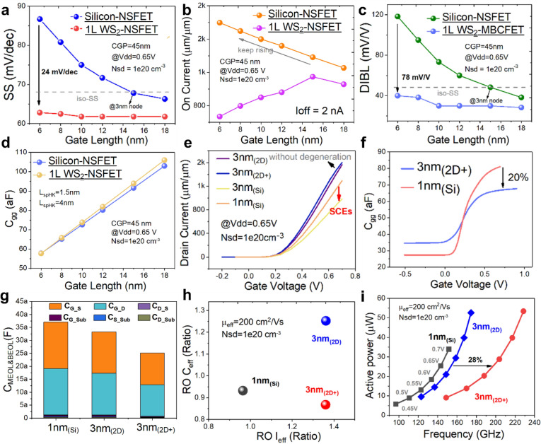 Figure 1
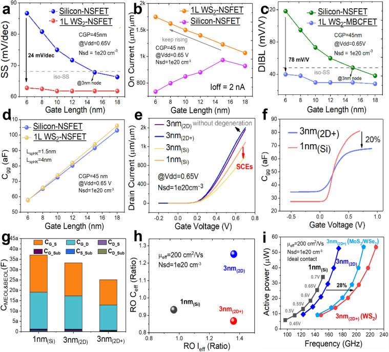 Figure 2
Peer Reviews
No public reviews on file for this paper yet. If you reviewed it on a platform where reviews are public (OpenReview, ICLR, NeurIPS, ICML), you can paste yours below so the community can read it here.
Videos
No videos yet. Explain this paper in a talk, walkthrough, or lecture? Add one.
Taxonomy
TopicsFerroelectric and Negative Capacitance Devices
Correction to: Nano-Micro Letters (2025) 17:191 10.1007/s40820-025-01702-7
Following the publication of the original article [1], the authors reported an error in Fig. 3(b), and the figure legend was reversed.
The correct Fig. 3 has been provided in this orrection.
The incorrect Fig. 3 is:Fig. 3. Comparison of electrical characteristics of devices at 3 nm_(2D+)_ node, 3 nm_(2D)_ node and 1 nm_(Si)_ node, with fixed CGP of 45 nm and LG shrinking from 18 to 6 nm for Si-NSFETs and WS_2_ NSFETs. a SS variation, the SS of Si-NSFETs degrades drastically when the L_G_ is smaller than 12 nm, and b ION variation, thanks to the smaller feature length of 2D materials, the ION of WS_2_ NSFETs continues to increase even with the LG scaled to 6 nm, while the I_ON_ of Si-NSFETs degrades continuously when the LG is reduced to 6 nm; c DIBL variation, which follows a similar trend to that of SS; d C_gg_ variations, with EOT and gate size being the main influences on Cgg; e Linear transfer characteristics corresponding to four devices, at 3 nm_(2D), 3 nm(2D+), 3 nm(Si)_ and 1 nm_(Si); f Cgg-VGS relationship for 3 nm(2D+)_ and 1 nm_(Si)_ counterparts, which is reduced by 20% for the 3 nm_(2D+)_ due to shortened LG; g C_MEOL&BEOL_ comparison with middle end of line (MEOL) and back end of line (BEOL) parasitic capacitances; h Comparison of equivalent capacitances and equivalent currents extracted from RO circuits; and i Power–frequency comparison of RO circuits
The correct Fig. 3 is:Fig. 3. Comparison of electrical characteristics of devices at 3 nm_(2D+)_ node, 3 nm_(2D)_ node and 1 nm_(Si)_ node, with fixed CGP of 45 nm and LG shrinking from 18 to 6 nm for Si-NSFETs and WS_2_ NSFETs. a SS variation, the SS of Si-NSFETs degrades drastically when the L_G_ is smaller than 12 nm, and b ION variation, thanks to the smaller feature length of 2D materials, the ION of WS_2_ NSFETs continues to increase even with the LG scaled to 6 nm, while the I_ON_ of Si-NSFETs degrades continuously when the LG is reduced to 6 nm; c DIBL variation, which follows a similar trend to that of SS; d C_gg_ variations, with EOT and gate size being the main influences on Cgg; e Linear transfer characteristics corresponding to four devices, at 3 nm_(2D), 3 nm(2D+), 3 nm(Si)_ and 1 nm_(Si); f Cgg-VGS relationship for 3 nm(2D+)_ and 1 nm_(Si)_ counterparts, which is reduced by 20% for the 3 nm_(2D+)_ due to shortened LG; g C_MEOL&BEOL_ comparison with middle end of line (MEOL) and back end of line (BEOL) parasitic capacitances; h Comparison of equivalent capacitances and equivalent currents extracted from RO circuits; and i Power–frequency comparison of RO circuits
The original article [1] has been corrected.