Landauer Resistivity Dipole at One-Dimensional Defect Revealed via near-Field Photocurrent Nanoscopy
Francesca Falorsi, Marco Dembecki, Christian Eckel, Monica Kolek Martinez de Azagra, Kenji Watanabe, Takashi Taniguchi, Martin Statz, R. Thomas Weitz

TL;DR
Researchers used a high-resolution imaging technique to observe how electrical resistance behaves at a tiny graphene interface, confirming a long-standing theoretical model.
Contribution
The study experimentally demonstrates Landauer resistivity dipoles at a one-dimensional graphene interface using near-field photocurrent imaging.
Findings
Charge carrier accumulation was observed around the graphene interface due to Landauer resistivity dipoles.
Photocurrent polarity matched the applied voltage at low doping levels but disappeared at higher densities.
The results align with numerical calculations and validate the use of photocurrent nanoscopy for studying nanoscale resistance.
Abstract
The fundamental question of how to describe ohmic resistance at the nanoscale was answered by Landauer in his seminal picture of the Landauer resistivity dipole (LRD). While this picture is theoretically well understood, experimental studies remain scarce due to the need for noninvasive local probes. Here, we use the nanometer lateral resolution of near-field photocurrent imaging to thoroughly characterize a monolayer–bilayer graphene interface. Via systematic tuning of charge carrier density and current flow, we detected charge carrier accumulation around this nearly ideal one-dimensional defect due to the formation of the LRDs. We found that, at low doping levels, the photocurrent exhibits the same polarity as the applied source–drain voltage, reflecting carrier concentration changes induced by the LRDs. This signature disappears at higher charge carrier densities in agreement with…
Genes, proteins, chemicals, diseases, species, mutations and cell lines named across the full text — each resolved to its canonical identifier and authoritative record.
Click any figure to enlarge with its caption.
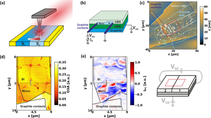 Figure 1
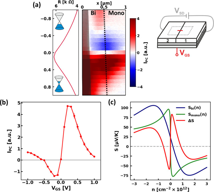 Figure 2
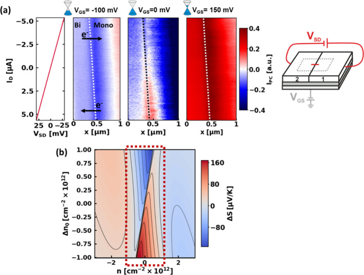 Figure 3
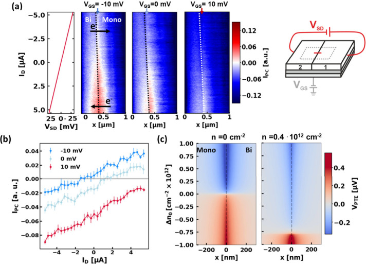 Figure 4
 Figure 5
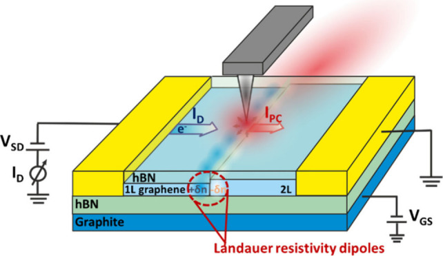 Figure 6
 Figure 7
 Figure 8
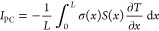 Figure 9
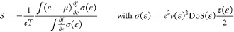 Figure 10
 Figure 11
 Figure 12
 Figure 13
- —Deutsche Forschungsgemeinschaft10.13039/501100001659
- —Deutsche Forschungsgemeinschaft10.13039/501100001659
- —Deutsche Forschungsgemeinschaft10.13039/501100001659
- —Japan Society for the Promotion of Science10.13039/501100001691
- —Japan Society for the Promotion of Science10.13039/501100001691
- —Ministry of Education, Culture, Sports, Science and Technology10.13039/501100001700
- —Core Research for Evolutional Science and Technology10.13039/501100003382
- —Center for NanoScience, Ludwig-Maximilians-Universit?t M?nchen10.13039/501100007153
- —NIM Nanosystems Initiative MunichNA
Peer Reviews
No public reviews on file for this paper yet. If you reviewed it on a platform where reviews are public (OpenReview, ICLR, NeurIPS, ICML), you can paste yours below so the community can read it here.
Videos
No videos yet. Explain this paper in a talk, walkthrough, or lecture? Add one.
Taxonomy
TopicsGraphene research and applications · Nanowire Synthesis and Applications · Semiconductor materials and interfaces
As the scaling of electrical integrated circuits down to a few nanometer sizes continues, the associated increase in current densities intensifies detrimental effects such as electromigration and excess heat generation.? Consequently, understanding the precise mechanisms that govern electronic flow and resistivity on a nanoscopic level is a topic that continues to attract experimental and theoretical research. ?−? ? ? One fundamental mechanism of resistance at the nanoscale, proposed by Landauer, involves the creation of residual resistivity dipoles, often referred to as Landauer resistivity dipoles (LRDs). ?−? ? ? According to the LRD theory, localized dipoles form around defects during current flow, serving as a nanoscopic cause of resistance. Consequently, the voltage drop throughout the material is not homogeneous but rather highly concentrated around these defects.
To add further understanding to this picture, it would be helpful to directly observe these dipoles. The spatial long-range dipolar electric field generated by the LRD is challenging to access experimentally in three dimensions, due to its inherently low dipole strength.? It was recognized early on? that, in two dimensions, the spatial extent of the LRD is larger than in 3D, due to decreased screening.? In general, the local potential build-up by the LRD in 2D is given by
where p is the dipole moment and θ is the angle between r (the distance from the scatterer) and the current.? In the diffusive limit, the total electric field caused by the dipoles surrounding the scatterer, defined as E ^dip^ = n s p, is equal to the Ohmic electric field across the sample. Consequently, the LRD dipole strength is given by
where σ is the conductivity of the sample, j the incident current density, and n s the density of scatterers.? The potential buildup due to the LRD increases with current density and higher sample resistivity. Especially interesting are, therefore, 2D systems, such as van der Waals materials, ?−? ? ? in which both σ and j can be tuned in situ, making them an ideal system to study the LRD. Graphene, ?−? ? in particular, serves as an excellent platform to investigate the effects of scatterers on a local scale. Scatterers not only influence the local buildup of LRD but also affect the local dissipation,? which can be elegantly imaged by scanning SQUID. ?,? However, the LRDs do not contribute relevantly to Joule heating, thus different imaging techniques are required. One approach involves scanning tunneling potentiometry (STP) and conductive AFM, which have been employed to study the LRD formation in 2D materials.
Indeed, the localized voltage drop across scatterers in graphene and monolayer (ML)/bilayer (BL) graphene interface junctions was experimentally measured on devices grown on silicon carbide using STP at low temperatures (ranging from 6 K to 80 K) ?,?−? ? ? and conductive AFM.? In these studies, the Fermi energy is maintained constant. Ji et al.? and Willke et al.? showed that the localized voltage drop has a sign and magnitude related to the current flow. Similar measurements were done on p–n junctions of graphene on h-BN? and on graphene with localized charged defects.? While these fundamental studies show part of the expected response of the LRD at cryogenic temperatures, signatures of LRD under technologically relevant conditions (room temperature) or as a function of current under control of the Fermi energy (and with it, the conductivity), to the best of our knowledge, have not been performed.
Here, we discuss systematic investigations of a graphene ML to a Bernal-stacked BL interface as a function of electrostatically tuned charge carrier density (which controls σ) and current density j to locally identify the LRD. The wave function mismatch at this interface reduces electron transmission, allowing us to consider it as a reflective wall.? To study the local buildup of carriers at the ML/BL interface as a function of σ and j, we use photocurrent imaging, which was successfully used to study lateral charge accumulation in van der Waals materials such as graphene.? Governed by the photothermoelectric effect in graphene, this method is particularly sensitive to the local Seebeck coefficient and thus chemical potential. ?−? ? To allow for a nanoscale resolution, we use scanning near-field optical microscopy (SNOM) ?−? ? which enables photocurrent mapping at a scale equivalent to the tip radius (∼20 nm). ?,? High-resolution SNOM photocurrent nanoscopy in graphene systems has been used for the detection of propagating collective carrier modes, ?,? domain walls, ?−? ? and electronic transport phases in twisted graphene samples at low temperatures. ?,?
We exploit the sensitivity of the photocurrent measured with SNOM to the local chemical potential gradient and use it to study the formation of LRD at ML/BL graphene interfaces during current flow under ambient conditions. We complement our experimental results with numerical calculations, which confirm that the formation of LRDs at the interface leads to a change in polarity of the photocurrent response upon changing the applied bias when the device is near its charge neutrality point (CNP), i.e., at low doping levels. This signature disappears at higher doping concentrations, where the device response is dominated by carrier type, with minimal influence from the LRDs. With our measurements, we are thus able to consistently map the density and current dependence of the LRD in real space.
We first explain the general mechanism by which a photocurrent (I PC) in graphene can emerge, before introducing our measurements. When electrons in graphene are excited by incident radiation, the absorbed photon energy is rapidly transformed into the formation of a hot Fermi distribution by electron–electron scattering. Due to the low electron–phonon coupling, electron cooling is inefficient, allowing hot electrons to remain decoupled from the lattice for relatively long times (from picoseconds up to milliseconds). ?,?,?,? The hot electrons can then produce a net photocurrent at local regions characterized by inhomogeneous profiles of the thermopower (i.e., Seebeck coefficient). In our specific case of the ML/BL interface, when we consider x to be the direction perpendicular to the interface, I PC can be expressed as?
where σ(x) is the spatially dependent conductivity, T(x) is the elevated electron temperature profile induced by the SNOM tip, S(x) is the spatially dependent Seebeck coefficient, and L is the distance between the source and drain contacts. In our case, if we consider the only source for a spatially varying Seebeck coefficient to be the ML/BL interface, the Seebeck coefficient can be modeled as a step function, and the photocurrent signal depends on the Seebeck coefficient difference across the interface (ΔS = S BL – S ML).?
In the semiclassical Boltzmann formalism under the relaxation time approximation, the Seebeck coefficient (S) can be written as?
where e is the electron charge, T the temperature, f the Fermi distribution, σ(ε) is the energy-dependent conductivity, and μ the chemical potential. The electrical conductivity σ depends on the electron velocity (v), the density of states (DoS), and the scattering time (τ). ?,? The chemical potential (μ) is a direct function of the local carrier density n, since, near the CNP, it holds that μ^mono^ = ? and μ^bi^ = ,? where ℏ is the reduced Planck’s constant, v F is the Fermi velocity, and m is the effective mass of the electrons in bilayer graphene, which is defined as m ≅ 0.033 m e, with m e being the electron mass.? Consequently, the scanning photocurrent measurements, directly related to the local Seebeck coefficient, act as a sensitive probe for the local carrier density and, thus, the occurrence of the LRD.
The photocurrent measurements are performed using an SNOM with an illumination wavelength of λ = 10.551 μm. Integrated electrical measurement units enable photocurrent measurements parallel to the optical ones, and in-situ control of the source-drain (V SD) and back-gate (V GS) voltages applied to the system (Figurea). The locally detected photocurrent signal is demodulated with the first or second harmonic of the tip oscillation frequency (Ω), which allows the suppression of the far-field background signal.
To analyze the carrier accumulation of impinging electrons at the ML/BL interface, the two main contacts for the source and drain are placed parallel to the interface. With this geometry, it is possible to probe the Seebeck coefficient gradient perpendicular to the current flow induced by the LRD. ?,? In both samples analyzed for this study, the graphene interface is encapsulated between two hexagonal boron nitride (hBN) flakes, the upper one being thinner than 7 nm, to retrieve the photocurrent signal originating from the underlying graphene.? Graphite gates are used to improve signal quality and reduce energetic disorder in the active layers. The optical images of the used flakes are shown in Figure S2. A schematic of the investigated device structure is shown in Figureb, while AFM topography scans of the two samples considered for this study are shown in Figuresc and Figure S3, where one can notice the cracks and bubbles created during the sample fabrication. Since the samples show similar results, the discussion below focuses on the sample shown in Figurec, while the complementary results of the second sample are shown in the Supporting Information.
Figuresd and ?e show a spatial scan of the area highlighted by the dotted red rectangle in Figurec performed with the SNOM, Figured shows the third harmonic optical amplitude image, while Figuree shows the second harmonic photocurrent signal that is recorded simultaneously. The schematic next to Figuree highlights the fact that, in the acquisition of this photocurrent signal, none of the other parameters that could be varied during the measurement, such as the V GS or V SD, are adjusted; instead, the contacts are left floating. This scheme is maintained throughout the manuscript, with the main varying parameter of each respective photocurrent scan highlighted in red.
The photocurrent scan in Figuree shows that the main signal is generated by the spatial inhomogeneities of the sample, such as cracks or bubbles that are created during fabrication. In these regions, the carrier density and strain of the sample vary, resulting in a spatial texture of the Seebeck coefficient across the sample. ?,? In the rest of the work, we will focus on the photocurrent traces recorded perpendicular to the ML/BL interface, indicated by the faint gray line in Figured. We use the interface as a well-localized one-dimensional (1D) defect for the investigation of the LRD. To establish the photocurrent measurements, we map (Figurea) the photocurrent as a function of charge carrier density, which is electrostatically controlled by the graphite gate (V GS). An additional small constant V SD (1 mV) is applied to monitor the system resistance, which is shown for each point of the scan in the curve to the left of the scan. The dotted line indicates the position of the ML/BL interface. This position is obtained by aligning the photocurrent map with the third harmonic optical amplitude images, where the ML/BL interface is discernible by a difference in optical contrast, as shown, for example, in Figures S6 and S7. This alignment method is used throughout the manuscript.
As the gate voltage is tuned from negative to positive values, the induced carrier density transitions from holes to electrons, as shown in the schematic representation in Figurea. In this density region, the photocurrent near the interface exhibits a double sign switch, as highlighted by the line cut in Figureb, which is taken directly at the ML/BL interface. This behavior is related to the thermoelectric origin of the photocurrent, which depends on the difference in Seebeck coefficients between the ML and the BL graphene, ΔS.? To understand the signal in more detail, we have numerically calculated the Seebeck coefficient of the ML, the BL, and the respective ΔS in Figurec. The Seebeck coefficient is simulated based on eq, without considering the density dependence of τ; ?,?,? more details are provided in S1. The simulated ΔS (Figurec) shows, as expected, the photocurrent’s density dependence with a double sign switch. The reason for this double sign switch is that the difference in band structure between ML and BL leads to a smoother transition of the Seebeck coefficient of the BL from electron- to hole-dominated transport, compared to the ML. ?,? The consistency of electrical measurements and simulations confirms the good understanding of the system.
The photocurrent signal has also a characteristic extent in the direction perpendicular to the interface. In Figurea, one can see that, after a maximum value around the CNP, the photocurrent in the ML decreases, and finally disappears for V GS > 0.9 V on the electron and <-0.5 V on the hole side. In contrast, the photocurrent in the BL remains significant in the entire gate voltage window. The different spatial dependence of I PC in the ML vs the BL arises because the I PC is influenced not only by ΔS but also by the spatial extent of the temperature profile induced by the SNOM illumination (see eq). This profile is determined by the “cooling length”. ?,? The cooling length of the hot electrons (L cool) is defined as L cool = , where κ is the thermal conductivity and g is a constant that accounts for the dispersion of the heat into the substrate.? According to the Wiedemann–Franz law, κ is proportional to the conductivity of the sample.? The lower resistance of the BL results in a longer L cool than the ML (as shown in the measurements in Figure S5).
After having characterized the ML/BL in detail, we turn to the investigation of the LRD. The LRD potential at the interface translates into a local carrier buildup and, consequently, to a ΔS change, which we can locally measure as I PC. To investigate the local carrier accumulation at the interface due to the LRDs, the photocurrent response of the ML/BL interface is studied with respect to the applied bias. To this end, a line scan along the same position as in Figurea is performed with varying I D at a fixed V GS. Figurea shows these scans for three constant V GS values: in the hole-doped regime (V GS = −100 mV), at the local CNP (V GS = 0 V), and in the electron-doped regime (V GS = 150 mV). We examine specifically the low-bias regime (|V SD| < 30 mV), where I PC is generated by the PTE and is not expected to depend on I D. This is seen for scans taken in the doped regimes at V GS = −100 mV and V GS = 150 mV (Figurea). We note in passing that we can consequently also rule out that I PC is due to the bolometric effect, where I PC should indeed depend on the magnitude and sign of the applied bias ?−? ? (see Figure S7 for more details).
In contrast to these scans at high carrier density, a strong I PC dependence on I D is visible for the scan taken around the CNP (Figurea). We attribute this to the local formation of LRDsdue to the applied I _D_which leads to a density difference Δn 0 across the interface and, with it, a ΔS, which we detect as localized I PC. This hypothesis is confirmed by numerical calculations (Figureb) of ΔS at the ML/BL junction, as a function of Δn 0 (caused by LRD V(r) ≈ I D) and n (controlled by V BG). In our calculations, we add, for each data point, Δn 0/2 carriers to the ML and −Δn 0/2 to the BL. Most interesting is the region within the dashed box (Figureb) near the CNP, where a sign change of I D also leads to a sign change of ΔS, which should thus appear in I PC. This is expected, because near the CNP, a small Δn 0 is sufficient to induce electron transport on one side of the interface and hole transport on the other, leading to large differences in the Seebeck coefficients of the two regions (see Figurec). At higher n, the overall impact of the LRD induced Δn 0 on ΔS is comparatively small.
We have also analyzed the detailed I PC (vs I D) dependence in a small V GS window around the CNP in Figure. There, one can discern that I PC is characterized by two main features: it is symmetric around the interface, with an intensity decreasing with the increasing distance from the interface, and it increases with higher I D. Furthermore, the I D position for which the I PC switches sign increases for V GS further from the local CNP (around V GS = −10 mV). This trend is highlighted by vertical line cuts at the positions indicated by the three arrows at the top of Figurea, shown in Figureb. These cuts compare the I D dependence of the I PC at a fixed x-position in the ML right at the interface at different V GS and highlight that the I D for which I PC switches sign (i.e., the photocurrent values cross the I PC = 0 line) depends on V GS. To better understand the spatial dependence of the I PC vs I D, a simulation of spatial dependence of the photovoltage generated by a SNOM tip, with respect to different Δn 0 values, was performed (Figurec; see the Supporting Information for details). The simulated spatial scans are calculated for two different charge carrier densities of the system: n = 0 cm^–2^ and n = 0.4 × 10^12^ cm^–2^. The simulated scans in Figurec show the same spatial behavior as the scans in Figurea. Both for the simulations and measurements, the value for which the photocurrent switches sign shifts with the value of the total charge carrier density. While at n = 0 cm^–2^, the sign switch occurs precisely at Δn 0 = 0 cm^–2^; at n = 0.4 × 10^12^ cm^–2^, a strong negative shift of Δn 0 (to Δn 0 = −0.8 × 10^12^ cm^–2^) is necessary to observe the sign switch of the photocurrent. In the experiment, the Δn 0 accumulation at the BL/ML interface is a consequence of the LRD. Finally, the increase in I PC with increasing Δn 0 is also consistent with the LRD picture where V(r) ≈ I.
In conclusion, the nanoscopic photocurrent detection based on a SNOM under ambient conditions allows the observation of Landauer resistivity dipoles in the electronic current flow and the direct visualization of the carriers accumulating at a ML/BL graphene interface, which due to the local wave function mismatch acts like a localized 1D defect. The possibility to analyze local, buried defects with a noninvasive method could be of use for the analysis of integrated circuits where local resistances could be detected prior to device failure.
Supplementary Material
The reference list from the paper itself. Each links out to its DOI / PubMed record.
- 1Sorbello R. S.Landauer fields in electron transport and electromigration Superlattices Microstruct.19982371171810.1006/spmi.1997.0534 · doi ↗
- 2Sinterhauf A.Traeger G. A.Momeni Pakdehi D.Schädlich P.Willke P.Speck F.Seyller T.Tegenkamp C.Pierz K.Schumacher H. W.Wenderoth M.Substrate induced nanoscale resistance variation in epitaxial graphene Nat. Commun.20201155510.1038/s 41467-019-14192-031992696 PMC 6987157 · doi ↗ · pubmed ↗
- 3Sinterhauf A.Traeger G. A.Momeni D.Pierz K.Schumacher H. W.Wenderoth M.Unraveling the origin of local variations in the step resistance of epitaxial graphene on Si C: a quantitative scanning tunneling potentiometry study Carbon 202118446346910.1016/j.carbon.2021.08.050 · doi ↗
- 4Krebs Z. J.Behn W. A.Li S.Smith K. J.Watanabe K.Taniguchi T.Levchenko A.Brar V. W.Imaging the breaking of electrostatic dams in graphene for ballistic and viscous fluids Science 202337967167610.1126/science.abm 607336795831 · doi ↗ · pubmed ↗
- 5Gornyi I. V.Polyakov D. G.Two-dimensional electron hydrodynamics in a random array of impenetrable obstacles: Magnetoresistivity, Hall viscosity, and the Landauer dipole Phys. Rev. B 202310816542910.1103/Phys Rev B.108.165429 · doi ↗
- 6Landauer R.Spatial Variation of Currents and Fields Due to Localized Scatterers in Metallic Conduction IBM J. Res. Dev.1957122323110.1147/rd.13.0223 · doi ↗
- 7Landauer R.Spatial variation of currents and fields due to localized scatterers in metallic conduction IBM J. Res. Dev.19883230631610.1147/rd.323.0306 · doi ↗
- 8Zwerger W.Bonig L.Schonhammer K.Exact scattering theory for the Landauer residual-resistivity dipole Phys. Rev. B 1991436434643910.1103/Phys Rev B.43.64349998082 · doi ↗ · pubmed ↗