The structural behavior of physisorbed metallenes
Pekka Koskinen, Kameyab Raza Abidi

TL;DR
This paper explores how the structure of ultra-thin metallenes can be controlled using weak interactions with substrates.
Contribution
The study introduces a method to control metallene structures using physisorption and external stimuli.
Findings
Most metallenes form buckled lattices, but a few like Na and Au form flat lattices under weak physisorption.
Biaxial tensile stress can reduce the adhesion strength needed to flatten a buckled lattice.
Electric fields can increase the threshold for flattening, offering controllable structural manipulation.
Abstract
Atomically thin metallenes have properties attractive for applications, but they are intrinsically unstable and require delicate stabilization in pores or other nano-constrictions. Substrates provide solid support, but metallenes' essential properties can only be retained in weak physisorption. Here, we study 45 physisorbed, atomically thin metallene structures in flat and buckled lattices using a sequential multi-scale model based on density-functional theory calculations. The lattices are mostly buckled but flat for a handful of elements such as Na, K, Rb, Ag, Au, and Cd, depending on physisorption strength. Moreover, under certain conditions, the structure can be controlled by applying biaxial tensile stress parallel or an electric field normal to the surface. The stress reduces the threshold of adhesion strength required to flatten a buckled lattice, and the electric field can be…
Click any figure to enlarge with its caption.
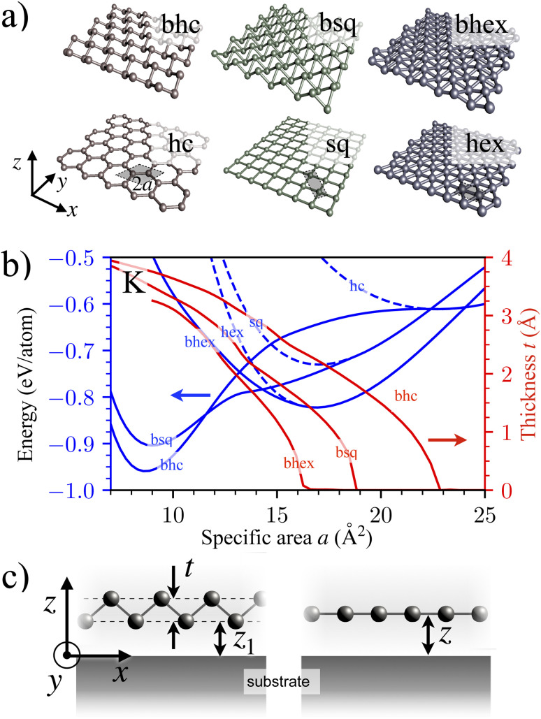 Figure 1
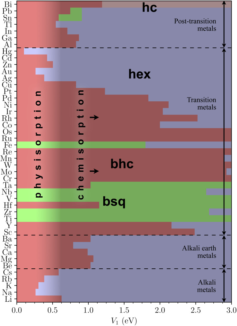 Figure 2
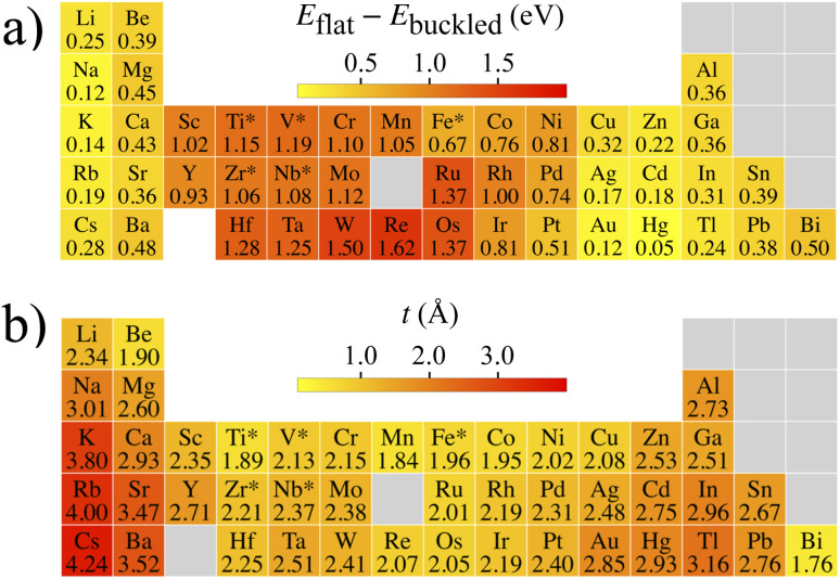 Figure 3
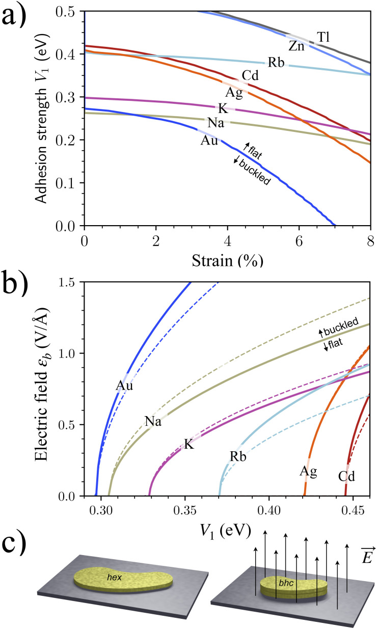 Figure 4
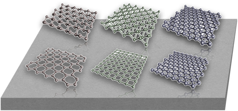 Figure 5
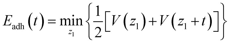 Figure 6
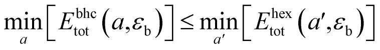 Figure 7
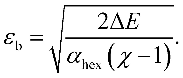 Figure 8
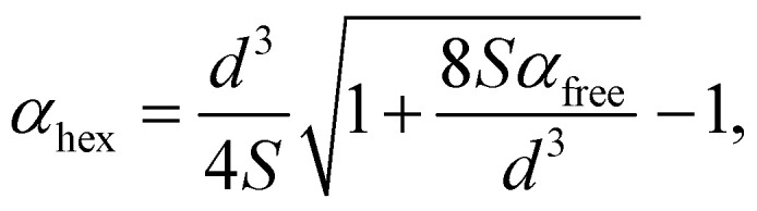 Figure 9
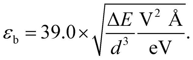 Figure 10
Peer Reviews
No public reviews on file for this paper yet. If you reviewed it on a platform where reviews are public (OpenReview, ICLR, NeurIPS, ICML), you can paste yours below so the community can read it here.
Videos
No videos yet. Explain this paper in a talk, walkthrough, or lecture? Add one.
Taxonomy
TopicsSurface and Thin Film Phenomena · Electron and X-Ray Spectroscopy Techniques · Semiconductor materials and interfaces