Fermi Velocity Dependent Critical Current in Ballistic Bilayer Graphene Josephson Junctions
Amis Sharma, Chun-Chia Chen, Jordan McCourt, Mingi Kim, Kenji Watanabe, Takashi Taniguchi, Leonid Rokhinson, Gleb Finkelstein, Ivan Borzenets

TL;DR
This study explores how the critical current in bilayer graphene Josephson junctions depends on Fermi velocity and gate voltage, offering new tuning possibilities for these devices.
Contribution
The paper demonstrates carrier density dependence of δE in bilayer graphene Josephson junctions, a novel feature compared to single-layer systems.
Findings
The critical current IC follows an exponential trend with temperature: exp(−kBT/δE).
δE increases with gate voltage due to the quadratic dispersion of bilayer graphene.
BGJJs allow tuning of δE through carrier density, unlike single-layer graphene junctions.
Abstract
We perform transport measurements on proximitized, ballistic, bilayer graphene Josephson junctions (BGJJs) in the intermediate-to-long junction regime (L > ξ). We measure the device’s differential resistance as a function of bias current and gate voltage for a range of different temperatures. The extracted critical current IC follows an exponential trend with temperature: exp(−kBT/δE). Here δE = ℏνF/2πL: an expected trend for intermediate-to-long junctions. From δE, we determine the Fermi velocity of the bilayer graphene, which is found to increase with gate voltage. Simultaneously, we show the carrier density dependence of δE, which is attributed to the quadratic dispersion of bilayer graphene. This is in contrast to single layer graphene Josephson junctions, where δE and the Fermi velocity are independent of the carrier density. The carrier density dependence in BGJJs allows for…
Click any figure to enlarge with its caption.
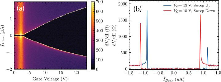 Figure 1
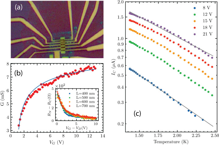 Figure 2
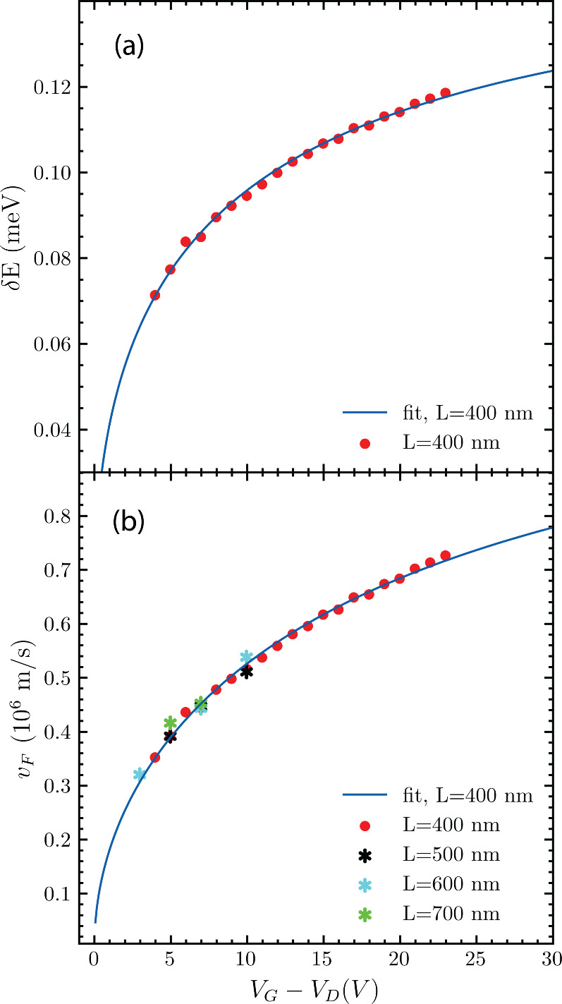 Figure 3
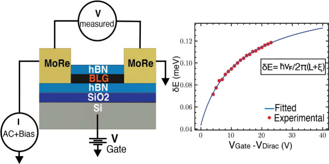 Figure 4
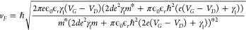 Figure 5
- —National Science Foundation10.13039/100000001
Peer Reviews
No public reviews on file for this paper yet. If you reviewed it on a platform where reviews are public (OpenReview, ICLR, NeurIPS, ICML), you can paste yours below so the community can read it here.
Videos
No videos yet. Explain this paper in a talk, walkthrough, or lecture? Add one.
Taxonomy
TopicsGraphene research and applications · Quantum and electron transport phenomena · Quantum Information and Cryptography
Ballistic graphene Josephson junctions (GJJs) have been widely utilized as a platform to study novel quantum physics phenomena^1,2^ and devices,^3^ including: entangled pair generation,^4,5^ topological states arising from the mixing of superconductivity and quantum Hall states,^6^ as well as photon sensing via bolometry/calorimetry.^7^ Superconductor–normal metal–superconductor Josephson junction (SNSJJ) hosts Andreev bound states (ABS), which carry supercurrents across the normal region of the JJ; in order to enter the ballistic regime, a disorder-free weak link and high transparency at the SN interface are necessary. Hexagonal Boron-Nitride (hBN) encapsulated graphene as a weak link enables highly transparent contacts at the interface while keeping graphene clean throughout the fabrication process.^8^ Here, we study proximitized, ballistic, bilayer graphene Josephson junctions (BGJJs). Bilayer graphene devices (in contrast to monolayer) allow extra potential tunability via a nonlinear dispersion relation, applied displacement field, or lattice rotation.^1^
The critical current (IC) of SNSJJ in the intermediate-to-long regime, where the junction length (L) ≥ superconducting coherence length (ξ_0_), scales with temperature (T) as IC = exp(−kBT/δE). Here, δE = ℏν_F/2πL, an energy scale related to the ABS level spacing.^2,9−13^ Note that in the intermediate regime (L ≈ ξ_0) δE is found to be suppressed.^5^ A previous study of GJJs found that in this regime the relation was held more precisely when ξ was taken into account along with L, that is, δE = ℏν_F/2π(L + ξ).^2,13^ Monolayer graphene displays a linear dispersion relation, which results in a constant Fermi velocity (νF0). Thus, in ballistic GJJs, δE remains independent of the carrier density. In comparison, bilayer graphene displays a quadratic dispersion relation at low energies. In BGJJs we studied, a back-gate voltage (VG) controls the carrier density, and δE dependence on VG_ is observed. Using δE, we extract the Fermi velocity in bilayer graphene: It is seen that ν_F_ increases with VG and saturates to the constant value, ν_F0_, of the monolayer graphene.
Our device consists of a series of four terminal Josephson junctions (on SiO_2_/Si substrate) made with hBN encapsulated bilayer graphene contacted by Molybdenum–Rhenium (MoRe) electrodes. Bilayer graphene is obtained via the standard exfoliation method. It is then encapsulated in hexagonal boron-nitride using the dry transfer method.^14^ MoRe of 80 nm thickness is deposited via DC magnetron sputtering. The resulting device has four junctions of lengths 400, 500, 600, and 700 nm. The width of the junctions is 4 μm. The device is cooled in a Leiden cryogenics dilution refrigerator operated at temperatures above 1 K, and measurements were performed using the standard four-probe lock-in method. A gate voltage VG is applied to the Si substrate with the oxide layer acting as a dielectric, which allows modulation of the carrier density.^2,5,6,15−17^Figure 1(a) displays the differential resistance (dV/dI) map of the 400 nm junction at T = 1.37 K; we see zero resistance (black region) across all applied VG indicating the presence of supercurrent. As the bias current Ibias is swept from negative to positive values, the junction first reaches its superconducting state at a value |Ibias | = IR, known as the retrapping current. Then, as |Ibias| is increased to higher positive values, the junction transitions to the normal state at |Ibias| = IS, known as the switching current. Figure 1(a) shows that the junction can sustain a larger region of critical current as we modulate the carrier density to higher values via VG. Figure 1(b) displays line traces extracted from the dV/dI map which shows hysteresis in IR and IS. This is a commonly observed phenomenon in underdamped junctions^15,18^ or can also be attributed to self-heating.^16,17,19^ The measured switching current IS is slightly suppressed compared to the junction’s “true” critical current IC. However, previous measurements on the statistical distribution of IS in similar graphene devices found that IS is suppressed from IC by no more than 10% for critical currents up to a few μA.^2,20−22^
Extracting the critical current IC from the differential maps for different temperatures, we can see that IC falls exponentially with inverse T (Figure 2c) We also extract the conductance of the junction in the normal regime (IBias ≫ IC). Figure 2(b) shows this conductance (G) for the 400 nm junction device. Due to the significant contact resistance (RC) of the device, the measured conductance G is uniformly suppressed compared to the ballistic limit expectation. However, when accounting for RC within the fit, we find that the conductance G scales as the square-root (as opposed to linearly) of VG (blue curve of Figure 2(b)). This is consistent with ballistic transport.^2,23^ To further demonstrate the ballistic nature of the device, we present normal resistances (RN) of junctions of length 500, 600, and 700 nm with the fitted, constant contact resistance RC subtracted (Figure 2(b) inset). The inset plot shows that the values of RN – RC are independent of the junction length, demonstrating the ballistic nature of the devices.
To extract δE of the junction, we go to the discussion of IC vs the temperature trends in Figure 2(c). Here, the y-axis is plotted in logarithmic scale. From the slope of the curves log(IC) = −(kB/δE)T for each gate, one can extract δE versus VG (plotted in Figure 3a). Unlike for the case of monolayer graphene, a clear dependence on VG is seen (The observed trend further supports the view that our devices operate in the long ballistic regime. Diffusive Josephson junctions are governed by the Thouless energy (22,24) which does not match the trend with respect to VG seen in Figure 3(a)). The energy δE scales linearly with the Fermi velocity vF (Figure 3(b)). Note that calculating vF from δE for junctions in the intermediate regime requires knowledge of the superconducting coherence length ξ. In the fit discussed below, we use ξ’s dependence in vF.
We now compare the experimentally obtained δE (and vF) to the theoretical expectation. With the dispersion relation for bilayer graphene written as , we get the expression for the Fermi velocity: .^25−27^ Here, γ_1_ = 0.39 eV a parameter describing the interlayer coupling,^25^k is the momentum wavevector, and m* is the effective mass of electrons. Moreover, the Fermi energy for bilayer graphene scales as . The carrier concentration n, controlled by the applied gate voltage VG, is given by with VD as the gate voltage at the Dirac point. The total capacitance CTotal is a combination of quantum capacitance Cq and gate oxide capacitance Cox: . The quantum capacitance Cq for bilayer graphene is determined by , where e is the electron charge. The gate oxide capacitance per unit area is , where ϵ_0_ is the vacuum permittivity, ϵ_r_ is the relative permittivity of the oxide, and d is the thickness of the oxide layer. For a silicon oxide gate with d = 300 nm we get Cox ≈ 115 μF/m^2^. Thus, the full expression for the Fermi velocity vF is
Note that the effective mass m* typically ranges from 0.024 me to 0.058 me for 1 × 10^12^ ∼ 4 × 10^12^ carriers/cm^2^,^28^ where me is the electron rest mass. Experimental data provides us with the following: . We also note that ξ has a dependence on vF and the superconducting gap Δ: ξ = ℏvF/2Δ.^13^ To fit δE, the model is set as where m*, Δ, VD, and d are the fitting parameters and VG is the independent variable. (We use the as-designed length of the device L and take ϵ_r_ = 3.9 for SiO_2_.)
The resulting fits of the data from the 400 nm junction for δE and vF are plotted as solid lines in Figure 3(a) and Figure 3(b) respectively. Moreover, taking the fitted parameters from Table 1, we calculate the Fermi velocity vF for the available data points of all other junctions on the same substrate. As seen from Figure 3(b), the calculated vF of all devices is in good agreement with the fit obtained from the 400 nm junction (this is as expected for devices on the same substrate as long as they have consistent parasitic doping and a superconductor–graphene contact interface). The fitted parameters are summarized in Table 1. All fall within the range of expected values, with Δ being consistent with previously measured values for graphene/MoRe junctions.^2^ Furthermore, using the values obtained from the model, we find that vF saturates to the value of 1.1 × 10^6^ m/s as VG tends to infinity.
In conclusion, we study the evolution of the critical current with respect to the gate in bilayer graphene Josephson Junctions (BGJJs). Using the critical current-temperature relation expected for intermediate-to-long junctions, we extract the relevant energy scale δE and find that it has a clear gate dependence. As δE is proportional to the Fermi velocity vF in bilayer graphene, we are able to match the observed gate dependence to the theoretical expectation. Our observation is contrasted with monolayer graphene JJs, which do not have a gate-dependent δE. This result showcases the greater tunability of BGJJs, and offers additional avenues for device characterization. Although not observed here, it should be possible to engineer Josephson junctions that transition from the short to the intermediate/long ballistic regimes in situ via gate voltage. The ability to tune ABS level spacing could have applications in self-calibrating sensors, or for matching resonance conditions in multiterminal superconducting devices.
The reference list from the paper itself. Each links out to its DOI / PubMed record.
- 1Park G. H.; Lee W.; Park S.; Watanabe K.; Taniguchi T.; Cho G. Y.; Lee G. H. Controllable Andreev Bound States in Bilayer Graphene Josephson Junctions from Short to Long Junction Limits. Phys. Rev. Lett. 2024, 10.1103/Phys Rev Lett.132.226301.38877917 · doi ↗ · pubmed ↗
- 2Borzenets I. V.; Amet F.; Ke C. T.; Draelos A. W.; Wei M. T.; Seredinski A.; Watanabe K.; Taniguchi T.; Bomze Y.; Yamamoto M.; Tarucha S.; Finkelstein G. Ballistic Graphene Josephson Junctions from the Short to the Long Junction Regimes. Phys. Rev. Lett. 2016, 117, 23700210.1103/Phys Rev Lett.117.237002.27982627 · doi ↗ · pubmed ↗
- 3Kroll J. G.; Uilhoorn W.; van der Enden K. L.; de Jong D.; Watanabe K.; Taniguchi T.; Goswami S.; Cassidy M. C.; Kouwenhoven L. P. Magnetic field compatible circuit quantum electrodynamics with graphene Josephson junctions. Nat. Commun. 2018, 10.1038/s 41467-018-07124-x.PMC 621847730397206 · doi ↗ · pubmed ↗
- 4Chen W.; Shi D. N.; Xing D. Y. Long-range Cooper pair splitter with high entanglement production rate. Sci. Rep. 2015, 10.1038/srep 07607.PMC 515458725556521 · doi ↗ · pubmed ↗
- 5Borzenets I. V.; Shimazaki Y.; Jones G. F.; Craciun M. F.; Russo S.; Yamamoto M.; Tarucha S. High Efficiency CVD Graphene-lead (Pb) Cooper Pair Splitter. Sci. Rep. 2016, 10.1038/srep 23051.PMC 478978926971450 · doi ↗ · pubmed ↗
- 6Amet F.; Ke C. T.; Borzenets I. V.; Wang J.; Watanabe K.; Taniguchi T.; Deacon R. S.; Yamamoto M.; Bomze Y.; Tarucha S.; Finkelstein G. Supercurrent in the quantum Hall regime. Science 2016, 352, 966–969. 10.1126/science.aad 6203.27199424 · doi ↗ · pubmed ↗
- 7Lee G.-H.; Efetov D. K.; Jung W.; Ranzani L.; Walsh E. D.; Ohki T. A.; Taniguchi T.; Watanabe K.; Kim P.; Englund D.; Fong K. C. Graphene-based Josephson junction microwave bolometer. Nature 2020, 586, 42–46. 10.1038/s 41586-020-2752-4.32999482 · doi ↗ · pubmed ↗
- 8Dean C. R.; Young A. F.; Meric I.; Lee C.; Wang L.; Sorgenfrei S.; Watanabe K.; Taniguchi T.; Kim P.; Shepard K. L.; Hone J. Boron nitride substrates for high-quality graphene electronics. Nat. Nanotechnol. 2010, 5, 722–726. 10.1038/nnano.2010.172.20729834 · doi ↗ · pubmed ↗