Novel APD Array Configurations for Improved Detection Area and Frequency Response
Xuan Zeng, Xuzhen Yu, Hewei Zhang, Yi Lu, Yanli Zhao

TL;DR
This paper introduces new APD array designs that improve detection area and bandwidth, surpassing the limitations of traditional photodetectors.
Contribution
The paper proposes two novel APD array configurations that enhance bandwidth while increasing detection area.
Findings
One APD array achieved a 780 MHz bandwidth, a 1.41 times improvement.
Another array reached 1.21 GHz bandwidth, a 1.35 times improvement.
Structure 2 outperformed Structure 1 with lower noise and better SNR.
Abstract
This paper presents two novel avalanche photodiode (APD) array structures designed to significantly enhance both detection area and bandwidth, overcoming the common trade-off between these parameters in conventional photodetectors. The impact of various parameters on the bandwidths of the two distinct array structures was theoretically simulated. Experimental validation using the self-fabricated 2 × 2 array on PCB board confirmed the bandwidth enhancement realized through inductor integration, with one APD array demonstrating an increase to 780 MHz (1.41 times greater) and another showing an increase to 1.21 GHz (1.35 times greater). Unlike prior works where array bandwidth is often lower than single detectors, our structures maintain high bandwidth while expanding the detection area. Structure 2 is particularly recommended over Structure 1 because of its lower noise, better…
Genes, proteins, chemicals, diseases, species, mutations and cell lines named across the full text — each resolved to its canonical identifier and authoritative record.
Click any figure to enlarge with its caption.
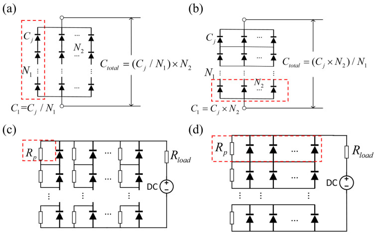 Figure 1
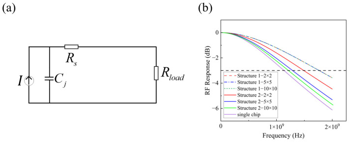 Figure 2
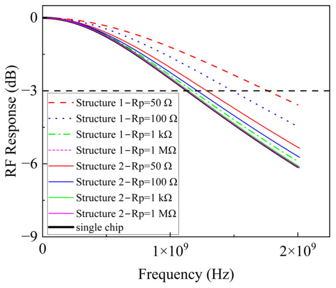 Figure 3
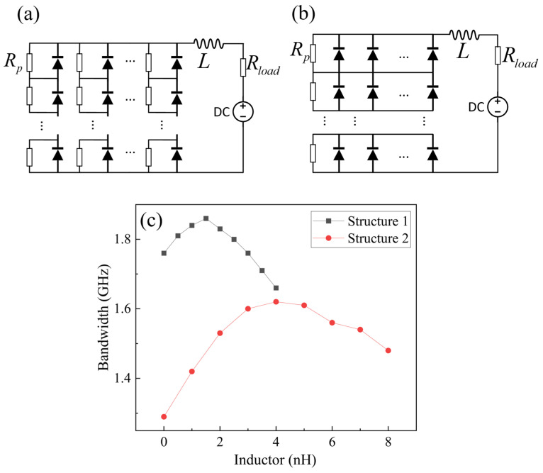 Figure 4
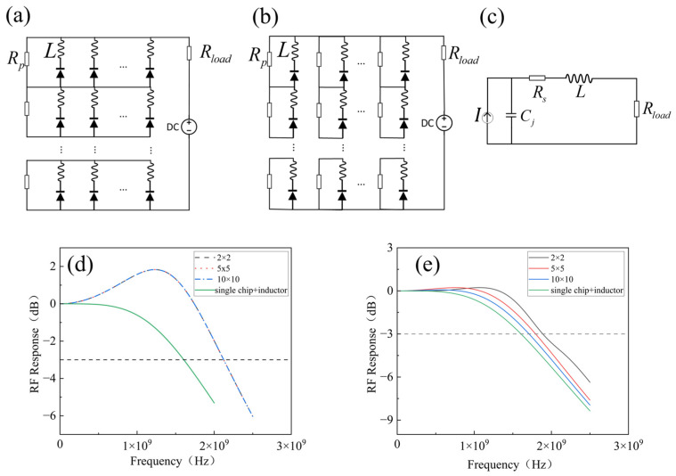 Figure 5
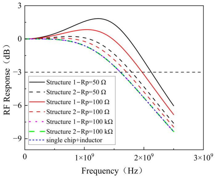 Figure 6
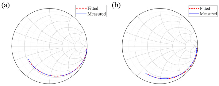 Figure 7
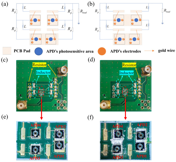 Figure 8
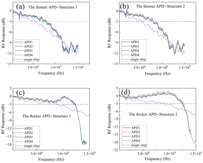 Figure 9
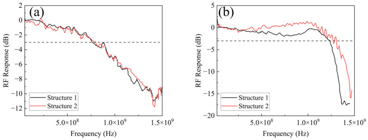 Figure 10
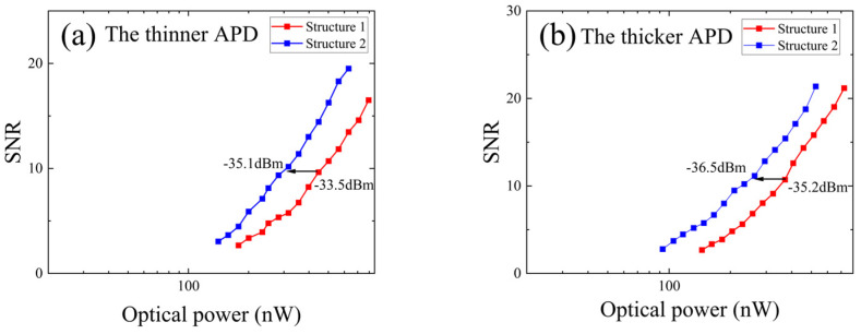 Figure 11
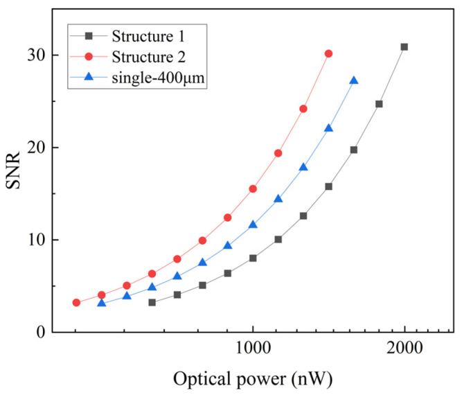 Figure 12
 Figure 13
- —National Key Research and Development Program of China
- —Science and Technology Project from Wuhan City
Peer Reviews
No public reviews on file for this paper yet. If you reviewed it on a platform where reviews are public (OpenReview, ICLR, NeurIPS, ICML), you can paste yours below so the community can read it here.
Videos
No videos yet. Explain this paper in a talk, walkthrough, or lecture? Add one.
Taxonomy
TopicsAdvanced Optical Sensing Technologies · Advanced Photonic Communication Systems · Photonic and Optical Devices
1. Introduction
Developing high-performance photodetectors with both large detection areas and high-speed responses remains a critical challenge in contemporary optoelectronics. With the growing demand of higher data rates and larger detection areas in applications such as free space optical communication [1,2,3,4,5,6], lidar [7,8,9], and medical imaging [10,11], the performance requirements for photodetectors have become increasingly stringent. Recent advancements in material systems and device architectures have opened new avenues for optimizing photodetector performance [6,12]. Unfortunately, traditional photodetectors tend to face a trade-off between the expanded detection areas and bandwidth. To overcome this limitation, high-speed photodetector arrays are strongly desired instead of single photodetectors with large detection areas [13,14,15].
To date, research on single-output photodetector arrays with large detection areas has been scarce. One study introduced a Si/Ge avalanche photodiode (APD) array that utilized pixel interconnects, achieving a bandwidth of 142 MHz for each pixel, which was reduced to 52 MHz post-cascading [16,17]. In another instance, a Si/Ge APD array with a pixel diameter of 33 μm provides a 9 GHz bandwidth for a single APD, with a gradual decrease to 6.7 GHz, 1.2 GHz, 0.7 GHz for 2 × 2, 5 × 5, 10 × 10 arrays, respectively [18]. A 4 × 4 PIN PD array designed for optical wireless receivers has been reported to have a bandwidth of 1 GHz per PD, which is reduced to 610 MHz after packaging [19]. Furthermore, an InAlAs/InGaAs APD array utilized as a position-sensitive detector in free-space optical communication maintains a bandwidth of 1.8 GHz for a single APD, which diminishes to 1 GHz when configured as a 3 × 3 array [5]. A high-speed 8 × 8 InGaAs/InP PIN array for free-space optical systems, with a pixel diameter of 40 μm and the detection area of 0.4 mm × 0.4 mm, achieves a uniform bandwidth of 8.5 GHz across the 8 × 8 array, matching the bandwidth of the individual pixels [14]. For the array discussed, as array size increases, the bandwidth tends to decrease or remain constant without additional measures to improve it.
While inductive peaking has been extensively studied for single photodetectors [20,21,22,23], its application to photodetector arrays remains unexplored. Traditional photodetector arrays often suffer from bandwidth degradation as the detection area increases, limiting their performance in high-speed application. This paper addresses this challenge by proposing two novel APD array structures that not only maintain a large detection area but also achieve significant bandwidth enhancement through strategic inductor integration. In the simulation section, two diverse array structures are proposed and the influence of array size, parallel resistors, and inductors on the array bandwidth of both array types is investigated. In the experimental section, exploratory 2 × 2 arrays for two distinct structures are fabricated using two APDs with different absorption layer thicknesses. The arrays were tested for bandwidth, power consumption and signal-to-noise ratio to provide a comprehensive evaluation of their performance. This work may provide new perspectives for achieving higher bandwidths in large-scale arrays.
2. Structures of Two-Dimensional Photodiode Arrays
The fundamental aim of a two-dimensional photodiode array is to enlarge the detection area without degrading the bandwidth, which is a critical requirement for high-speed optoelectronic applications. As the detection area of an individual photodetector expands, the junction capacitance increases, leading to an extended RC time constant and resulting reduction in the bandwidth. To address the trade-off between bandwidth and detection area, a single large-area photodetector was transformed into an array composed of multiple smaller photodetectors. The key is to interconnect these small detectors such that the bandwidth of the array remains unaffected by the enlargement of the detection area.
Figure 1 illustrates two distinct array structures: one where pixels are initially connected in series and then in parallel (Structure 1, see Figure 1a), and another where the order is reversed, connecting in parallel before series (Structure 2, see Figure 1b). When the array has an equal number of rows and columns (i.e., ), the total capacitance of both structures is equivalent to that of a single photodetector. Consequently, both array designs have the potential to expand the detectable area, while maintaining a high-frequency response.
In practical applications, there is a possibility that the incident light spot may not fully cover the entire photodetector array. This can lead to photodetectors in the non-illuminated regions remaining in a high-resistance state, effectively interrupting the photocurrent flow. To avoid this scenario, parallel resistors ( ) were introduced into both array structures to establish a path for the photocurrent (see Figure 1c,d).
3. Theoretical Simulation and Analysis of Photodetector Arrays
3.1. Array’s Bandwidth
In standard photodetector applications, a fixed load resistor of 50 Ω is added (referred to as a single chip, see Figure 2a). For both array structures, the effect of the array size (N × N) on the bandwidth was initially analyzed. Assuming a junction capacitance of 2 pF, the series resistor for a single photodetector was set to 20 Ω, with the array’s parallel resistor at 50 Ω in the simulations. As shown in Figure 2b, for Structure 1, the array bandwidth is independent of the array size, consistently exceeding the bandwidth of a single photodetector. In the case of Structure 2, the bandwidth shows a gradual decline with an increase in the array size, but it still remains higher than the bandwidth of a single chip. Under the condition of an equal array size, Structure 1 has a higher bandwidth than Structure 2. This is primarily because Structure 1 introduces a smaller additional resistance compared to Structure 2.
In addition to the array size, it is important to consider the influence of the values on the array bandwidth. A 5 × 5 array served as an example in the simulation that investigated the bandwidth variation with different values across both array structures. As shown in Figure 3, the bandwidths for both structures decreased as the increased. When the was much higher than the load resistor (50 Ω), the bandwidth for both structures was the same as that of a single chip.
3.2. Optimization of the Array Structure
The bandwidth of a single photodetector can be enhanced by integrating it with an inductor, transforming its equivalent circuit from a simple RC circuit to an RLC circuit [22,23,24]. To raise the array bandwidth, the introduction of inductors into the array structure is considered. First, an inductor was added at the end of the array to control the bandwidth, as shown in Figure 4a,b. The bandwidths for both array structures were simulated with = 2 pF, = 20 Ω, = = 50 Ω, and the resulting graphs showing how the bandwidth varies with inductance are presented in Figure 4c.
By employing this approach, the bandwidth of Structure 1 can be enhanced from 1.76 GHz to 1.86 GHz, an increase of 1.06 times. Similarly, for Structure 2, the bandwidth can be improved from 1.29 GHz to 1.62 GHz, which is a 1.26-fold increase. Thus, the influence of the inductor on bandwidth optimization is more effective in Structure 2 than Structure 1. However, it does not surpass the optimal bandwidth enhancement achieved by a single detector integrated with an inductor, which is 1.44 times greater [20].
Another approach for placing inductors within the array is to add an inductor to each cell within the array to control its bandwidth. The structures of both arrays are illustrated in Figure 5a,b. The circuit configuration for tuning the bandwidth of a single photodetector with an inductor (single chip + inductor) is shown in Figure 5c. When changing the size of the array, the simulation settings remained the same, with = 2 pF, = 20 Ω, = = 50 Ω. It can be observed that Structure 1 maintains a constant bandwidth (See Figure 5d). For Structure 2, the bandwidth decreased with the expansion of the array, gradually approaching the bandwidth of the single chip + inductor scenario (See Figure 5e).
Furthermore, following the introduction of inductors, the impact of varying the on the bandwidth of both array structures was studied. As depicted in Figure 6, for both structures, an increase in corresponds to a reduction in bandwidth. With a smaller value, Structure 1 has a greater bandwidth than Structure 2. However, when is much larger than the fixed 50 Ω load resistance, the bandwidth of both Structure 1 and Structure 2 match, becoming equivalent to the bandwidth of a single chip + inductor.
Although the array can achieve a higher bandwidth when is set to 50 Ω, in actual applications, power consumption issues must also be considered. Numerous parallel resistors of the array may result in considerable power loss. For an APD operating at a higher reverse bias voltage, it is advisable to use a resistor with a higher resistance value for . This strategy enables the array to maintain a bandwidth exceeding that of a single chip while simultaneously maintaining a lower level of power consumption.
4. Experimental Results of Inductor-Integrated APD Arrays
4.1. APD Parameter Extraction
Optimizing the bandwidth of photodetectors equipped with inductors requires precise determination of the photodetector’s series resistance . The ideal inductance can be calculated as follows [20]:
Typically, the values of and can be obtained by measuring the scattering parameters ( ) of the photodetector and fitting them to its equivalent circuit model [25,26]. Two InGaAs/InAlAs APDs with a diameter of 200 μm and a uniform structure but varying absorption layer thicknesses developed in our laboratory are referred to as the thinner APD (1 μm) and the thicker APD (2 μm) [27]. Figure 7a,b shows the measured and fitted curves (from 20 MHz to 1 GHz), respectively. For the thinner APD, and are extracted to be 5.01 pF and 10.98 Ω; for the thicker APD, and are extracted to be 2.79 pF and 12.60 Ω.
With the fitted values of and , the most effective inductance for the thinner APD and the thicker APD can be calculated to be 9.3 nH and 5.5 nH, respectively, as determined by Equation (1). Because of the absence of inductors with these exact values in our laboratory, an 8.5 nH inductor was used for the thinner APD, and a 7 nH inductor was utilized for the thicker APD in the follow-up experiments.
4.2. Array Fabrication
To verify the feasibility of the two array structures, 2 × 2 arrays for both structures were fabricated by externally integrating resistors and inductors on a PCB board. Figure 8a,b is the schematic diagram of the PCB boards for Structure 1 and Structure 2, respectively.
The APD chips were equipped with a single N-electrode at the back and a pair of P-electrodes alongside another N-electrode at the front. Attachment of these chips to the PCB pads was achieved through the application of conductive silver adhesive. This adhesive not only ensured the stable positioning of the chips but also established an electrical link with the N-electrodes, ensuring proper functioning within the structure. Additionally, gold wire bonding was employed to link the P-electrodes to the pads. Figure 8c,d depicts the actual PCB boards corresponding to the two array structures, where Figure 8e,f shows the physical sections of the chips for both structures. It should be noted that despite the variations in thickness, the thinner and thicker APDs used in the experiment were visually identical.
4.3. Power Consumption and Frequency Response
Considering the high operating voltage of the APD, with the thinner APD operating at 28 V and the thicker APD at 45 V, to reduce the power consumption, an value of 500 kΩ was utilized in the experiments. During operation, the thicker 2 × 2 arrays consumed 18.5 mW for Structure 1 and 9.2 mW for Structure 2. On the other hand, the thinner 2 × 2 arrays used 6.3 mW for Structure 1 and 3.1 mW for Structure 2. The power consumption of these arrays was considerably lower than that array reported previously [14]. Compared with Structure 1, Structure 2 reduced the array’s power consumption owing to its fewer resistors.
During the testing process, the incident light was focused onto a single APD within the array, and bandwidth measurements were performed on all the four APDs to verify the uniformity of the array. The bandwidth curves derived from the experiments are depicted in Figure 9, and the detailed data are listed in Table 1. The test results reveal that both the thinner and thicker APDs demonstrate satisfactory uniformity across the four APDs within the two array structures, and the bandwidths of Structure 1 and Structure 2 are consistent. It can be inferred that the results of the experiments correspond to those of the simulations.
Specifically, for the thinner APD, the single chip bandwidth is 556 MHz, while the bandwidth for the 2 × 2 arrays in both Structure 1 and Structure 2 ranges from 778 to 790 MHz, about a 1.41-fold increase over the single APD. The thicker APD’s individual bandwidth is 910 MHz, with array bandwidth ranging from 1.21 to 1.25 GHz, about a 1.35 times enhancement compared to the single APD.
In practical applications, incident light may illuminate either a single pixel or multiple pixels within the array. To further strengthen the experimental validation, a new set of measurements was performed. A fiber collimator was used to transform the divergent spatial light from the fiber output into collimated light. The beam diameter was 4.0 mm, which was large enough to fully cover all four APDs in the 2 × 2 array. Based on this, the bandwidth of the array was tested. The test results are shown in Figure 10.
For the thinner APD, Structure 1 achieved a bandwidth of 775 MHz, while Structure 2 reached 790 MHz. For the thicker APD, the bandwidths of Structure 1 and Structure 2 were measured to be 1.23 GHz and 1.27 GHz, respectively. These values align closely with the bandwidths measured under single-APD illumination, conclusively demonstrating that the proposed array structures enhance the entire array’s bandwidth. This further validates the effectiveness of the design in maintaining high-speed performance while expanding the detection area.
4.4. Signal-to-Noise Ratio
The Signal-to-Noise Ratio (SNR) is a crucial parameter for receivers and was measured using similar methods previously reported in our laboratory [27]. The noise performance of the 2 × 2 APD arrays with varying absorption layer thicknesses, is presented in Table 2. Structure 2 consistently exhibits reduced noise levels compared to Structure 1 for both APD types. This reduction in noise is largely owing to the simplified design of Structure 2, which employs a smaller number of resistors, leading to a decrease in circuit noise.
The SNR was calculated by comparing the output signal pulse amplitude with the measured noise amplitude. These comparisons were made in response to a series of narrow signals from a signal generator at varying light power levels. The relationship between the SNR and input light power for the two types of APDs and their different arrays was assessed, and the results are presented in Figure 11. At an SNR of 10, the optical power required for Structure 1 is −33.5 dBm for the thinner APD, surpassing that of Structure 2 by 1.6 dB. Similarly, for the thicker APD, Structure 1 demands an optical power of −35.2 dBm, which is 1.3 dB more than Structure 2. Thus, for both types of APDs, Structure 2 exhibits a higher SNR than Structure 1 under equivalent incident light power, primarily because of the lower noise levels in Structure 2.
For the photodetector array, the bandwidth, power consumption, and signal-to-noise ratio performance all need to be considered in practical applications. While Structure 1 has higher bandwidth than Structure 2 when the parallel resistance is small, larger values are preferred in practice to reduce power consumption. Under this condition, the bandwidths of both structures become similar. Structure 2 is recommended due to its lower power consumption and better SNR performance, resulting from fewer resistors in the circuit.
The array device will ultimately be utilized as a standalone device. Consequently, it is necessary to compare the APD array with a single APD of identical detection area. Due to the absence of a single APD with a photosensitive diameter of 400 μm and similar structure, we consider simulating the SNR performance of a 2 × 2 array composed of four APDs, each with a photosensitive diameter of 200 um, and a single APD with a 400 um diameter. The simulation parameters are based on the performance characteristics of the thicker APD, as measured in experiments, such as a responsivity of 0.9 A/W, a gain of 10 (see Appendix A and Figure A1), and an avalanche coefficient of 0.27. As shown in Figure 12, the single APD exhibits inferior SNR performance compared to Structure 2. Considering that the detector can be modeled as an RC circuit, which attenuates signals, the transfer function is given by the following equation, where f represents the signal frequency and B denotes the detector bandwidth.
Given that the 2 × 2 array has a broader bandwidth compared to the single APD, the signal attenuation by the single APD intensifies as the frequency of the transmitted signal rises. As a result, the SNR of the single APD declines more quickly than that of the detector array.
5. Conclusions
In this study, two novel photodetector array structures were designed, fabricated, and comprehensively characterized, and these structures successfully overcome the traditional trade-off between detection area and bandwidth. Through the integration of inductors, for the thinner and the thicker APD, the 2 × 2 arrays achieved a bandwidth increase of 1.41 times and 1.35 times, respectively, compared to their single APD. Especially, low power consumption was achieved for both array structures, with the power consumption for the two APDs in Structure 1 being 18.5 mW and 6.3 mW, and for Structure 2 being 9.2 mW and 3.1 mW, respectively. Moreover, the SNR performance of Structure 2 is superior to Structure 1 and that of a single APD with the same detection area. Based on these results, Structure 2 is particularly recommended because of its simplified circuitry, lower power consumption and superior SNR performance, making it a more advantageous structure for large-area photodetector arrays. These findings indicate the potential application value of these new detector arrays in high-speed free space optical communications.
Although the experimental section only verifies the performance of the 2 × 2 arrays, it is inferred from the simulation results that these structures are also applicable to larger and higher speed arrays. The array device in this paper is a combination of independent devices. Future research will investigate integrating spiral inductors on photodetector electrodes with photodetector arrays on a single chip to enhance the duty cycle and enable miniaturization of the array. Furthermore, the integration of lenses will be considered to enhance the responsivity of the array.
The reference list from the paper itself. Each links out to its DOI / PubMed record.
- 1Czylwik A. Array-Type High-Speed and Large Detection Area Integrated Wireless Optical Receiver Proceedings of the 2021 XXXI Vth General Assembly and Scientific Symposium of the International Union of Radio Science (URSI GASS)Rome, Italy 28 August–4 September 202113
- 2Umezawa T. Kusakata K. Kanno A. Matsumoto A. Yamamoto N. Kawanishi T. Large Active Area, High-Speed Photoreceiver for Optical Wireless Communications Proceedings of the 2018 International Topical Meeting on Microwave Photonics (MWP)Toulouse, France 22–25 October 201814
- 3Zhang R. Hu N. Zhou H. Zou K. Su X. Zhou Y. Song H. Pang K. Song H. Minoofar A. Turbulence-resilient pilot-assisted self-coherent free-space optical communications using automatic optoelectronic mixing of many modes Nat. Photonics 20211574375010.1038/s 41566-021-00877-w · doi ↗
- 4Song H. Zhang R. Zhou H. Su X. Zou K. Duan Y. Karapetyan N. Song H. Pang K. Hu N. Turbulence-resilient pilot-assisted self-coherent free-space optical communications using a photodetector array for bandwidth enhancement Opt. Lett.2022475723572610.1364/OL.47414937219313 · doi ↗ · pubmed ↗
- 5Ferraro M.S. Clark W.R. Rabinovich W.S. Mahon R. Murphy J.L. Goetz P.G. Thomas L.M. Burris H.R. Moore C.I. Waters W.D. In Al As/In Ga As avalanche photodiode arrays for free space optical communication Appl. Opt.201554 F 182F 18810.1364/AO.54.00F 18226560607 · doi ↗ · pubmed ↗
- 6Ferraro M.S. Rabinovich W.S. Mahon R. Murphy J.L. Clark W.R. Waters W.D. Vaccaro K. Campbell J.C. Position Sensing and High Bandwidth Data Communication Using Impact Ionization Engineered APD Arrays IEEE Photonics Technol. Lett.201931586110.1109/LPT.2018.2882886 · doi ↗
- 7Li Q. Wang C. Wei X. Ye B. Wang S. Chen F. Gong H. Design of non-imaging receiving system for large field of view lidar Infrared Phys. Technol.202313310480210.1016/j.infrared.2023.104802 · doi ↗
- 8Royo S. Ballesta-Garcia M. An Overview of Lidar Imaging Systems for Autonomous Vehicles Appl. Sci.20199409310.3390/app 9194093 · doi ↗