Metalens formed by structured arrays of atomic emitters
Francesco Andreoli, Charlie-Ray Mann, Alexander A. High, Darrick E. Chang

TL;DR
This paper explores using arrays of atomic emitters to create efficient, robust metalenses with complex optical functions.
Contribution
The paper introduces a novel method to design metalenses using structured arrays of atomic emitters with tailored lattice constants.
Findings
Structured arrays of atomic emitters can achieve large transmission with arbitrary phase shifts.
The collective response enhances robustness against losses in the atomic metalens.
Large-scale simulations with N ∼ 5 × 10⁵ atoms demonstrate the feasibility of the design.
Abstract
Arrays of atomic emitters have proven to be a promising platform to manipulate and engineer optical properties, due to their efficient cooperative response to near-resonant light. Here, we theoretically investigate their use as an efficient metalens. We show that, by spatially tailoring the (subwavelength) lattice constants of three consecutive two-dimensional arrays of identical atomic emitters, one can realize a large transmission coefficient with arbitrary position-dependent phase shift, whose robustness against losses is enhanced by the collective response. To characterize the efficiency of this atomic metalens, we perform large-scale numerical simulations involving a substantial number of atoms (N ∼ 5 × 10⁵) that is considerably larger than comparable works. Our results suggest that low-loss, robust optical devices with complex functionalities, ranging from metasurfaces to…
Genes, proteins, chemicals, diseases, species, mutations and cell lines named across the full text — each resolved to its canonical identifier and authoritative record.
Click any figure to enlarge with its caption.
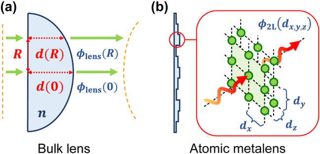 Figure 1
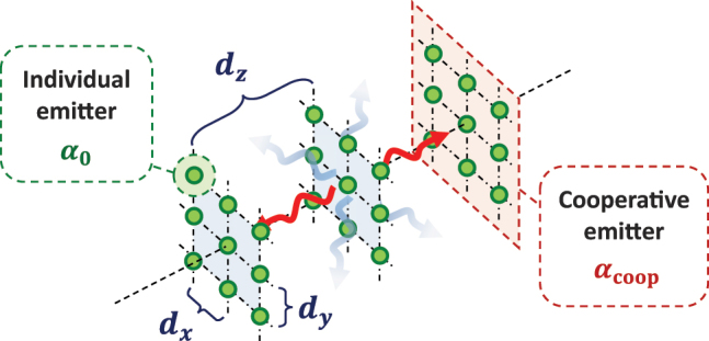 Figure 2
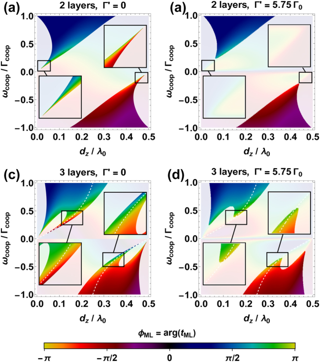 Figure 3
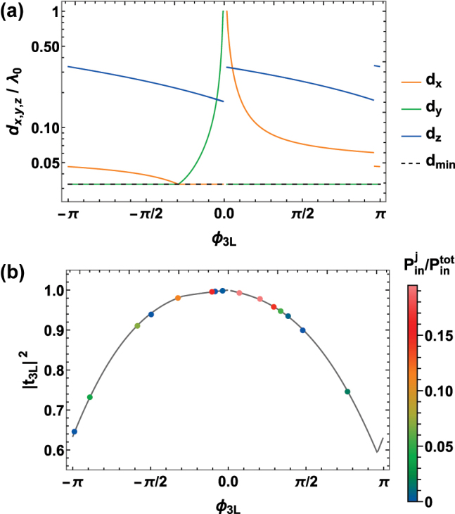 Figure 4
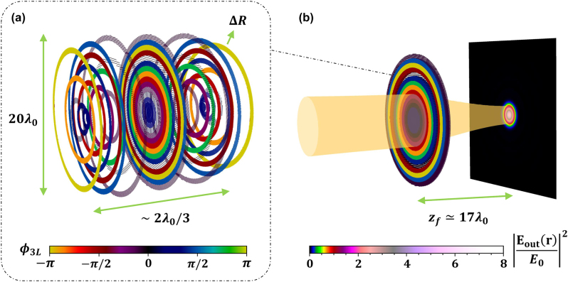 Figure 5
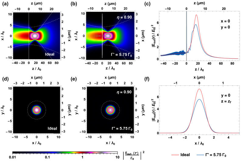 Figure 6
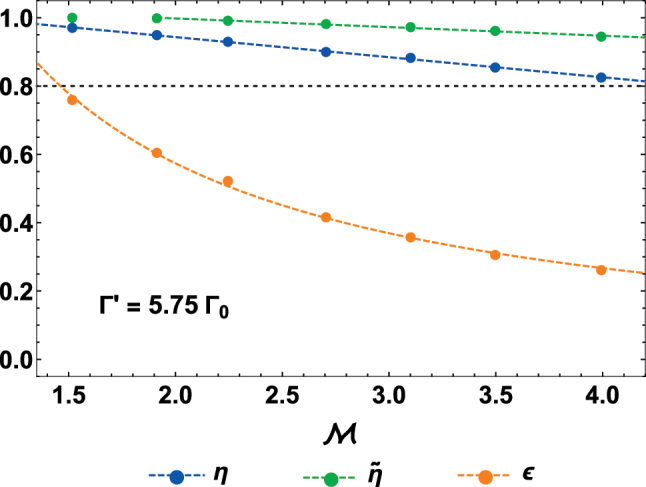 Figure 7
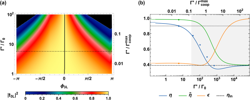 Figure 8
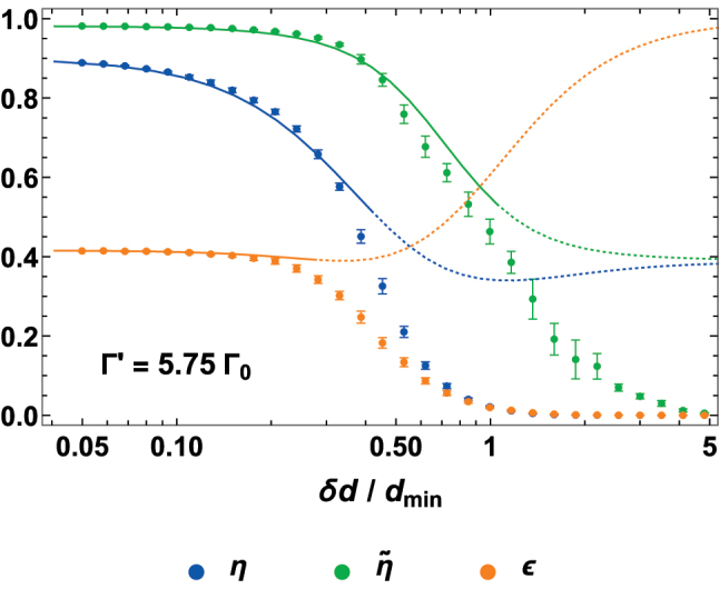 Figure 9
- —HORIZON EUROPE Marie Sklodowska-Curie Actions
- —Generalitat de Catalunya
- —Horizon 2020 Framework Programme
- —European Research Council
- —Government of Spain
- —HORIZON EUROPE European Innovation Council
- —H2020 Marie Skłodowska-Curie Actions
Peer Reviews
No public reviews on file for this paper yet. If you reviewed it on a platform where reviews are public (OpenReview, ICLR, NeurIPS, ICML), you can paste yours below so the community can read it here.
Videos
No videos yet. Explain this paper in a talk, walkthrough, or lecture? Add one.
Taxonomy
TopicsMetamaterials and Metasurfaces Applications · Plasmonic and Surface Plasmon Research · Photonic Crystals and Applications
Introduction
1
Light-mediated dipole–dipole interactions in dense ensembles of atom-like emitters, and the wave interference encoded in them, can lead to a cooperative response that is markedly different from that of an isolated emitter [1], [2]. This resource is most effectively harnessed in ordered arrays of emitters with subwavelength lattice constants, where the collective behavior leads to nontrivial phenomena, including an efficient, directional coupling to light. Capitalizing on these properties, many works have explored classical and quantum optical applications of atomic arrays [3], [4], [5], [6], [7], [8], [9], [10], [11], [12], [13], [14], [15], [16], [17], [18], [19], [20], [21], [22], such as the realization of an atomically thin mirror [23], [24], [25]. Perhaps most relevant to the theme of this paper, these arrays have been proposed to implement various classical optical functionalities, including nonreciprocity [26], optical magnetism [27], [28], [29], wavefront engineering [28], [29], [30], polarization control [31], [32], and chiral sensing [33]. Here, we explore a distinct route toward their application as an optical metalens, which only requires the ability to design the positions of identical emitters.
Metalenses have recently emerged as a promising alternative to traditional bulk optics, enabling complex optical operations while retaining subwavelength thicknesses [34], [35]. Their functionality demands simultaneous control over both transmission intensity and phase pattern. In conventional metasurfaces, this is achieved by spatially varying the size, shape, and orientation of individual nanoscatterers, which generally support both electric and magnetic modes. In contrast, the optical response of atom-like quantum emitters is usually dominated by electric dipole transitions, and it offers limited control over their radiative properties. On the other hand, atomic emitters represent an excellent playground to engineer collective effects, as their electronic transition can provide a low-loss, near-resonant optical resonance, with a large scattering cross section , compared to their point-like, physical size [36]. Inspired by the paradigms of conventional metasurfaces, previous works have proposed to engineer an optical metalens out of a bi-layer atomic array, by locally shifting the resonance frequencies of the individual emitters with additional dressing lasers, whose intensities should vary on a subwavelength scale [28], [29], [30]. A similar approach was also proposed in Ref. [37], involving a disordered sheet of atoms.
With one eye on integrated photonic devices, here we propose a different mechanism to realize an efficient metalens, which only requires a suitable choice of the positions of solid-state, atom-like emitters. Specifically, we demonstrate that one can achieve full control of the transmission phase in a bi-layer, rectangular array, while maintaining unit transmittance, by simply varying lattice constants and layer spacing. Moreover, by adding a third layer, we show that these transmission properties can be robustly maintained even in the presence of nonradiative losses or other imperfections, owing to the enhanced collective response. Finally, we demonstrate that these structures can be used as building blocks of an efficient metalens, which we verify through large-scale numerical simulations involving a substantial number of emitters (up to N ∼ 5 × 10^5^), which is considerably higher than comparable works [38], [39], [40], [41], [42], [43], [44], [45], [46], [47], [48], [49]. The corresponding code is available for public use at Ref. [50], provided with a broader, user-friendly toolbox to simulate the linear optical response of an arbitrary set of two-level, quantum emitters.
The rest of the paper is structured as follows. First, in Section 2, we review the concept of metalenses, and we introduce the physical system under analysis and its theoretical model. Then, in Section 3, we show how arrays of atomic emitters can be engineered to guarantee unit transmission and tunable phase shift. In Section 4, we use these elements to design an illustrative metalens composed of atomic arrays, and in Section 4.1, we test its behavior through extensive numerics, while optimizing its free parameters via a global particle-swarm algorithm [50]. Finally, in Section 4.2, we probe the resistance of that design against different sources of losses or imperfections.
Overview of metalens concept and presentation of our system
2
Conventional refractive lenses rely on local variations of the optical path inside the lens (where light experiences a higher, positive refractive index) to induce a spatially dependent phase shift. Thereby, the wavefront is shaped in such a way that the output beam focuses at a designed distance, as pictorially represented in Figure 1a. In the past couple of decades, however, the novel idea of developing flat metalenses with much smaller footprints has emerged [51], [52], [53], [54], [55]. These metalenses rely on the electromagnetic response of tailored nanostructures to locally impress abrupt phase shifts on the transmitted light [35], [56], [57], [58], while maintaining a thickness on the order of the wavelength or less [34], [35].
*Pictorial comparison between a textbook bulk lens and an atomic metalens. (a) Bulk lens of refractive index n, whose spatially variable optical path d(R) induces a phase delay ϕ lens(R), which curves the incident wavefront, to make it focus at the target distance. (b) Schematic structure of an atomic metalens. Its building blocks consist of at least two atomic arrays in series, whose subwavelength lattice constants d
x,y,z < λ 0 can be engineered to ideally ensure a fully directional transmission, with an arbitrary phase shift. For a realistic, lossy system, three atomic layers are required to enhance the robustness to losses.*
Regardless of physical implementation, the function of a simple ideal lens of focal length f on a monochromatic input beam of light with wavevector is to impart the position-dependent phase profile
upon transmission. This phase is defined modulo 2π, and here we adopt the convention −π ≤ ϕ lens ≤ π. Moreover, we define the transverse coordinate , while the parameter ϕ 0 corresponds to the phase at the center of the lens [53], [59]. Rather than using dielectric or metallic nano-elements to realize this phase, an atomic metalens instead relies on the use of properly positioned, two-level, solid-state emitters (see Figure 1b).
Although the theory that we present will be rather general, from an experimental perspective color centers in diamond can offer a promising framework for its implementation, as they stand out for their excellent optical properties [60]. Specifically, they behave as atom-like emitters with well-defined selection rules and a dipolar response aligned along one of the four possible tetrahedral directions of the diamond lattice [60], [61], [62], [63], [64], [65]. Current fabrication technologies, moreover, offer good control over their spatial position [66], up to nm [67], [68]. At the same time, recent works have explored ways to fix the dipole orientations along a well-defined axis [69], [70], [71], [72] or create exactly one emitter at a target position [73], [74]. Although the full combination of these properties into either 2D [75], [76] or 3D [77] large-scale arrays remains a challenge, recent experimental efforts show promising results toward that direction [74]. Concretely, to achieve high-resolution 3D structures, one can envision a process of patterned ion implantation followed by near-field enhanced laser writing, to deterministically write defects at the desired locations. This would be followed by overgrowth of subsequent array layers [78]. Alternatively, processes utilizing block-polymers can also realize the desired resolution [79]. In principle, all these processes could be modified to create desired arrays of point dipoles.
More specifically, we focus on the case of Silicon Vacancy (SiV) centers, which we model as idealized two-level emitters with resonant frequency 2πc/ω 0 ≈ 737 nm. In this model, we assume that the fabrication process permits to preferentially discriminate over the four possible orientations, so that all the emitters have the same dipole matrix element . Moreover, we characterize these emitters with both a coherent, radiative and elastic scattering rate , and an additional broadening Γ′ ≈ 5.75Γ_0_ which accounts for losses and other deviations from the ideal case. Here, k 0 = 2π/λ 0 = nω 0/c denotes the resonant wavevector within the bulk diamond of refractive index n ≃ 2.4. Further details on the definition of Γ′ are discussed in Appendix A. Although the ratio is relatively low, the optical response of an atomic metalens is protected by the collective behavior, thus allowing for higher efficiencies. To conclude, although we focus on this illustrative level of detrimental broadening, in Sec. IVB, we study the behavior of our system when increasing Γ′ by orders of magnitude.
Global control of transmission
3
We now introduce the theoretical framework to capture the linear optical response of a collection of N quantum emitters in response to a monochromatic classical field, allowing for arbitrary positions. For intensities below the saturation threshold, the nonlinear behavior of a quantum emitter is negligible, and each SiV linearly responds to near-resonant light with a characteristic polarizability , where corresponds to the detuning between the input ω and resonant ω 0 frequencies [80].
The total field at any point in space consists of the sum between the incident field E in(r) and the field rescattered by the atomic emitters, reading
where the dyadic Green’s tensor
defines the scattering pattern of each atomic dipole . For simplicity, the Green’s tensor is computed at the resonant frequency ω 0, making the equations local in time. This approximation is commonly adopted in the context of atomic physics, owing to the small bandwidth of the optical response Γ_0_ ≪ ω 0 [5]. Moreover, this approach becomes exact in the resonant limit of Δ = 0 that will be later considered.
The dipole moments of the emitters are linearly driven by the total field at their position, leading to the self-consistent coupled-dipole equations [81]
which account for the process of multiple light scattering in a nonperturbative fashion. Here, we defined the parameter , while we introduced the input Rabi frequency .
Transmission of M arrays in series
3.1
Our goal is to show how the transverse lattice constants d _ x,y _ and distances d _ z _ of a stack of M ≥ 2, 2D rectangular arrays of atomic emitters can be chosen to impress an arbitrary phase shift, while preserving unit transmission. To do so, it is useful to define the atomic dipoles as p _ mj _, whose double indices identify the positions as , with transverse coordinates .
We first review the cooperative behavior of a single, rectangular 2D array, placed at z = z _ m _. For simplicity, we assume that the input light is a -polarized, plane wave , and we focus on the limit where the arrays infinitely extend in the transverse directions , . Within this regime, any generic solution of Eq. (4) can be written as a superposition of transverse Bloch modes with wavevector q _ xy _. A plane wave at normal incidence, however, only excites the mode with vanishing transverse wavevector q _ xy _ = 0, meaning that all the dipole moments simplify to p _ mj _ = p _ m (q _ xy _ = 0) = p _ m . The whole array, then, cooperatively responds to light as a single, collective degree of freedom, with an effective polarizability α coop = α 0(Δ − ω coop, Γ_coop), characterized by the cooperative decay rate Γ_coop(d _ x,y _) and frequency shift ω coop(d _ x,y _) of the excited mode [23], [24]. Physically, these properties come from the single atoms interacting with the fields generated by all the others in the plane; mathematically, when assuming p _ mj _ = p _ m _ in Eq. (4), one obtains the in-plane contribution , which can be computed with the prescription of Refs. [6], [82], [83].
Once excited, the field coherently scattered by each array can be calculated via Eq. (2). Due to the discrete translational symmetry, the array can add a reciprocal lattice vector to the incident field, where are integers. This results in a set of diffraction orders with total wavevector , where the z-component is since energy is conserved |k ^(a,b)^| = k 0. In the relevant subwavelength regime d _ x,y _ < λ 0, all diffraction orders become evanescent except . This ensures the selective radiance of the array into the same mode of the input light [84], [85], with a cooperative decay rate that scales inversely with the lattice constants, and can thus be significantly greater than the single emitter rate. When stacking M arrays consecutively, the scattered light is then constrained within the normal direction , and each array responds with the same polarizability α coop mentioned before (as pictorially described in Figure 2). At this point, Eq. (4) simplifies into a smaller set of M equations for the dipole amplitudes p _ n _ of each array [16]
where Ω_0_ = Ω_in_(0, 0), while the terms are related to the field scattered by an array at z _ m _ and probed by the array at z _ n _. Its radiative part is given by , while is the sum of the evanescent diffraction orders with imaginary wavevectors , whose value is reported in Appendix B.
*1D, cooperative model for a 3D atomic array, illuminated at normal incidence. We consider a stack of M subwavelength, rectangular 2D arrays of atomic emitters with constant d
x,y , separated by a longitudinal distance d
z . The emitters are identical two-level systems, with a resonant frequency ω 0 and spontaneous emission rate Γ0, which identify the polarizability α 0(Δ = ω − ω 0, Γ0). The layers are illuminated at normal incidence and can scatter light only in this direction (red, wavy arrows), since the other diffraction orders are evanescent (blue, shaded, wavy arrows). Within each 2D array, the optical response is characterized by a single-mode, collective transition, with cooperative resonant frequency ω coop and decay rate Γcoop=3Γ0λ02/(4πdxdy) , characterizing the cooperative polarizability α coop = α 0(Δ − ω coop, Γcoop).*
After solving the set of collective coupled-dipole equations Eq. (5), one can use Eq. (2) to reconstruct the field. Since each array can only selectively radiate into the same mode of the input light, it is straightforward to define the far-field transmission and reflection coefficients [16]
We notice that these equations can be solved without fixing any value of Ω_0_, due to the linearity of the optical response p _ m _ ∝ Ω_0_. Similarly, Eq. (5) can be directly solved for the dimensionless ratios , so that the value of the dipole matrix element does not have to be specified.
To conclude, for the following calculations, we find it favorable to restrict to a regime where the evanescent fields are negligible. For a subwavelength, rectangular lattice, an approximate rule of thumb that guarantees this condition is that all the diffraction orders are at least exponentially suppressed by a factor ∼1/e^2^, which happens when d _ z _ ≳ d _ x,y _/π. As discussed in Appendix B, further caution is required when approaching d _ y _ ∼ λ 0, due to perfect interference effects that make nominally diverge in the limit of infinitely extended 2D arrays.
Phase control
3.2
A metalens is typically composed of nanostructures as wide as ≲λ 0, which transmit the majority of light and impress a tunable phase shift. We now show how the lattice constants of a stack of atomic arrays can be similarly engineered, aiming to use them as the building blocks of an atomic metalens. Hereafter, we define the phase of transmission as ϕ _ ML_ = arg t _ ML_ ∈ (−π, π], and we explicitly focus on the resonant case Δ = 0, although the same method can be extended to near-resonant light.
We begin by considering the simplest scenario, corresponding to a single atomic layer in the lossless regime of Γ′ = 0. The complex value of t 1L depends on the difference between the collective resonance frequency ω coop(d _ x,y _) and the frequency of the incoming light, which we fixed to the resonance frequency of a single emitter (i.e., Δ = 0). In principle, this means that the transmission phase ϕ 1L = arg t 1L is itself tunable via the choice of lattice constants d _ x,y . Nonetheless, using Eqs. (5) and (6), it is easy to show that high transmission and arbitrary phase cannot be achieved with one layer of atoms, as the conditions of reciprocity and energy conservation |t 1L|^2^ + |r 1L|^2^ = 1 impose |t 1L| = cos(ϕ 1L), which limits the phase range to |ϕ 1L| ≤ π/2 and allows unit transmission only in the trivial case of far-detuned driving, where no phase is imprinted ϕ 1L = 0. On the contrary, the largest phase shifts |ϕ 1L| ∼ π/2 are obtained near resonance, where the transmittance drops sharply to zero (i.e., the input field is strongly reflected). Moreover, the range of achievable phases is particularly fragile to the addition of small losses Γ′/Γ_coop ≪ 1, decreasing as .
For an ideal system, we can achieve perfect transmission with arbitrary phase by considering a bi-layer (M = 2) array. As long as , this system is equivalent to a Fabry–Perot cavity, composed of two atomic mirrors with the complex reflectivity r 1L and transmission t 1L mentioned above [33], [86]. In the lossless regime Γ′ = 0, it is well known that such an interferometer ensures unit transmission t 2L = exp(2iϕ 1L) when the distance between the mirrors matches the Airy condition k 0 d _ z _ = πl − arg(r 1L), with [87]. Due to this reason, a proper choice of d _ x,y,z _ allows to keep unit transmission while arbitrarily designing the total phase ϕ 2L = 2ϕ 1L over the full (−π, π] range. This property is represented in Figure 3a, where we independently vary both the subwavelength lattice constants d _ x,y _ and layer spacing d _ z _, plotting ϕ 2L as a function of d _ z _ and the single-layer parameter ω coop(d _ x,y )/Γ_coop(d _ x,y _). As expected, we observe full phase tunability with sufficient transmittance, as quantified by the nonshaded, brightly colored regions where |t 2L|^2^ > 0.5.
*Transmission of a multilayer atomic array, as a function of ω coop(d
x,y )/Γcoop(d
x,y ) and d
z . (a, b) Colorbar representation of the phase shift ϕ 2L = arg t 2L of two atomic layers, given either Γ′ = 0 (a) or Γ′ = 5.75Γ0 (b). The transverse lattice constants are varied within the range λ 0 > d
x,y ≥ d min = 0.03λ 0, which means that Γ′/Γcoop(d
x,y ) ≳ 0.03. When different choices of d
x and d
y are associated to the same value of ω coop(d
x,y )/Γcoop(d
x,y ), the pair with the highest cooperative decay is selected. The region where |t 2L|2 < 0.5 is represented by a white shaded area, while the insets show the relevant case of ϕ 2L ≡ arg t 2L ∼ ±π and |t 2L|2 ≥ 0.5. (c, d) Same structure of subfigures (a) and (b), but for the three-layer case. The white dashed lines represent the chosen branch d
z (d
x,y ) that maximizes the transmittance. Along this path, the insets show that both the phase ϕ 3L = ±π and the transmission |t 3L|2 ≥ 0.5 can be simultaneously obtained over a much broader bandwidth (c), becoming more resistant to the losses (d).*
However, the phase range contracts as in presence of small losses, preventing the achievement of |ϕ 2L| = π, regardless of how small Γ′ > 0 is. As shown by the inset of Figure 3a, this can be related to the asymptotically small bandwidth associated to both |ϕ 2L| ∼ π and |t 2L|^2^ ≥ 0.5 [86], [88], which makes the system more fragile against Γ′. To better quantify this statement, we must first set a minimum interatomic distance d min = 10 nm, whose value is inspired by the discussion of Section 2. This translates into d _ x,y,z _ ≥ d min = 0.03λ 0, which prevents the cooperative response to become arbitrarily large and overtake any sources of broadening Γ′ > 0. In Figure 3b, we then use the conventional value Γ′ = 5.75Γ_0_ of Section 2, observing that both a sufficient transmission |t 2L|^2^ ≥ 0.5 and full phase control can no longer be simultaneously achieved.
In general, M − 1 transparency conditions d _ z _(d _ x,y ) similar to that of a Fabry–Perot cavity can be found for arbitrary values of M [89], and the addition of more atomic layers M > 2 is important to restore the resistance to losses around |ϕ _ ML| ∼ π. This can be intuitively understood for even number of layers M, as a proper choice of d _ z _(d _ x,y _) can make the system act as M/2 cascaded cavities, so that . For odd number of layers M, less intuitive conditions for perfect interference hold, but still we show that M = 3 layers are enough to provide resistance to losses.
To define the proper relations d _ z _(d _ x,y _) between the longitudinal and transverse lattice constants, we introduce a closed-form solution of Eq. (6), which reads [90]
where the function u _ M _(k, d _ z _) = sin(Mkd _ z _)/sin(kd _ z _) relates the finite-size behavior to the dispersion relation k(d _ x,y,z _) = k(ω coop(d _ x,y )/Γ_coop(d _ x,y _), d _ z ) of an infinite chain [16]. In the lossless regime of Γ′ = 0, the unit transmission t _ ML = (−1)^ a ^ exp(iMk 0 d _ z _) is ensured by fixing d _ z _(d _ x,y _) to fulfill k(d _ x,y,z _) = aπ/(Md _ z ), where the natural number a = 1, …, M − 1 identifies the M − 1 possible solutions within the first Brillouin zone. With this choice, the field acquires a total phase shift of ϕ _ ML(d _ x,y _) = Mk 0 d _ z _(d _ x,y _) + aπ with respect to propagation in the bulk environment.
In our M = 3 case, we choose the branch of d _ z _(d _ x,y _) with a = 2, as represented in Figure 3c and 3d by a dashed, white line. When spanning d _ x,y , this is associated to high transmittance and complete phase control, in both the lossless (Figure 3c) and lossy Γ′ = 5.75Γ_0 (Figure 3d) regimes. More specifically, we scan the transverse lattice constants d _ x,y _ along the two straight lines (d _ x _ = d min) ∪ (d min ≤ d _ y _ < λ 0) and (d min ≤ d _ x _ < λ 0) ∪ (d _ y _ = d min), which allows to associate a unique set of spacings d _ x,y,z _ to any value of ϕ 3L(d _ x,y _) = arg t 3L(d _ x,y _, d _ z _(d _ x,y )). This correspondence is represented in Figure 4a, showing that only a limited set of distances λ 0/6 ≤ d _ z _ ≤ λ 0/3 is required, thus implying a maximum thickness of , which translates to for the case of SiV centers. To conclude, in Figure 4b, we explicitly prove that this scheme allows, in presence of broadening Γ′ = 5.75Γ_0, to maintain a sufficient transmittance |t 3L|^2^ > 0.6 for any relevant value of ϕ 3L.
*Lattice constants d
x,y,z and transmittance |t 3L|2 as a function of phase ϕ 3L, given Γ′ = 5.75Γ0. (a) We scan the transverse lattice constants along the two straight lines (d
x = d min) ∪ (d min ≤ d
y < λ 0) and (d min ≤ d
x < λ 0) ∪ (d
y = d min), with d min = 0.03λ 0 (black, dashed line). At the same time, the choice of d
z (d
x,y ) that maximizes the transmittance allows to associate a unique set of lattice constants (colored lines) to any phase ϕ 3L = arg t 3L(d
x,y , d
z (d
x,y )) (horizontal axis). (b) Transmittance |t 3L|2 as a function of the phase ϕ 3L (gray line). The colored points are associated to the rings composing the illustrative atomic metalens discussed in Section 4. Their colors are associated to the relative power of the input light over their area, i.e., Pinj∝∫Rj−1Rj|Ein|2dR .*
We notice that those phases within the interval of 0 ≲ ϕ 3L ≲ 0.01π cannot be engineered, due to the limited value of max ω coop ≈ 28Γ_coop_ for d min ≤ d _ x,y _ ≤ λ 0. Nonetheless, for practical applications such as a metalens, this range can be approximated with exactly ϕ 3L = 0 (i.e., no emitters), as its span is negligible compared to typical discretization scales.
Atomic metalens
4
To design an atomic metalens out of three-layer atomic arrays, one needs to spatially tune the lattice constants d _ x,y _, to make the phase shift ϕ 3L(d _ x,y ) match that of an ideal lens, i.e., the value ϕ lens(R) specified in Eq. (1). To define a concrete recipe, we divide the transverse plane into concentric rings j = 1, 2… of radius R _ j _ = jΔR (see Figure 5a), and we associate to each ring the central phase shift ϕ _ j _ ≡ ϕ lens(R _ j−1/2 + R _ j _/2), by using Eq. (1). Here, we recall that the initial phase ϕ 0 is a free parameter. At this point, we impose and extract the lattice constants by numerically inverting the solid line of Figure 4a. The transparency condition of Figure 4b can then be used to define the longitudinal constant . The final metalens is then the union of these discrete building blocks, as shown in Figure 5. By choosing ΔR ≲ λ 0, we ensure a discretization scale with the same order of magnitude of that of usual metalenses [34].
*Structure of an atomic metalens, with focal length f = 20λ 0 and radius R lens = 10λ 0. (a) 3D representation of the atomic metalens, where each point depicts the position of one atom. This atomic metalens is composed of 15 concentric rings of thickness ΔR ≈ 2λ 0/3, with a buffer-zone parameter α ≈ 0.2. The lens has a width of Δz ≈ 2λ 0/3, much thinner than the total diameter of 20λ 0. The atoms belonging to the j-th ring have the same lattice constants dx,y,zj , which are uniquely associated to the phase shift ϕ
j = ϕ lens(ΔR(2j − 1)/2) of Eq. (1) (with ϕ 0 ≃ −2.06), through the curves ϕj=ϕ3Ldx,yj and dzj=dzdx,yj shown in Figure 4. The color of the atoms in each ring reflects the value of ϕ
j , as described by the colorbar at the bottom. (b) Focusing of a x^ -polarized, resonant, input Gaussian beam with w 0 = 4λ 0, by the action of the atomic metalens. The orange, shaded area shows the textbook beam waist w(z) during the focusing process. The metalens is designed to focus the beam at a distance z
f ≃ 17λ 0. This defines the focal plane, where we numerically reconstruct the total relative intensity |E out(R, z
f )/E 0|2 via the input–output formalism of Eq. (2), in the lossy regime of Γ′ = 5.75Γ0. The value of |E out(R, z
f )/E 0|2 is portrayed with the color scheme shown by the colorbar at the bottom. Further results from the coupled-dipole simulations are shown in Figure 6.*
At the interface between the finite rings, the abrupt change of lattice constants can potentially scatter light into unwanted diffraction modes. To soften these detrimental effects, in the -plane we introduce a small buffer zone between two consecutive rings, with atoms placed at intermediate positions. These zones extend over the first fraction 0 ≤ α ≤ 1/2 of each ring, and their definition is not strict, with many possible variants. Our approach is described in Appendix C, and we numerically associate it to a small efficiency increase, up to an additional factor in the estimated efficiency.
To conclude, we remark that for each target focal length f, our atomic metalens is defined up to three free parameters, which are an overall phase shift −π < ϕ 0 ≤ π, the ring thickness d min ≪ ΔR ≲ λ 0, and the buffer fraction 0 ≤ α ≤ 1/2.
Numerical simulations
4.1
To check our design, we want to estimate the efficiency of an atomic metalens with focal length f and centered around z = 0. To this aim, we fix the atomic positions, and we illuminate the system at normal incidence with a -polarized, resonant, input Gaussian beam focused at z = 0, which has beam waist w 0 and focal intensity |E 0|^2^ (see Appendix D). We then perform exact simulations of the linear optical response, reconstructing the total field E out(R, z) via Eqs. (2) and (4). We want to compare it with the theoretical prediction of the field transmitted by an ideal, thin lens of focal length f. This is given by the Gaussian beam E _ f _(R, z), characterized by the beam waist , the focal position , and the focal intensity . Here, the parameter is the so-called magnification of the lens, which quantifies the focusing ability and ensures the conservation of energy ∫|E _ f _|^2^dR = ∫|E in|^2^dR ∝ P in.
To characterize the metalens performance, we quantify the fraction η = P _ η _/P in of power P _ η _ that is correctly transmitted into the target, ideal Gaussian mode E _ f _, divided by the total input power P in [91]. Operatively, this efficiency can be obtained by analytically projecting E out into the target mode E _ f _, namely η = |⟨E _ f _|E out⟩|^2^. This projection has a simple, closed-form expression, which is detailed in Appendix D. Another quantity of interest is the overlap between the transmitted field and the input field ϵ = |⟨E in|E out⟩|^2^. Obviously, one would aim to operate in a regime where η ∼ 1, while ϵ ≪ 1, with the latter inequality signifying that the lens performs some non-negligible transformation. Finally, we notice that, for certain applications, the main requirement is the identification of the focal spot over the background of transmitted light. In view of that, we define the signal-to-background ratio , which divides the power transmitted into the target mode P _ η _ by the total transmitted power P t, rather than by the total input power. Here, one has P _ η _ = ηP in, while P t ∝ ∫|E out|^2^dR is numerically computed from the total field at the focal plane z = z _ f _.
To show the potential of our scheme, we can now discuss an illustrative full-scale simulation of a metalens with focal length f = 20λ 0 and radius R lens = 10λ 0, illuminated by an input Gaussian beam of waist w 0 = 4λ 0. In this illustrative scenario, the ideal magnification would read , associated to an ideal intensity enhancement of . These simulations involve a substantial number of atoms N ∼ 5 × 10^5^, and the techniques by which we accomplish this result are described in the Methods. All the codes are written in Julia [92] and are available at Ref. [50]. The free parameters ΔR ≈ 2λ 0/3, ϕ 0 ≃ −2.06, and α ≈ 0.2 are chosen to maximize η in the lossy regime Γ′ = 5.75Γ_0_. This was first accomplished via a brute-force optimization and then confirmed through a particle-swarm, global-optimization algorithm [50].
The numerical results are shown in Figure 6, where we plot the relative intensity of the total field |E out(R, z)/E 0|^2^, calculated on the horizontal plane y = 0 (top row) and at the expected focal plane z = z _ f _ ≃ 17λ 0 (bottom row). The column on the left (Figure 6a and 6d) shows the ideal values that one would expect for a textbook, ideal lens, i.e., E _ f (R, z). This is compared to the numerical simulations of the atomic metalens, calculated for the lossy case Γ′ = 5.75Γ_0 (right column, Figure 6b and 6e). Very similar plots are obtained when studying the lossless case Γ′ = 0, or when plotting the intensity on the plane x = 0.
*Illustrative case of an atomic metalens with focal length f = 20λ 0, radius R lens = 10λ 0, and parameters ΔR ≈ 2λ 0/3, ϕ 0 ≈ −2.06, and α ≈ 0.2, illuminated by a resonant Gaussian beam with waist w 0 = 4λ 0. The figures show the relative intensity of the total field |E out(R, z)/E 0|2, calculated on the planes y = 0 (top row, subfigures a, b) and z = z
f ≃ 17λ 0 (bottom row, subfigures d, e). The subplots (a, d) represent the ideal case of a textbook lens, while the subplots (b, e) show the results of the numerical simulations with Γ′ = 5.75Γ0. The dashed, white lines represent the ideal value of the beam waist w(z), while the dot-dashed, white lines show the waist of the input beam if no lens were present. The efficiency of the lossy Γ′ = 5.75Γ0 case, estimated from the simulations, reads η ≃ 0.90, while the signal-to-background ratio reads η~>0.98 . The number of simulated atoms is N ≃ 4.6 × 10⁵. Finally, the subplots (c, f) show two line-cuts of the intensity profile, along either the z axis in the x = y = 0 plane (c) or the x axis in the y = 0, z = z
f plane (f). This quantity is depicted for both the ideal (dashed, red line) and lossy (solid, blue line) cases. The gray area in subfigure (c) depicts the space occupied by the atomic metalens.*
We benchmark the optical response of the atomic metalens from our simulations, finding an efficiency η ≃ 0.95 and an intensity enhancement at the focal point of |E out(0, z _ f )/E 0|^2^ ≃ 6.03, in the lossless regime of Γ′ = 0. Similarly, in the lossy case of Γ′ = 5.75Γ_0, we obtain the values η ≃ 0.90 and |E out(0, z _ f )/E 0|^2^ ≃ 5.60. This value can be appreciated in Figure 6c and 6f, where we compare the ideal (red, dashed line) and numerical (blue, solid line) field intensity along, respectively, either the z axis (in the x = y = 0 plane) or the x axis (at the focal plane). These high efficiencies stand out when considering the much lower overlap ϵ ≃ 0.42 between the output field and the input beam, which means that the atomic metalens is nontrivially acting on the input beam. Finally, both the lossy and the lossless cases exhibit a high signal-to-background ratio, reading . To understand how the broadening Γ′ = 5.75Γ_0 affects the efficiency, we recall from Figure 4b that the transmittance |t 3L|^2^ highly depends on ϕ 3L, meaning that some rings can transmit more light than others. Considering our illustrative metalens, the complex transmission associated to each ring is represented with a colored point in Figure 4b. The overall reduction of the efficiency due to the losses (i.e., the ratio between the lossy Γ′ > 0 and lossless Γ′ = 0 efficiencies) agrees well with the average transmittance |t 3L(ϕ _ j _)|^2^ of the rings, each weighted by the relative power of the input light illuminating their area (corresponding to the color of the points in Figure 4b). Notably, this intuitive model explains why the efficiency η can strongly depend on the choice of ϕ 0.
Although the atomic metalens was designed to operate for resonant light at Δ = 0, a similar reasoning allows to qualitatively predict the spectral bandwidth where the efficiency remains high. To show this, we calculate the cooperative decay rates for all the rings that compose the metalens and weight them by the corresponding fraction of input light, to define the average value (of the order of for SiVs [93], [94]). As detailed in Appendix E, we observe that the efficiency remains as high as η ≳ 0.8 as long as , while quickly decreasing outside.
To conclude, it is interesting to investigate how the response is modified when increasing the focusing ability of the lens, as quantified by the magnification . Specifically, in Figure 7, we fix w 0 = 4λ 0 and scan different focal lengths f, plotting the efficiency η (blue points) and the signal-to-background ratio (green points) as a function of . Here, the maximum magnification is associated to the limit k 0 w _ f _ ≫ 1 imposed by the paraxial approximation, while the choice of w 0 = 4λ 0 represents the largest beam waist that we can compute, due to the numerical complexity of the simulation. In presence of broadening Γ′ = 5.75Γ_0_, we observe that the efficiency remains as high as η ≳ 0.82 (dotted, black line) up to , where the overlap with the input field is as low as ϵ ≈ 0.26. Overall, we find the empirical scalings of , , and (colored dashed lines). Assuming that these scalings would hold true for larger values of w 0, they would predict efficiencies as high as η ≈ 0.5 up to (where the overlap with the input field is as low as ϵ ≈ 0.08), and signal-to-background ratios larger than up to (where ϵ ≈ 0.02).
Efficiency of an atomic metalens as a function of the magnification, given Γ′ = 5.75Γ0. We fix both the waist of the input beam to w 0 = 4λ 0, and the radius of the lens R lens = 10λ 0, while showing the efficiency η (blue points), signal-to-background ratio η~ (green points), and input-field overlap ϵ (orange points) as a function of the magnification 1≤M≲w0/λ0=4 . For each point, we perform a particle-swarm optimization of the free parameters ϕ 0, α, and ΔR to maximize the efficiency η [50]. By fitting the data, we infer the empirical scalings η≈1.06−0.06M , η~≈1.05−0.03M and ϵ≈−0.04+1.23/M (colored, dashed lines). The black, dotted line shows the reference value of 0.8.
Losses and imperfections
4.2
Up to now, the presence of experimental losses and imperfections has been modeled by the addition of a detrimental broadening Γ′ ≈ 5.75Γ_0_, whose value was chosen to qualitatively capture some key properties of state-of-the-art experiments with color centers in diamond. While our studies up to now represent an optimistic scenario, here we investigate the performance of the metalens as the broadening rate Γ′ increases, or when the atoms are subject to increasing spatial disorder.
First, we study the resistance to increasing levels of broadening Γ′, which we compare with the maximum cooperative decay rate allowed in the system. To this aim, it is instructive to focus on the single building blocks of the metalens. In Figure 8a, we show the relation between the phase ϕ 3L (on the horizontal axis) and transmittance |t 3L|^2^ (color scheme), when considering increasing values of Γ′ (vertical axis, in log scale). This corresponds to the extension of Figure 4b (which coincides with the black dashed line in Figure 8a) to arbitrary values of Γ′. Notably, when , some phases cannot be realized anymore (black areas in the plot). We recall that the addition of further atomic layers is expected to drastically increase the resistance to losses, although presenting the drawback of adding more atomic emitters, and increasing the overall thickness of the metalens. Reducing the minimum lattice constant d min would similarly work, by increasing the maximum cooperative rate .
*Resistance to nonradiative losses. (a) Transmission of a three-layer array, given increasing levels of Γ′. Similarly to Figure 4b, we use our definition of d
x,y,y to associate a unique transmittance |t 3L|2 (color scheme) to any target phase ϕ 3L (horizontal axis). We then vary Γ′ (vertical axis) to track the change in the transmittance. We notice that an almost identical plot is obtained when numerically optimizing the choices of d
x,y,z ≥ d min = 0.03λ 0 to maximize transmittance, proving the validity of our scheme. The black, dashed line highlights the particular case Γ′ = 5.75Γ0. The black areas (bounded by dotted, white lines) identify regions of the parameter space that cannot be obtained with any choice of d
x,y,z . (b) Efficiency as a function of Γ′, given an atomic metalens with focal length f = 20λ 0, radius R lens = 10λ 0, and construction parameters ΔR ≈ 2λ 0/3, ϕ 0 ≈ −2.06, and α ≈ 0.2, illuminated by a Gaussian beam with w 0 = 4λ 0. The lines show the efficiency η (blue), signal-to-background ratio η~ (green), input-field overlap ϵ (orange), and base-line efficiency η in = |⟨E
f |E in⟩|2 (black, dashed line). The colored, dotted lines represent the values at Γ′ = 0, while the colored points show the case of Γ′ = 5.75Γ0. The black, dotted line depicts a threshold value of 0.9, while the shaded, gray region portrays the regime where some phases cannot be engineered anymore, corresponding to the appearance of black areas in subfigure (a). Finally, the blue asterisks show the efficiencies in case the structural parameters ΔR, ϕ 0, and α are changed to be optimal for the corresponding value of Γ′.*
To get further insights, it is instructive to explicitly focus on the illustrative atomic metalens of Figure 6, with focal length f = 20λ 0, radius R lens = 10λ 0, and parameters ΔR ≈ 2λ 0/3, ϕ 0 ≃ −2.06, and α ≈ 0.2. In Figure 8b, we discuss the overall response of this metalens, for broadening levels up to . The blue line depicts the efficiency η, the orange line the input-field overlap ϵ, and the green line the signal-to-background ratio . Roughly, the system becomes ineffective above the threshold . Notably, the efficiency remains acceptable η ≳ 0.7 as long as Γ′ ≳ 60Γ_0_ although, in principle, this corresponds to a regime where some phases around |ϕ| ∼ π cannot be engineered anymore (gray, shaded region). At the same time, the signal-to-background ratio remains relatively high up to much higher losses, so that up to and up to . We note that these efficiencies are calculated for a fixed choice of ΔR, ϕ 0, and α, which are optimal only for Γ′ = 5.75Γ_0_. This reasoning well describes a situation where the amount of losses is unknown. On the other hand, higher efficiencies (blue asterisk in Figure 8b) are obtained by choosing optimal parameters tailored on the broadening Γ′, as computed via particle-swarm optimization [50].
Finally, we discuss the effect of disorder in the atomic positions, defined by randomly displacing each atomic emitter inside a 3D sphere of radius δd, with a uniform distribution. In Figure 9, we represent with colored points the same quantities of Figure 8b, as a function of increasing disorder δd. As intuitively expected, when the displacement is comparable to d min, then the efficiency is strongly undermined, with η ∼ 0. In that regime, the transmitted light is so randomly altered, that it does not overlap anymore with the input field either, and one gets ϵ ∼ 0. Nonetheless, we notice that the signal-to-background ratio exhibits more robust properties, with up to δd ∼ 0.7d min. We relate these results to the overall drop of transmitted light that occurs in the disordered regime.
Resistance to additional position disorder. The data are calculated for the atomic metalens with focal length f = 20λ 0, radius R lens ≃ 9λ 0, and construction parameters ΔR ≈ 2λ 0/3, ϕ 0 ≈ −2.06, and α ≈ 0.2, illuminated by a Gaussian beam with w 0 = 4λ 0. The horizontal axis represents the random displacement radius δd in units of the minimum lattice constant d min. The points represent the average efficiency (η, blue), signal-to-background ratio ( η~ , green), and overlap with the input beam (ϵ, orange). Each point is calculated by averaging over 10 random configurations, and the error bars represent one standard deviation. The simulation is performed for the lossy case Γ′ = 5.75Γ0. The lines represent the theoretical prediction when replacing the random displacement with the additional inelastic rate ∼2.5Γdis′(δd,dmin)=2.5(π/2)(δd/dmin)2Γcoopmax , where the numerically inferred prefactor stems from the additional complexity of the metalens, compared to stacks of infinite arrays.
As detailed in Appendix A.2, small displacements in a 2D array (or in a stack of arrays) can be well described by a supplementary broadening , whose scaling ensures the dependence of the optical response only on the relative displacement . For the more complex case of an atomic metalens, we numerically find that the position disorder can be still characterized by a supplementary rate , where the empirical prefactor can be attributed to the more fragile interference patterns involved in the metalens response, as well as to the attempt of capturing the overall behavior of different rings with only one unique rate, calculated for d _ x,y _ = d min. To show this, we consider a metalens with perfect spatial positioning but with an additional broadening rate , and we then use the results of Figure 8b to obtain the curves shown in Figure 9. As long as the displacement is small (solid part of the curves), these approximated predictions are in good agreement with the numerical points.
Discussion
5
Complete wavefront shaping requires the simultaneous achievement of high transmittance and full phase control. Usually, metamaterials achieve these requirements by engineering the local properties of the individual scatterers, such as, for example, the shape of nanoresonators. Solid-state, atom-like emitters, however, do not provide the same manufacturing flexibility, and theoretical proposals of atom-based metasurfaces rely on external drives with subwavelength intensity profiles to locally change the emitter properties [28], [29], [30], [37]. Still, the possibility of engineering a complex optical response by solely implanting atomic-scale scatterers in a solid-state environment represents an interesting perspective on device integration and miniaturizability [95], especially when considering the thick substrate that is usually required by standard metasurfaces (typically [34]).
In this work, we showed that stacks of two or more consecutive arrays of solid-state emitters can be engineered to fulfill the necessary requirements of transmittance and phase control, by only choosing proper lattice constants that ensure their correct collective response. Via large-scale numerical simulations [50], we argued that these elements can be combined as the building blocks of a metalens, whose efficiency is robust to losses and other imperfections, due to the collective enhancement of the optical response. This is achieved within a maximum thickness of , which might be potentially reduced even further, by properly addressing the more complicated regime of evanescent interactions. Notably, the perfect tunability of these building blocks and the possibility of their combination can in principle guarantee arbitrary wavefront shaping, which suggests the extension of this mechanism to more articulated applications, such as phase-only holograms [96].
The core design of our atomic metalens is based on an analytic map between any discretized phase pattern and the corresponding set of lattice constants. Although this scheme is intrinsically scalable, the design is complete only up to three macroscopic free variables, given by the overall phase shift ϕ 0 of the metalens, the discretization size of the rings ΔR, and the fraction α of “buffer zones”. The scalability of this optimization step is not trivial, as it involves large-scale coupled-dipole simulations. To facilitate it, one possible strategy would consist of investigating whether each ring made of discrete atoms could be modeled by smooth, flat mirrors, with proper transmission and reflection coefficients. This would enable simulation via optical commercial software, with a computational complexity decoupled from the number of dipoles [97], [98], [99], [100], [101]. Alternatively, it would be interesting to explore if a target, collective optical response could be obtained with far fewer emitters, by inverse-designing their positions through proper optimization algorithms [102]. Some preliminary numerical simulations suggest that adjoint methods might be a promising path in this direction [103].
With our scheme, the total efficiency is protected by the collective response, even if the losses of the individual scatterers are non-negligible Γ′ ≫ Γ_0_. Similar considerations apply beyond the case of atom-like emitters, to any set of optical scatterers with a well-defined resonant, dipolar response, and a ratio between scattering and total cross section equating [36]. This would be the case of plasmonic nanoparticles, for example, which are indeed known to become more resistant to their intrinsic losses when collectively (i.e., nonlocally) responding to light in a 2D, subwavelength array [104]. Our work, based on the idea of combining different arrays together, can then provide additional insights and tools to the context of nonlocal metasurfaces [105].
Finally, it is interesting to mention some specific features of color centers in diamond, whose two-level nature provides nontrivial properties both at the classical and at the quantum level. For example, an atomic metalens based on SiVs would be extremely narrowband and polarization sensitive, finding possible applications in terms of spectral filtering [106], [107], [108], tunability [109], or polarization control [110], [111]. Furthermore, color centers are highly saturable objects, due to their intrinsic nonlinearity, and this behavior would automatically limit the metalens response up to a threshold intensity of light.
At the quantum level, it is known that color centers can be embedded inside a metasurface to enhance some of their functionalities, for example as single-photon sources [112]. It would be interesting to explore if enhanced, collective properties of an ensemble of color centers could be more easily designed by engineering the emitters to act as a nonlocal metasurface. Some evidence exist, for example, that stacks of two atomic arrays can exhibit enhanced nonlinear correlations [86]. More generally, a metasurface based on color centers could provide a possible playground for the emerging contexts of quantum metasurfaces [113] and quantum holography [114], [115].
Methods: We numerically simulate the optical response of the system by solving the coupled-dipole equations of Eqs. (2) and (4), whose computational time scales as ∼N ^3^, where N is the number of atomic dipoles. The input Gaussian beam must have a waist w 0 much smaller than the radius R lens of the atomic metalens, to avoid scattering from the edges or a non-negligible fraction of light passing outside the lens. Due to the paraxial approximation, however, this imposes the constraint λ 0 ≪ w 0 ≪ R lens. Furthermore, to counteract the effects of the broadening Γ′, one must work with small lattice constants down to d min ≈ 0.03λ_0_, thus explaining the necessity of simulating up to N ∼ 5 × 10^5^ atomic dipoles. To accomplish this task, we exploit the fact that the system is symmetric for and , which implies that the each dipole d _ j _ is equal to those of the atoms at the mirrored positions. The actual degrees of freedom are given by the number of atoms satisfying x _ j _ ≥ 0 and y _ j _ ≥ 0, which are roughly . The coupled dipole equations can be then simplified by accounting only for these atoms, and then considering as if each of them scattered light from the mirrored positions as well. A supplementary problem is the amount of Random Access Memory (RAM) needed to perform the simulation. We design the code in such a way that the maximum allocation of memory is given by the construction of the Green’s function matrix. By defining it as a matrix of Complex{Float32} (64 bit) rather than the custom Complex{Float64} (128 bit), we cut the memory consumption to – 300 GB of RAM. We checked that we were still working with enough numerical precision, by comparing the simulations of smaller systems, performed with both choices of the variable definition. Finally, the overall computational time was sped up by using the native, multicore implementation of linear algebra in Julia as well as its vectorized treatment of tensor operations [92], while other relevant computations were split over multiple threads. More information is available in the Github repository provided at Ref. [50].
The reference list from the paper itself. Each links out to its DOI / PubMed record.
- 1Gross M. Haroche S. Superradiance: an essay on the theory of collective spontaneous emission Phys. Rep. 935301396198210.1016/0370-1573(82)90102-8 · doi ↗
- 2Sheremet A. S. Waveguide quantum electrodynamics: collective radiance and photon-photon correlations Rev. Mod. Phys. 951015002202310.1103/revmodphys.95.015002 · doi ↗
- 3Jenkins S. D. Ruostekoski J. Controlled manipulation of light by cooperative response of atoms in an optical lattice Phys. Rev. A 863031602201210.1103/physreva.86.031602 · doi ↗
- 4Facchinetti G. Jenkins S. D. Ruostekoski J. Storing light with subradiant correlations in arrays of atoms Phys. Rev. Lett. 11724243601201610.1103/physrevlett.117.24360128009199 · doi ↗ · pubmed ↗
- 5Asenjo-Garcia A. Exponential improvement in photon storage fidelities using subradiance and “selective radiance” in atomic arrays Phys. Rev. X 7331024201710.1103/physrevx.7.031024 · doi ↗
- 6Perczel J. Photonic band structure of two-dimensional atomic lattices Phys. Rev. A 966063801201710.1103/physreva.96.063801 · doi ↗
- 7Manzoni M. T. Optimization of photon storage fidelity in ordered atomic arrays New J. Phys. 20883048201810.1088/1367-2630/aadb 74PMC 676004231555054 · doi ↗ · pubmed ↗
- 8Guimond P. O. Subradiant bell states in distant atomic arrays Phys. Rev. Lett. 1229093601201910.1103/physrevlett.122.09360130932531 · doi ↗ · pubmed ↗