Rational strategy for power doubling of monolithic multijunction III-V photovoltaics by accommodating attachable scattering waveguides
Shin Hyung Lee, Hyo Jin Kim, Jae-Hyun Kim, Gwang Yeol Park, Sun-Kyung Kim, Sung-Min Lee

TL;DR
A new method using waveguides with scattering elements boosts the power output of multijunction solar cells by nearly 93%.
Contribution
A cost-effective waveguide design with BaSO4 Mie scattering elements is introduced to significantly enhance solar cell output power.
Findings
Maximum output power of 26%-efficient cells increased by ~93% with optimal scattering waveguide integration.
Supplementary tests validated waveguide size effects and arrayed cell performance improvements.
Rear illumination drawbacks were assessed to guide future design optimizations.
Abstract
While waveguide-based light concentrators offer significant advantages, their application has not been considered an interesting option for assisting multijunction or other two-terminal tandem solar cells. In this study, we present a simple yet effective approach to enhancing the output power of transfer-printed multijunction InGaP/GaAs solar cells. By utilizing a simply combinable waveguide concentrator featuring a coplanar waveguide with BaSO4 Mie scattering elements, we enable the simultaneous absorption of directly illuminated solar flux and indirectly waveguided flux. The deployment of cells is optimized for front-surface photon collection in monofacial cells. Through systematic comparisons across various waveguide parameters, supported by both experimental and theoretical quantifications, we demonstrate a remarkable improvement in the maximum output power of a 26%-efficient cell,…
Genes, proteins, chemicals, diseases, species, mutations and cell lines named across the full text — each resolved to its canonical identifier and authoritative record.
Click any figure to enlarge with its caption.
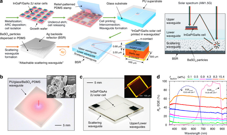 Figure 1
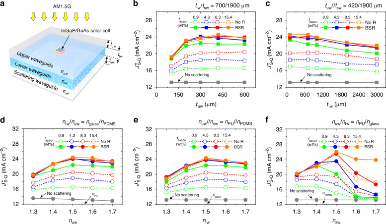 Figure 2
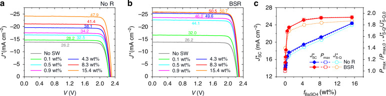 Figure 3
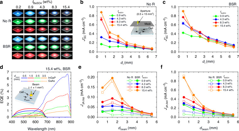 Figure 4
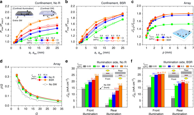 Figure 5
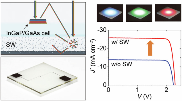 Figure 6
- —https://doi.org/10.13039/501100003662Ministry of Trade, Industry and Energy, Korea | Korea Evaluation Institute of Industrial Technology (KEIT)
- —https://doi.org/10.13039/501100003725National Research Foundation of Korea (NRF)
Peer Reviews
No public reviews on file for this paper yet. If you reviewed it on a platform where reviews are public (OpenReview, ICLR, NeurIPS, ICML), you can paste yours below so the community can read it here.
Videos
No videos yet. Explain this paper in a talk, walkthrough, or lecture? Add one.
Taxonomy
Topicssolar cell performance optimization · Semiconductor Quantum Structures and Devices · Chalcogenide Semiconductor Thin Films
Introduction
Monolithic multijunction III-V compound semiconductor solar cells are widely recognized as ultrahigh-performance photovoltaics, stemming from their favorable material properties such as direct bandgap, high carrier mobility, low-temperature coefficient, and superior radiative hardness^1–5^. These types of solar cells are simply configured into two-terminal photovoltaics without an increase in parasitic absorption loss, which is a practically attractive feature as the complexity of photovoltaic module implementation can be reduced^6,7^. Despite such compelling features, their high manufacturing cost has been a hurdle for the broad application in terrestrial photovoltaics^8^. One direct approach for improving their cost-effectiveness might be reducing materials consumption. This case can be achieved by designing minimal epitaxial stacks (e.g., lattice-matched structures) or reusing growth wafers (e.g., epitaxial lift-off process)^9–11^. Alternatively, an indirect approach to addressing this issue involves improving cell utilization by increasing power generation capability with light concentrators^12–14^. A concentrator intensifies the solar photon flux incident to solar cells, thus enabling solar cells to generate the boosted output power beyond a value available under unconcentrated illumination. However, the typical light concentrators comprising optics components are not actually cost-effective because of the sophisticated module assembly level and the essential maintenance system. Moreover, they do not operate properly under diffuse sunlight, impeding their effectiveness in reducing the levelized cost of electricity.
In contrast, waveguide-based light concentrators do not diminish the cost-reduction benefits due to simple module construction. The waveguide concentrator consists of a transparent multimode slab waveguide containing luminescent, scattering, or both elements capable of redirecting photon propagation^15–22^. By diverting photons towards solar cells embedded within the waveguide or mounted at the waveguide edges through total internal reflection, photon concentration becomes possible without the need for precise module construction. Its effective operation under diffusely incident sunlight is another notable advantage of the waveguide concentrator. Despite these advantages, the waveguide concentrator has not been considered a promising option for reinforcing multijunction or other two-terminal tandem solar cells^6,23,24^. This is due to several concerns regarding performance synergy. While the multijunction cells, typically designed as monofacial cells, require front-side photon incidence to achieve a balanced output current from series-connected subcells, the bifacial cell is an effective configuration to capture photons traveling within the waveguide. Additionally, as multijunction cells are designed to operate efficiently across the entire solar spectrum, the waveguide concentrator with spectral elements responding to a narrow photon spectrum (e.g., luminophores) may not be effective with them. Rigorous tuning of spectral elements in the waveguide concentrator can alleviate the ineffectiveness of their finite spectrum responses^6^; however, the level of output power amplification still remains limited, thus necessitating the development of more advanced waveguide concentrator technology compatible with high photovoltaic-capable multijunction cells.
In this regard, the present study introduces a straightforward yet effective approach to amplifying the output power of multijunction III-V solar cells by employing a simply combinable waveguide concentrator. Microscale InGaP/GaAs double-junction solar cells are arranged within a transparent slab medium through the transfer-printing assembly method, where the cell deployment is optimized to enhance front-surface photon collection, both for directly incident solar flux and waveguided solar flux. To enable broad-spectrum solar photons to be waveguided^20–22^, we separately prepare a photon scattering medium of a sticky elastomer slab with BaSO_4_ particles and attach it underneath the cell-incorporated transparent waveguide slab. The key features of the present approach are (i) the optimal integration design of multijunction cells with waveguides to concentrate broadband photon flux preferentially on the front cell surfaces and (ii) the simplicity of module implementation that allows considerable augmentation of the multijunction cell output power without the need for complicated process addition. Based on experimental characterization and numerical modeling, systematic investigations to access photon waveguide and collection properties at various waveguide parameters and scattering element conditions are conducted to find the maximum benefits of waveguide concentrators with multijunction III-V solar cells.
Results
Module design and fabrication
Figure 1a schematically depicts the proposed module design and its fabrication steps. The module comprises two-terminal microscale InGaP/GaAs solar cells (area; Ac = 500 × 500 μm^2^) and upper (polyurethane; PU), lower (glass), and scattering (polydimethylsiloxane; PDMS) waveguide sublayers. The solar cells are positioned horizontally between the upper and lower waveguide sublayers. The scattering waveguide sublayer contains disorderly distributed BaSO_4_ particles, and an Ag backside reflector (BSR) is placed at the bottom surface of this waveguide. This module configuration allows two distinct routes for the incident solar photons to reach the solar cells. One route involves the direct photon incidence facilitated by the coplanar cell-to-waveguide arrangement. The other route follows an indirect path, in which the solar photons incident to the outside of the cells are redirected through collisions with the BaSO_4_ particles in the scattering waveguide sublayer, ultimately moving toward the embedded solar cells. This indirect route is well compatible with multijunction cell features: (i) A waveguide channel of the upper sublayer facilitates photon collection at the front cell surface. (ii) The scattering response across the broad spectral range empowers balanced photocurrent enhancements for the top and bottom subcells.Fig. 1. Module design and fabrication for InGaP/GaAs solar cell with scattering waveguide.a Schematic illustrations of summarized fabrication steps for the proposed module and their optical process under the solar spectrum. b Photographic image of the PU/glass/BaSO_4_-PDMS scattering waveguide under centrally incident red light. The inset indicates a scanning electron microscope (SEM) image of BaSO_4_ particles. c Photographic image of the integrated photovoltaic module. The inset depicts an optical micrograph of the transfer-printed InGaP/GaAs solar cell. d Measured Rd of the BaSO_4_-PDMS scattering layer at various f_BaSO4_s and measured EQE spectra of the InGaP/GaAs solar cell
The module was created through straightforward fabrication processes. Initially, a package of releasable InGaP/GaAs solar cells was formed on a growth wafer, involving sequent steps such as contact metallization, antireflection coating (ARC, 60 nm ZnS), cell isolation, and undercut etching. Subsequently, a specific InGaP/GaAs cell was transfer-printed onto a glass substrate serving as a transparent lower waveguide sublayer (thickness; tlw = 700 μm) using a relief-patterned PDMS stamp. Following the formation of interconnection electrodes and the addition of a transparent upper waveguide sublayer (PU, tuw = 420 μm), a fully operational module with the InGaP/GaAs solar cell was ready. At this stage, the module, before incorporating the scattering waveguide sublayer, demonstrated a power conversion efficiency (PCE) of ~26.2% with a short-circuit current density (Jsc) of ~13.8 mA cm^-2^, an open-circuit voltage (Voc) of ~2.24 V, and a fill-factor (FF) of ~84.7%. Detailed information on epitaxial stacks on the growth wafer and fabrication procedures can be found in the Methods section and Figs. S1 and S2. A scattering waveguide sublayer (tsw = 1900 μm) was separately prepared by thermal curing of PDMS mixed with dispersed BaSO_4_ particles, where a fraction of BaSO_4_/PDMS in weight (fBaSO4) ranged from 0.05 to 15.4 wt%. An Ag BSR (t = 100 nm) was deposited afterward. Since this cured BaSO_4_-PDMS exhibited a self-adhesive property and hence easily adhered to a flat surface^25,26^, the final step for combining the scattering sublayer with the module was completed through a simple physical attachment process. A photographic image of the assembled upper/lower/scattering waveguide is presented in Fig. 1b, allowing for the observation of the spreading behavior of centrally incident photons within this waveguide. A complete InGaP/GaAs cell module integrated with the suggested waveguide combination is shown in Fig. 1c.
Balanced subcell photocurrents are crucial for enhancing the overall output current of InGaP/GaAs cells, given the series-connected subcell configuration. As depicted in the external quantum efficiency (EQE) response in Fig. 1d, the experimental sample without scattering elements, which represents the case of only direct photon incidence, exhibited reasonably balanced yet slightly discrepant photocurrent densities (Jph_s) between the top and bottom subcells (Jph,top = 13.6 mA cm^-2^ < Jph,bot = 14.8 mA cm^-2^) under the non-concentrated AM1.5 G solar illumination. Therefore, photon flux indirectly supplied to the InGaP/GaAs cell from the waveguide needs to boost both subcell photocurrents, with a slight bias toward the current-limiting subcell (i.e., the top subcell) for optimal balance. The BaSO_4 particles (size = 200 ~ 700 nm) dispersed in the PDMS waveguide exhibited the white scattering behavior that covered the entire absorption spectra of the top and bottom subcells (Figs. S3 and S4). This implies that scattered photons in the waveguide can influence both subcell photocurrents. Meanwhile, the overall diffuse reflectance (Rd) of the BaSO_4_-PDMS scattering waveguide monotonically increased with an increase in the fBaSO4 due to raised photon collision events (Fig. 1d). Notably, Rd was moderately higher at shorter wavelengths, suggesting that scattered photons can contribute more effectively to the top subcell. The inclusion of an Ag BSR further amplified the Rd of the BaSO_4_-PDMS, indicating that stronger scattering can be anticipated at a given fBaSO4 (Fig. S5).
Waveguide parameter optimization
The photon delivery property of the waveguide concentrator depends on several factors, including the geometric and optical parameters of the upper, lower, and scattering waveguide sublayers. These parameters affect the quantity and distribution of photons trapped and guided within the waveguide, ultimately regulating the amount of collected photons at the front surface of the InGaP/GaAs cell embedded within. To gain insights into the effects of these parameters and identify their optimal values for maximizing cell performance, we conducted optical modeling for the experimental module (as depicted in Fig. 2a) with various thicknesses (tuw, tlw, tsw) and refractive indices (nuw, nlw, nsw) of the upper, lower, and scattering waveguide sublayers. Using the 3-dimensional ray-tracing simulation, an amount of collected photon flux at the front cell surface was calculated, where details of the simulation setup and representative ray-tracing results can be found in Table. S1 and Fig. S6. Assuming that the collected photon flux obtained in the ray-tracing simulation was normally incident to an InGaP/GaAs cell, the photon absorption in the emitter and base layers, which are primarily responsible for photocurrent generation^6,27^, was assessed using the multilayer transfer-matrix formula^28,29^. A quantitative comparison of the cell performance was enabled by evaluating the Shockley-Queisser current limit (denoted as J^***^S-Q) based on the detailed balance analyses given by the equation below^30–34^.
\documentclass[12pt]{minimal} \usepackage{amsmath} \usepackage{wasysym} \usepackage{amsfonts} \usepackage{amssymb} \usepackage{amsbsy} \usepackage{mathrsfs} \usepackage{upgreek} \setlength{\oddsidemargin}{-69pt} \begin{document}$${J}_{{\rm{S}}-{\rm{Q}}}^{\ast }=q{\int }_{0}^{\infty }{A}_{{\rm{e}}/{\rm{b}}}(E){\varPhi }_{{\rm{S}}}(E)dE$$\end{document}Here, a superscript ‘’ indicates the cell area (Ac) normalization. q, Ae/b, Φ_s_, E are the electron charge, the emitter/base absorptance, the collected solar flux at the front cell surface, and the photon energy, respectively. The output J^^S-Q of the InGaP/GaAs cell was determined by choosing a smaller J^^S-Q value against the InGaP and GaAs subcells, considering the current matching rule of series-connected two-terminal multijunction configuration^33^.Fig. 2. Numerical calculations for waveguide parameter optimization.a Schematic illustrations of the simulated module configuration. Calculated J^^S-Q_s for PU/glass/BaSO_4-PDMS (nPU/nglass/nPDMS ≈ 1.56/1.51/1.43) waveguide modules at various t_uw_s under fixed tlw/tsw = 700/1900 μm (b) and at various t_lw_s under fixed tuw//tsw = 420//1900 μm (c). Calculated J^*^S-Q_s for PU/glass/BaSO_4-PDMS (tuw/tlw/tsw = 420/700/1900 μm) waveguide modules if nuw (d), nlw (e), and nsw (f) change
Figure 2b, c present the calculated J^^S-Q_s for the experimental upper/lower/scattering configuration of PU/glass/BaSO_4-PDMS (nPU/nglass/nPDMS ≈ 1.56/1.51/1.43) when changing tuw and tlw values at different fBaSO4 levels of the BaSO_4_-PDMS. Under fixed tlw and tsw (700 and 1900 μm), the J^^S-Q exhibited a specific trend when tuw was increased from 100 to 600 μm (Fig. 2b). Initially, there was an increase in J^^S-Q, followed by a saturation effect. This trend indicates that photon guidance to the front cell surface is facilitated by the appropriately thick upper sublayer serving the above-cell waveguide channel in the coplanar-type arrangement. Simultaneously, a higher fBaSO4 in the scattering sublayer resulted in a larger J^^S-Q, regardless of tuw. This effect was due to more photons being scattered, contributing to the waveguiding process. The impact of increasing fBaSO4 on J^^S-Q varied depending on whether a BSR was included or not. With increasing fBaSO4, the module without the BSR (referred to as the BSR-less module) presented a gradual J^^S-Q improvement; by contrast, the module with the BSR (referred to as the BSR-added module) showed a rapid increase in J^^S-Q followed by saturation. This behavior can be explained by the augmented photon scattering in the BSR-added module, similar to the intensified scattering effect observed in the high-fBaSO4 case. Note that if tuw exceeded a certain threshold (approximately over 400 μm), the J^^S-Q tended to decrease for modules with strong photon scattering (e.g., the BSR-less modules with fBaSO4 ≥ 15.4 wt%, the BSR-added modules with fBaSO4 ≥ 4.3 wt%) due to increased propagation loss. Further details on propagation loss will be discussed later. Meanwhile, increasing tlw while keeping tuw and tsw constant (420 and 1900 μm) had a negative effect on J^^S-Q for all module cases (Fig. 2c). This is because the lower waveguide sublayer served as a pathway for photons that were not captured at the front cell surface. However, modules with fBaSO4 values exceeding 8.3 wt% showed relatively stable J^^S-Q until tlw reached ~700 μm. This stability was attributed to less contribution of long-distance traveling photons to J^***^S-Q, which provided a design margin for tlw.
The J^^S-Q variations with changes in sublayer refractive indices are provided in Fig. 2d–f. In these calculations, one sublayer of the experimental PU/glass/BaSO_4_-PDMS waveguide (tuw/tlw/tsw = 420/700/1900 μm) was replaced by a non-extinction material with a refractive index ranging from 1.3 to 1.7, while constraining other sublayer materials consistent. Figure 2d depicts the case of changing nuw at fixed nlw/nsw of nglass/nPDMS (≈ 1.51/1.43). Regardless of fBaSO4 and BSR conditions, all modules showed their highest J^^S-Q values at nuw around nlw, because suppressed reflection at an interface of the upper/lower sublayers facilitated the photon quantity at the above-cell waveguide channel. In contrast to the slight J^^S-Q reduction for the case of nuw > nlw, the J^^S-Q reduction for the opposite case was significant. This accelerated J^^S-Q reduction can be understood as follows: when nuw was below nsw (a material where momentum change occurs), a condition for total internal reflection could be satisfied, meaning that scattered photons with high in-plane momentum did not enter the upper sublayer. In Fig. 2e, if fixing nuw//nsw to nPU//nPDMS (≈ 1.56//1.43), the maximum J^^S-Q for all modules appeared at nlw around 1.5, which is in the middle of nuw and nsw. This result is expected, as this nlw condition matched the minimum reflection loss for scattered photons toward the above-waveguide channel, considering both the reflection boundaries between scattering/lower sublayers and lower/upper sublayers. At nlw < nsw, a critically low J^^S-Q was observed due to total internal reflection, similar to the case of nuw < nsw in Fig. 2d. Meantime, a case of changing nsw under fixed nuw/nlw (nPU/nglass ≈ 1.56/1.51) in Fig. 2f exhibited J^^S-Q variation behavior corresponding to the cases of changing nuw or nlw. The best J^^S-Q tended to exist at nsw around nlw due to minimal reflection loss, while the worst J^^S-Q emerged at nsw > nlw due to total internal reflection generation. However, at the condition of nsw < nlw (also nsw < nuw), which was suboptimal for reflection loss, the highest J^^S-Q was unexpectedly observed for modules with less photon scattering (e.g., the BSR-less modules with fBaSO4 ≤ 8.3 wt%, the BSR-added modules with fBaSO4 ≤ 0.9 wt%). This J^^S-Q variation behavior was because the weak scattering sublayer provided a comparatively active propagation path acting as a photon loss channel, and decreasing nsw alleviated the propagating photon density in this loss channel.
Photovoltaic performance
Figure 3a, b shows representative density-voltage (J^^-V) curves of experiment InGaP/GaAs modules without and with BSR, respectively, at various fBaSO4 levels under the stimulated AM 1.5 G solar spectrum (100 mW cm^–2^). Derived photovoltaic parameters of these modules are provided in Table 1. Compared to the control module without the BaSO_4_ scattering elements (i.e., PU/glass/PDMS waveguide) (J^^sc = 13.8 mA cm^-2^, Voc = 2.24 V, FF = 84.7%, Pmax/Ac = 26.2 mW cm^–2^), the modules incorporating the BaSO_4_-PDMS scattering sublayer dramatically increased the J^^sc and slightly enhanced the Voc without degradation of the FF, meaning that boosting power generation by the scattering sublayer was operated well. When examining the case of the BSR-less modules (Fig. 3a), we observe that the J^^sc rose from 13.8 to 17.66 mA cm^–2^ even at a low fBaSO4 level, such as fBaSO4 = 0.9 wt%. The J^^sc nearly linearly increased further as promoting the fBaSO4 from 0.9 wt%, resulting in 24.38 mA cm^–2^ and hence Pmax/Ac = 47.9 mW cm^–2^ at fBaSO4 = 15.4 wt% (82.6% power increase against the control device value). By contrast, in the case of the BSR-added modules (Fig. 3b), the J^^sc augmented rapidly as increasing fBaSO4 level initially and became saturated after fBaSO4 ≥ 4.3 wt%. The calculated J^^_S-Q_s (Fig. S7) values were compared with the measured J^^_sc_s, as shown in Fig. 3c. The consistent variation with changes in fBaSO4 was observed, indicating analyses implemented in the calculation process are valid for the measured results: The photon scattering contribution is enhanced more at higher fBaSO4 and adding the BSR. The best module performance can be found in the BSR-added module with fBaSO4 = 15.4 wt%, which was J^^sc = 25.75 mA cm^–2^, Voc = ~2.30 V, FF = ~85.5%, and Pmax/Ac = 50.68 mW cm^–2^ (93.2% power increase against the control device value). Note that minor discrepancies between the calculated and measured values would come from the assumptions during calculation for simplicity (e.g., the normal incidence of waveguided photons, photocurrent generation only at emitter/base). Meanwhile, it is noteworthy that no performance degradation was observed at the module with the scattering waveguide, as it efficiently operates under obliquely incident light (Fig. S8). The temperature coefficient of this module was measured to -0.275% °C^-1^, reflecting a slight increase in Jsc and substantial decreases in Voc and FF (Fig. S9), as expected from the literature^35^. The sudden drop in FF at high temperatures (> 140°C) was most likely due to an increase in series resistance caused by the thermal expansion of via-holes used for metal interconnection.Fig. 3. Photovoltaic performance of InGaP/GaAs solar cell with scattering waveguide.Representative J^^-V curves of the BSR-less (a) and BSR-added (b) modules measured under the AM 1.5 G solar spectrum (100 mW cm^–2^) at various fBaSO4_s. The term ‘no SW’ means the control module without BaSO_4 particles. c Measured J^^ and Pmax/Pmax,0 and calculated J^^S-Q/J^^S-Q,0 for the modules as a function of fBaSO4. Pmax,0 and J^^S-Q,0 indicate Pmax and J^^S-Q of the control module, respectivelyTable 1Photovoltaic characteristics of various conditions for InGaP/GaAs solar cell under the AM 1.5 G illumination (100 mW cm^-2^)fBaSO4 (wt%)J^^sc (mA cm^-2^)Voc (V)FF (%)Pmax/Ac (mW cm^-2^)^a^No RBSRNo RBSRNo RBSRNo RBSR0 (control)13.80 ± 0.04^b^2.24 ± 0.0284.7 ± 0.726.23 ± 0.300.114.68 ± 0.0316.61 ± 0.012.24 ± 0.012.25 ± 0.0185.5 ± 0.285.5 ± 0.228.18 ± 0.0732.01 ± 0.080.516.74 ± 0.1022.60 ± 0.072.26 ± 0.012.27 ± 0.0185.7 ± 0.285.6 ± 0.232.50 ± 0.2044.05 ± 0.050.917.66 ± 0.2023.44 ± 0.252.26 ± 0.022.29 ± 0.0285.5 ± 0.585.5 ± 0.234.20 ± 0.4645.95 ± 0.504.319.48 ± 0.2925.10 ± 0.432.28 ± 0.022.30 ± 0.0385.6 ± 0.385.6 ± 0.338.07 ± 0.4049.56 ± 0.508.321.20 ± 0.4425.62 ± 0.432.28 ± 0.022.30 ± 0.0385.6 ± 0.385.6 ± 0.241.43 ± 0.5950.48 ± 1.0715.4**24.38 ± 0.2125.75 ± 0.212.29 ± 0.032.30 ± 0.0385.6 ± 0.285.5 ± 0.347.90 ± 0.1550.68 ± 0.37^a^Pmax/Ac indicates the maximum output power normalized by a cell area^b^These are statistical values of average and standard deviation obtained from 10 measurements
Photon waveguide properties
To evaluate the photon delivery performance of the experimental PU/glass/BaSO_4_-PDMS waveguide, series tests were conducted at various fBaSO4 values and conditions of the BSR inclusion. Figure 4a provides photographic images of the waveguide samples, depicting light-spreading for centrally incident point sources of blue, green, or red lights. Regardless of the color, light-spreading due to photon scattering rapidly decreased as fBaSO4 increased. This implies that the photon scattering contribution of high-fBaSO4 waveguides is spatially limited to nearby cells. When comparing the waveguide samples without and with BSR, extended light-spreading was found in the BSR samples under an identical fBaSO4 condition. This is because the BSR could create a double path for downward photons, which compensates for the limited light scattering. This behavior can be illustrated in the experiment of the area-confined (0.5 mm width and 15 mm length) AM 1.5 G solar illumination distant from the cell using a black mask (center-to-edge gap between cell and illumination aperture; di). As described in Fig. 4b (BSR-less module) and 4c (BSR-added module), the measured J^^sc_s of all modules exponentially decayed along di and their decay level intensified with raising fBaSO4. This is due to the exponential extinction of propagating photons, especially in dense scattering components. Quantitatively, the decay rate (α) of the BSR-less module increased from 0.33 to 0.42 to 0.55 mm^-1^ as fBaSO4 changed from 4.3 to 8.3 to 15.4 wt%. On the other hand, the decay rate of the BSR-added module was relatively alleviated at the same fBaSO4 conditions (α change from 0.13 to 0.33 to 0.54 mm^–1^), as expected in the light-spreading configuration test of Fig. 4a. It needs to be mentioned that if only the BaSO_4-PDMS scattering sublayer exists without the support of transparent PU/glass sublayers, the photon waveguide deteriorates more rapidly at high fBaSO4, as depicted in Fig. S10.Fig. 4. Photon delivery properties of scattering waveguide module.a Photographic images of the PU/glass/BaSO_4_-PDMS waveguides without and with BSR under centrally incident blue, green, and red lights at various f_BaSO4_s. b, c, Measured J^^_sc_s of the BSR-less (b) and BSR-added (c) modules under the area-confined (0.5 × 15 mm^2^ bar) AM 1.5 G solar spectrum as a function of di, center-to-edge distance between cell and illumination aperture, at various f_BaSO4_s. d, Measured EQE spectra of the 15.4 wt% BSR-added module at various distances (dbeam) between the cell center and beam edge. Estimated Jph,top (e) and Jph,bot (f) from the EQE spectra for the BSR-less and BSR-added modules as increasing dbeam at various f_BaSO4_s
While the experiments of Fig. 4b, c showed the highest J^***^sc at the smallest di of 0.5 mm, the scattered photons in immediate proximity to the cell cannot be effectively captured on the front cell surface because enough space is not prepared for redirecting photons by the scattering events behind the cell to the above-cell waveguide. The calculation results for situations of Fig. 4b, c demonstrate this nature, as shown in Fig. S11. Since we believe the accuracy of the narrow bar aperture alignment could not be fully secured in the experiment, we implemented another test to identify the distant illumination effect using a comparative point beam (~1 × 1 mm^2^) of the EQE measurement system. Figures 4d and S12 provide measured EQE spectra for the InGaP top cell and the GaAs bottom cell at various distances between the cell and EQE beam (gap between cell center and beam edge; dbeam). One obvious fact is that the scattered photons preferentially move to the back surface of the cell as the scattering events occur behind the cell (i.e., top-junction-limited cells). Therefore, designs for higher photon density in the above-cell waveguide channel are essential. The photocurrents of the InGaP (Jph,top) and GaAs (Jph,bot) cells derived from the measured EQE spectra are summarized in Fig. 4e, f. As mentioned above, the Jph,top exponentially decreased as dbeam increased; however, the maximum Jph,top did not appear at the smallest dbeam due to insufficient space for guiding the scattered photons to the front cell surface. In contrast, the Jph,bot presents its maximum value at the smallest dbeam, which is recognizable because there is no need for circumventive movement of the scattered photons.
Module characterizations at various conditions
To further characterize the scattering waveguide concentrator modules, we implemented several tests, as provided in Fig. 5. Firstly, the effective size of the BaSO_4_-PDMS scattering sublayer was examined with the setup of (i) spatially confined illumination (square aperture side length; ai) on the centrally positioned cell and (ii) spatially confined scattering sublayer (square side length; asw) under the AM 1.5 solar spectrum. Figure 5a, b presents the measured power gain of Pmax/Pmax,0 (where Pmax,0 indicates Pmax of the control device) as ai or asw increased for the BSR-less and BSR-added modules, respectively. While gradually saturating, Pmax/Pmax,0 of all cases was monotonically raised as ai or asw was enlarged. This implies that even though the propagation decay is strict in the scattering waveguide, a larger waveguide can produce a higher Pmax/Pmax,0 enhancement effect. At similar ai and asw values, Pmax/Pmax,0 with an identical fBaSO4 showed analogous levels, indicating that the influence of the scattering sublayer confinement was comparable to that of the light confinement. As expected, a promptly increased Pmax/Pmax,0 along ai (or asw) and its higher maximum were observed in the BSR-added module due to the BSR effect on expanding photon propagation and scattering. The consistent results of this confinement test can be found in the calculation given in Fig. S13.Fig. 5. Module properties at various conditions.Measured power gain Pmax/Pmax,0 of the BSR-less (a) and BSR-added (b) modules for spatially square-confined cell illumination (side length: ai) or BaSO_4_-PDMS scattering sublayer (side length: asw) at various f_BaSO4_s. c Calculated current gain J^^S-Q/J^^S-Q,0 of the 8.3 and 15.4 wt% arrayed cell modules without and with BSR as a function of cell period p. d Derived β/G factors for modules of (c) as a function of geometry gain G. β/G of the control module (no SW) also appears for comparison. Measured J^***^sc_s of the BSR-less (e) and BSR-added (f) modules when the BaSO_4-PDMS scattering sublayer exists on rear (front illumination) or front (rear illumination) surfaces at various f_BaSO4_s
Secondly, the effective cell period in the waveguide was investigated for modules consisting of a rectangular cell array. Since our calculations deeply correspond to the experiments, this test was conducted only with the calculation for various cell periods (p). Figure 5c provides the current gain of J^^S-Q/J^^S-Q,0 (where J^^S-Q,0 represents the J^^S-Q of the control device) for the best-performing modules at various p values. While the J^^S-Q/J^^S-Q,0 of all modules rapidly increased as p expanded initially, it saturated shortly at p > ~1.8 mm. It is noteworthy that although a wider illumination may lead to a larger power gain in the confined illumination test, it cannot be understood as forbidding neighboring cells nearby because a certain amount of waveguided photons bypass the neighboring cells. Thus, such a dense array (p = 1.8 ~ 3.2 mm) of cells could achieve the full benefit from the scattering waveguide. To more explicitly assess the waveguide module performance, we employed the parameters of the current gain, β = J^^S-Q/J^^S-Q,0, and the geometry gain, G = p^2^/acell^2^, which derived a factor, β/G = JS-Q/J^^S-Q,0, a ratio of JS-Q of the arrayed cell module against J^^S-Q,0 of the single control cell^6,36^. Assuming the waveguide cost is negligible compared to the cell cost, the G factor indicates the cost reduction ratio and the β/G factor represents the PCE reduction ratio for the arrayed cell module against the single cell^6,37,38^. As illustrated in Fig. 5d, the decrease in β/G level along with the increase in G was considerably mitigated with the scattering waveguide, implying the arrayed cell module can attain the PCE improvement effect by simply incorporating the BaSO_4_-PDMS sublayer. For instance, when a relatively large G of 13.4, the β/G factor was improved from 0.075 to 0.124 (65.5% higher) by introducing the scattering waveguide.
Thirdly, we changed the position of the BaSO_4_-PDMS scattering sublayer from bottom to top and switched the illumination direction accordingly. This test shows the front illumination case is better for obtaining the high J^^sc, as the real illumination case can generate the J^^sc only with the scattered photons behind. Figure 5e, f provides the results of this test for BSR-less and BSR-added modules, respectively. In the case of the BSR-less modules, the J^^sc produced by the rear illumination gradually increased as fBaSO4 increased, eventually exceeding J^^sc,0 when fBaSO4 = 15.4 wt% (J^^sc = 16.8 mA cm^–2^) (Fig. 5e). This increase in J^^sc for the rear illumination was over 1.5 times compared to that for the front illumination. When the BSR was added, the scattering and waveguide performance improved, resulting in a further increase in J^^sc up to 19.4 mA cm^-2^. However, while the real illumination case can lead to a higher net increase of J^^sc, the front illumination case presents a higher absolute J^***^sc due to the contribution of direct solar photon incidence.
Discussion
In summary, we proposed a simple strategy to double the output power of multijunction III-V solar cells and systematically studied its principles and properties. We developed a module consisting of microscale InGaP/GaAs transfer-printed coplanarly between PU and glass, with BaSO_4_ scattering particles-dispersed PDMS attached behind. By regulating the geometrical and optical parameters of the waveguide sublayers to simultaneously collect the flux of directly incident solar photons and waveguided scattered photons at the front surface of the embedded solar cell, we achieved approximately 93% enhancement in output power compared to the module before incorporating the BaSO_4_-dispersed scattering waveguide. Through a series of additional tests, we examined the effective waveguide size, the validity of arrayed cell module performance enhancement, and the disadvantage of the rear illumination case.
This study demonstrated a straightforward route to improve the power generation of multijunction solar modules comprised of mini-cell arrays. As the multijunction cells should adopt the monofacial configuration, typical BSR or related diffuse BSR cannot operate well without sophisticated but uncomplicated waveguide designs. While the micro-lens technique may offer superior light concentration, the present scattering waveguide technique does not require as strict a sun-tracking system as the micro-lens concentrators due to its focal-free operation. The scattering waveguide could potentially complement the micro-lens concentrator, particularly in scenarios involving off-normal light incidence. We anticipate our design process and characterization results will provide versatile solution options for enhancing multijunction solar cells.
Materials and methods
Fabrication of transfer-printed InGaP/GaAs solar cells
Epitaxial materials of InGaP/GaAs double-junction solar cells were grown on a p-type (001) GaAs wafer using metal-organic chemical vapor deposition (MOCVD, AIX 200/4). The fabrication of transfer-printed double-junction solar microcells started with the electron beam evaporation (Infovion) of n-type ohmic metal contact (AuGe/Ni/Au = 100/30/100 nm), followed by wet chemical etching of n^+^-GaAs top contact layer using a mixture of citric acid and hydrogen peroxide (C_6_H_8_O_7_:H_2_O_2_ = 4:1 by volume). Subsequently, the formation of cell mesa (500 × 500 μm^2^) structure by photolithography (AZ5214, AZ Electronic Materials) and wet chemical etching in a mixture of 15 ml HBr, 1 g K_2_Cr_2_O_7_ and 15 ml deionized (DI) water were conducted. After the thermal deposition of ZnS on the exposed window layer as a single-layer ARC, an additional mesa area (560 × 560 μm^2^) was defined to isolate individual cells by wet chemical etching (HBr/ K_2_Cr_2_O_7_/DI water) and the exposed AlAs was partially etched by HF. Photoresist (AZ4620, AZ Electronic Materials) was then spin-coated as a polymeric anchor, followed by the formation of etch holes on the second mesa region by photolithography and wet chemical etching (HBr/K_2_Cr_2_O_7_/DI). Transferable cells were released from the growth wafer with a PDMS elastomeric stamp (Sylgard 184, Dow Corning) after the selective undercut etching of the AlAs sacrificial layer in diluted HCl solution (HCl:DI water = 3:1 by volume). Released microcells were printed on a glass substrate using photocurable adhesive (~1 μm), and thereafter the remaining p-GaAs base and p-In_0.51_Ga_0.49_P back surface field (BSF) layer on the additional mesa were removed in C_6_H_8_O_7_/H_2_O_2_ (4:1 by volume) and H_3_PO_4_/HCl/DI water (1:1:1 by volume), respectively. On the exposed p-GaAs bottom contact layer, the p-type ohmic metal contact (Cr/Au = 20/100 nm) was then deposited by electron beam evaporation, and electrical passivation except for via-hole of p- and n- contacts was then configured using an insulating layer (SU-8 2002, AZ Electronic Materials). Lastly, the metal bus electrodes (Cr/Au/Cr = 30/1500/30 nm) were deposited for interconnecting metal contacts by thermal evaporation, and transparent PU (NOA61, Norland Products) were drop-casted and subsequently cured to form a top-side waveguide.
Fabrication of attachable scattering waveguide sublayer
To prepare a detachable scattering waveguide sublayer, the weighed BaSO4 (97.5%) powder was mixed with PDMS polymer and curing agent (10:1 by weight). The mixture was degassed and then transferred into glass square molds. After thermally curing at 65 °C for 120 min, the thickness of the resulting scattering waveguide was 1.9 mm. The scattering waveguide defined in the same size as the glass substrate was attached at the back of the glass substrate. For adding the BSR, a thermally deposited Ag mirror was placed at the rear surface of the scattering waveguide.
Characterization of optical and photovoltaic properties
Diffuse transmission and reflection of scattering waveguides were measured by a homemade optical setup consisting of a white light source, spectrometer (Maya pro 2000, Ocean Optics), and integrating sphere (RTC-060-SF, Labsphere). Current-voltage curves of InGaP/GaAs solar cells were obtained at room temperature using a source meter (Series 2400, Keithley) and a full-spectrum solar simulator with AM 1.5 G spectrum filter (K3000, McScience), where the 1-sun intensity was calibrated using a reference cell (K801S-K070, McScience). EQE measurements of solar cells were conducted by a commercial quantum efficiency measurement system (QuantX 300, Oriel) equipped with a white bias source (IQE-LIGHT-BIAS, Oriel).
Ray-optic simulation
Optical simulations of modules were carried out using commercial ray-tracing software (LightTools, Synopsys). To improve the accuracy (an error rate of ~5%), the number of incident rays of the light source for each wavelength (ranging from 400 to 900 nm) was set to 10^7^. Some of the refractive indices of the optical modeling were designed based on the software database, and the others were taken from the literature^38–41^. To simulate the scattering waveguide similar to the experiment, the BaSO_4_ powder dispersed in PDMS was set to Mie scattering particles with a size of 10–700 nm, and the measured diffuse reflection of scattering waveguides was used to calculate the number density of BaSO_4_ particles. Details of the simulation setup can be found in Table. S1.
Supplementary information
Supplementary Information
The reference list from the paper itself. Each links out to its DOI / PubMed record.
- 1Norland optical adhesive 61. 2021. at https://www.norlandprod.com/adhesives/noa 61pg 2.html URL.