Effect of Quasi-One-Dimensional Properties on Source/Drain Contacts in Vertical Nanowire Field-Effect Transistors (VNWFETs)
Iksoo Park, Jaeyong Choi, Jungsik Kim, Byoung Don Kong, Jeong-Soo Lee

TL;DR
This paper explores how the unique one-dimensional properties of nanowires affect contact resistances in vertical nanowire transistors.
Contribution
The study reveals that radial contact resistance in nanowires is significantly higher than axial due to quantum confinement effects.
Findings
Radial contact resistance in nanowires under 30 nm is much higher than axial resistance due to quantized energy levels.
Increasing overlap length slightly reduces radial resistance but it remains higher than axial resistance.
Quantum confinement in nanowires limits radial transport, impacting contact resistance.
Abstract
In this study, we investigated the influence of quasi-one-dimensional (Quasi-1D) characteristics on the source and drain contact resistances within vertical nanowire (NW) field-effect transistors (FETs) of diminutive diameter. The top contact of the NW is segregated into two distinct regions: the first encompassing the upper surface, designated as the axial contact, and the second encircling the side surface, known as the radial contact, which is formed during the top-contact metal deposition process. Quantum confinement effects, prominent within Quasi-1D NWs, exert significant constraints on radial transport, consequently inducing a noticeable impact on contact resistance. Notably, in the radial direction, electron tunneling occurs only through quantized, discrete energy levels. Conversely, along the axial direction, electron tunneling freely traverses continuous energy levels. In a…
Genes, proteins, chemicals, diseases, species, mutations and cell lines named across the full text — each resolved to its canonical identifier and authoritative record.
Click any figure to enlarge with its caption.
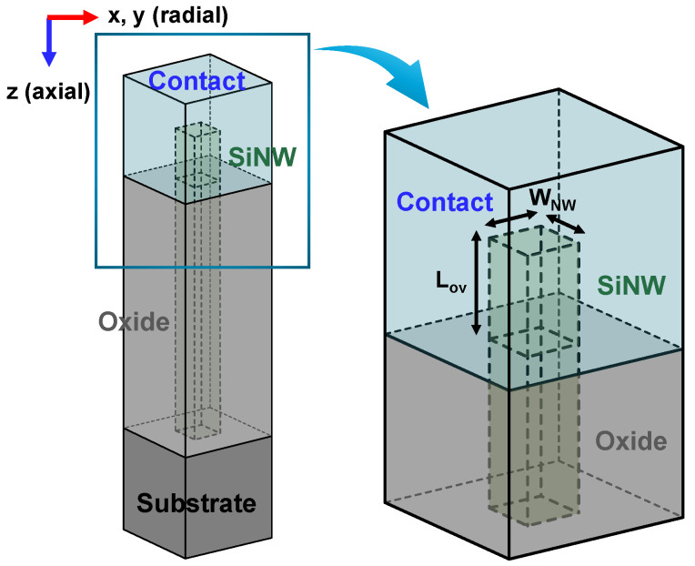 Figure 1
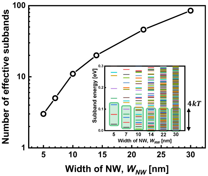 Figure 2
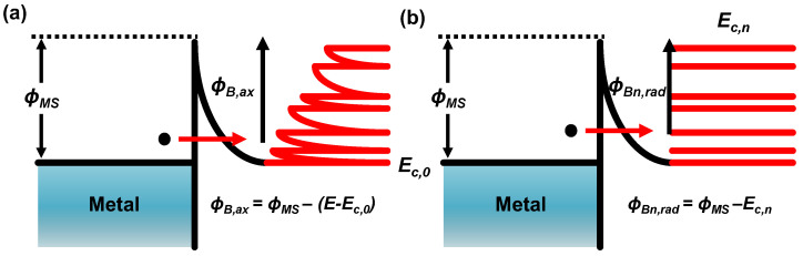 Figure 3
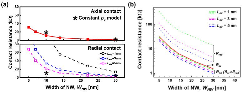 Figure 4
- —National R&D Program through the National Research Foundation of Korea (NRF)
Peer Reviews
No public reviews on file for this paper yet. If you reviewed it on a platform where reviews are public (OpenReview, ICLR, NeurIPS, ICML), you can paste yours below so the community can read it here.
Videos
No videos yet. Explain this paper in a talk, walkthrough, or lecture? Add one.
Taxonomy
TopicsAdvancements in Semiconductor Devices and Circuit Design · Nanowire Synthesis and Applications · Semiconductor materials and devices
1. Introduction
The relentless miniaturization of transistors has driven the relentless pursuit of advancements to mitigate short-channel effects (SCEs) and bolster transistor performance. Strain engineering, high-κ/metal gate (HKMG) materials, and three-dimensional fin field-effect transistors (FinFETs) represent some of the key breakthroughs in this ongoing quest [1,2,3]. FinFETs, leveraging SiGe channels and extreme ultraviolet (EUV) lithography, have successfully achieved scaling down to the 5 nm regime. Gate-all-around (GAA) structures, encompassing nanowires and nanosheets, are actively being explored for technology nodes beyond 5 nm due to their superior gate controllability and enhanced current drivability characteristics [4,5,6]. Among these innovations, vertical nanowire FETs (VNWFETs) have emerged as a frontrunner for sub-3 nm technology nodes, owing to their inherent advantages in design flexibility and their ability to achieve high-density integration facilitated by the vertical channel fabrication process [7,8].
However, despite the aforementioned advantages, VNWFETs face unique challenges in contact formation.
Unlike conventional transistors, the vertical fabrication process necessitates the creation of separate contacts on both the bottom and top sides of the device. While the bottom contact analysis can use established methods, the top contact demands a more nuanced approach due to its geometrical complexity. It comprises two distinct interfaces: the circular top surface (axial contact) and the surrounding side surface (radial contact), formed during top-contact metal deposition. Addressing these contact formation challenges is paramount to propel VNWFET technology towards practical applications in next-generation electronic devices.
As the width of the nanowire (NW) shrinks, its characteristics transition towards a quasi-one-dimensional (Quasi-1D) regime. Consequently, investigating contact resistance with due consideration for NW dimensions becomes increasingly important [9,10,11,12]. Prior studies employed compact modeling to analyze parasitic components within structurally asymmetric VNWFETs, specifically focusing on 10–15 nm nanowires [13]. This modeling approach, which utilized a constant contact resistivity parameter, revealed that the top and bottom electrode asymmetry leads to imbalances in parasitic resistance and capacitance, ultimately impacting device performance. However, as NW dimensions approach the sub-10 nm scale, quantum confinement effects come into play. These effects, including bandgap widening and subband splitting, cause the nanowire’s characteristics to deviate significantly from bulk properties, profoundly influencing the contact characteristics at the metal–semiconductor interface [14].
In this study, we used a semi-classical approach that incorporates one-dimensional (1D) quantum effects specific to the top contact structure of VNWFETs. As NW dimensions decrease, the relevant density of states (DOS) exhibits a transition towards Quasi-1D characteristics, distinct from bulk behavior. This phenomenon has a significant impact on the tunneling mechanisms in both the axial and radial directions. By accounting for these quantum confinement effects, we investigated the top contact resistance along both the axial and radial directions. Additionally, we analyzed the influence of overlap distance on the contact resistance. This comprehensive examination aims to shed light on the intricate behavior of VNWFETs, a crucial step towards their continued development and practical implementation in nanoelectronic devices.
2. Modeling of Q1D Transport in Top Contact
Figure 1 shows a schematic diagram of a vertical nanowire (NW) structure where the top contact comprises two interfaces: one covering the top surface, referred to as the axial contact, and the other covering the side surface with an overlap length L_ov_, referred to as the radial contact.
To take into account the quantum confinement effect of the Si nanowire, the quantized energy states of the NWs can be calculated by solving the Schrödinger equation to determine the discrete energy levels, as expressed by [15]:
where ℏ denotes the reduced Planck constant, n represents the quantum number for the confined direction, m^^* is the effective mass of the electron, and W_NW_ represents the width of the square NW. This equation provides insight into the behavior of electrons within the nanowire, crucial for understanding VNWFET characteristics and optimizing device performance for advanced electronic applications.
Figure 2 depicts the relationship between the width of the nanowire (W_NW_) and the number of effective subbands it possesses. These subbands are defined as the quantized energy levels within a specific range, encompassing the lowest subband energy (E_c_,0) and extending up to E_c_,0 + 4kT. The inset of Figure 2 provides a more detailed illustration of these quantized energy levels, calculated using Equation (1) as a function of W_NW_. At room temperature, the Fermi–Dirac probability function (f(E)) indicates that approximately 98% of the electrons populate the subbands that fall within the 4kT energy range. Notably, a crucial observation from Figure 2 is the significant decrease in the number of effective subbands that significantly influence electron transport. This number rapidly diminishes to 10 or fewer subbands when the WNW falls below 10 nm.
Continuing our analysis with reference to the energy band diagram presented in Figure 3, we can examine the mechanism of electron transport within the nanowire for both the axial and radial contacts. In both cases, electron transport occurs through a process known as field-emission tunneling. Under the assumption that the source/drain (S/D) extension regions are sufficiently doped, the metal–nanowire interface is typically modeled as an Ohmic-like Schottky contact. This assumption is based on the nanowire possessing a sufficiently small width and a doping concentration of 1 × 10^20^ cm^−3^. However, a critical distinction between the axial and radial contacts arises due to the influence of a parameter stemming from the inherent Quasi-1D quantum effects.
The density of states (DOS) in the axial direction of the nanowire of each subband energy can be calculated using the following equation [12]:
where E is the energy of the electron, and E_c,n_ are the quantized subband levels. In an NW with a sub-nanometer diameter and significant length, carrier motion is confined to a 1D space. Consequently, carriers traverse a continuous spectrum of energy states along the wire’s axis, while their motion in the radial direction is constrained to specific quantized energy levels. In the axial contact, tunneled electrons encounter a continuum of energy levels, whereas along the radial direction, they encounter discrete energy levels. The tunneling probability was calculated using the Wentzel–Kramers–Brillouin (WKB) approximation method, which is expressed as
where ϵ_s_ is the permittivity of the semiconductor, N_d_ is the doping concentration of the semiconductor, ϕ_B_ is the tunneling barrier height, and V is the bias voltage.
The tunneling thickness was determined by calculating the depletion width of the metal–semiconductor contact using the formula , where Fermi-level pinning effects were disregarded due to the specific charge characteristics of one-dimensional nanowires [16]. The tunneling barrier height (ϕ_B_) for both the axial and radial contacts was obtained using Equations (4) and (5), respectively. As shown in Figure 3, electrons encounter distinct barrier heights depending on their transport directions. Those tunneling through the axial direction face a continuum of energy states, suggesting that the axial barrier height is continuous, given by
Those traversing the radial direction face the quantized barrier heights that depend on the quantized levels:
For the metal contacts, titanium was selected, commonly employed as the initial layer in modern CMOS processes, setting the metal–semiconductor work function difference ( ) to 0.3 eV in this scenario.
3. Calculation of Axial and Radial Contact Resistances
Figure 4a shows the contact resistance of the axial (R_ax_) and radial (R_rad_) contacts, determined from the current density calculated using the following equation:
where q is the electron charge, v is the velocity of the electron, k is the Boltzmann constant, T is the temperature, g(E) is the density of states, f(E) is the Fermi–Dirac distribution probability, and T(E) is the tunneling probability.
In the case of a 30 nm nanowire width (W_NW_), our proposed approach yields results for the axial contact resistance (R_ax_) and radial contact resistance (R_rad_) that are comparable to those obtained using the previously established constant contact resistivity (ρ_c_) model, which uses experimentally determined contact resistivity values [13]. This suggests that for larger-diameter NWs, the ρ_c_ model can provide a reasonable approximation. However, the ρ_c_ model suggests that the radial resistance (R_rad_) can be lowered compared to the axial resistance (R_ax_) by simply adjusting the overlap length (L_ov_). For instance, with an overlap length of 5 nm and W_NW_ of 10 nm, the ρ_c_ model predicts an axial resistance of approximately 20 Ω and a radial resistance of approximately 10 Ω. This implies that the total contact resistance can be primarily attributed to the combined effects of both axial and radial resistances. However, for NW diameters below 15 nm, a significant discrepancy emerges between the two models. As previously mentioned, only quantized energy levels are relevant for electron transport in the radial direction. Consequently, the influence of W_NW_ on radial resistance becomes considerably more pronounced compared to in the axial direction, highlighting the limitations of the ρc model for sub-15 nm NWs. Consequently, even with an augmented L_ov_, R_rad_ consistently maintains higher values than R_ax_.
In Figure 4b, the influence of R_ax_ and R_rad_ on the total resistance of the top contact, R_tot_, is shown. According to our proposed model, due to the quantum confinement effect, R_rad_ consistently exhibits a larger value compared to R_ax_ regardless of L_ov_. Therefore, R_tot_ can be represented as the parallel of R_ax_ and R_rad_, confirming that it is primarily determined by R_ax_.
4. Conclusions
This investigation explores the impact of contact structure on the electrical characteristics of quasi-one-dimensional vertical nanowire field-effect transistors (VNWFETs). These devices feature a distinctive top contact, consisting of two regions: the upper circular area and the circumferential contact encircling the sidewall. Due to the inherent one-dimensional nature of these contact interfaces, they exhibit distinct contact resistance behaviors. The conventional method of calculating contact resistance, based on contact area and specific contact resistivity between the metal and semiconductor, proves inadequate for nanowire contacts with sub-nanometer diameters due to quantum confinement effects. In Quasi-1D VNWFETs, electrons traveling in the radially confined direction encounter strictly quantized energy levels, greatly limiting their tunneling probability compared to the continuous energy states available along the axial direction. Consequently, as nanowire dimensions decrease, electron tunneling in the radial direction experiences a significant reduction in current compared to tunneling along the axial direction. This critical observation underscores the necessity of considering both distinct interface types for effective device performance optimization. Our findings emphasize the crucial need for accurate modeling of quantum confinement effects, particularly in VNWFETs approaching or falling below the 10 nm threshold.
The reference list from the paper itself. Each links out to its DOI / PubMed record.
- 1Chidambaram P.R. Bowen C. Chakravarthi S. Machala C. Wise R. Fundamentals of silicon material properties for successful exploitation of strain engineering in modern CMOS manufacturing IEEE Trans. Electron Devices 20065394496310.1109/TED.2006.872912 · doi ↗
- 2Wu C.C. Lin D.W. Keshavarzi A. Huang C.H. Chan C.T. Tseng C.H. Chen C.L. Hsieh C.Y. Wong K.Y. Cheng M.L. High performance 22/20nm Fin FET CMOS devices with advanced high-k/metal gate scheme Proceedings of the 2010 IEEE International Electron Devices Meeting (IEDM)San Francisco, CA, USA 6–8 December 2010
- 3Tang S.H. Chang L. Lindert N. Choi Y.-K. Lee W.-C. Huang X. Subramanian V. Bokor J. King T.-J. Hu C. Fin FET-a quasiplanar double-gate MOSFET Proceedings of the 2001 IEEE International Solid-State Circuits Conference San Francisco, CA, USA 7 February 2001
- 4Bangsaruntip S. Cohen G.M. Majumdar A. Zhang Y. Engelmann S.U. Fuller N.C.M. Gignac L.M. Mittal S. Newbury J.S. Guillorn M. High performance and highly uniform gate-all-around silicon nanowire MOSFE Ts with wire size dependent scaling Proceedings of the 2009 IEEE International Electron Devices Meeting (IEDM)Baltimore, MD, USA 7–9 December 2009
- 5Lauer I. Loubet N. Kim S.D. Ott J.A. Mignot S. Venigalla R. Yamashita T. Standaert T. Faltermeier J. Basker V. Si nanowire CMOS fabricated with minimal deviation from RMG Fin FET technology showing record performance Proceedings of the 2015 Symposium on VLSI Technology Kyoto, Japan 16–18 June 2015
- 6Mertens H. Ritzenthaler R. Chasin A. Schram T. Kunnen E. Hikavyy A. Ragnarsson L.-Å. Dekkers H. Hopf T. Wostyn K. Vertically stacked gate-all-around Si nanowire CMOS transistors with dual work function metal gates Proceedings of the 2016 IEEE International Electron Devices Meeting (IEDM)San Francisco, CA, USA 3–7 December 2016
- 7Guerfi Y. Larrieu G. Vertical silicon nanowire field effect transistors with nanoscale gate-all-around Nanoscale Res. Lett.20161121010.1186/s 11671-016-1396-727094824 PMC 4837198 · doi ↗ · pubmed ↗
- 8Veloso A. Altamirano-Sánchez E. Brus S. Chan B.T. Cupak M. Dehan M. Delvaux C. Devriendt K. Eneman G. Ercken M. Vertical nanowire FET integration and device aspects ECS Trans.201672314210.1149/07204.0031 ecst · doi ↗