An Extended Kolmogorov–Avrami–Ishibashi (EKAI) Model to Simulate Dynamic Characteristics of Polycrystalline-Ferroelectric-Gate Field-Effect Transistors
Shigeki Sakai, Mitsue Takahashi

TL;DR
This paper introduces a physics-based model to simulate polarization switching in ferroelectric polycrystalline films used in FeFETs, aligning well with experimental results.
Contribution
The paper proposes an extended Kolmogorov–Avrami–Ishibashi (EKAI) model for dynamic polarization switching in polycrystalline ferroelectric films.
Findings
The EKAI model accurately describes polarization domain nucleation and wall propagation under time-dependent electric fields.
Switching time scales follow an exponential dependence on the electric field and grain orientation angle θ.
The model explains the broad switching time distribution observed in FeFETs without assuming non-physical functions.
Abstract
A physics-based model on polarization switching in ferroelectric polycrystalline films is proposed. The calculation results by the model agree well with experimental results regarding dynamic operations of ferroelectric-gate field-effect transistors (FeFETs). In the model, an angle θ for each grain in the ferroelectric polycrystal is defined, where θ is the angle between the spontaneous polarization and the film normal direction. Under a constant electric field for a single-crystal film with θ = 0, phenomena regarding polarization domain nucleation and wall propagation are well described by the Kolmogorov–Avrami–Ishibashi theory. Since the electric fields are time-dependent in FeFET operations and the θ values are distributed in the polycrystalline film, the model in this paper forms an extended Kolmogorov–Avrami–Ishibashi (EKAI) model. Under a low electric field, the nucleation and…
Genes, proteins, chemicals, diseases, species, mutations and cell lines named across the full text — each resolved to its canonical identifier and authoritative record.
Click any figure to enlarge with its caption.
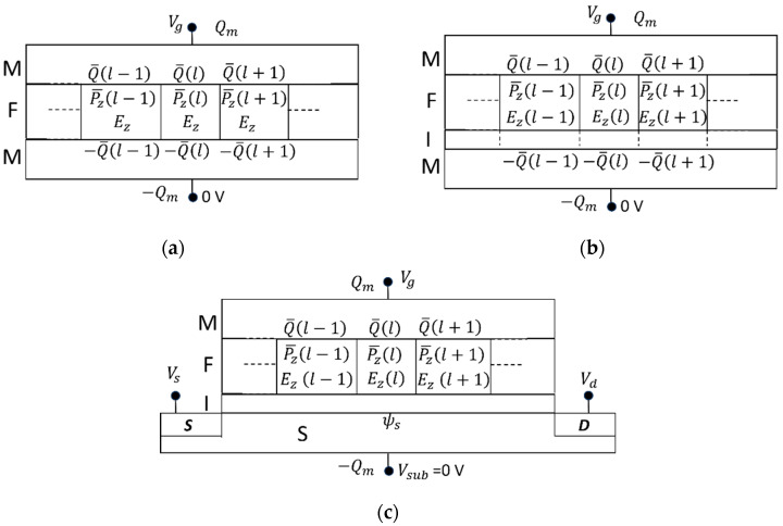 Figure 4
Peer Reviews
No public reviews on file for this paper yet. If you reviewed it on a platform where reviews are public (OpenReview, ICLR, NeurIPS, ICML), you can paste yours below so the community can read it here.
Videos
No videos yet. Explain this paper in a talk, walkthrough, or lecture? Add one.
Taxonomy
TopicsFerroelectric and Piezoelectric Materials · Ferroelectric and Negative Capacitance Devices · Multiferroics and related materials
1. Introduction
1.1. Necessity of a Physics-Based Model for Ferroelectric Device Dynamics
Ferroelectric-gate field-effect transistors (FeFETs) have attracted attention not only because of their potential functionality [1,2] such as being compact, non-volatile, and non-destructive-read memory cells, but also due to recent rich accumulations of experimental data. FeFETs have been characterized by various measurements. Quasi-static characteristics of drain current ( ) vs. gate voltage ( ) are measured with slow sweeping by a semiconductor parameter analyzer. Also, vs. are measured by a quasi-static procedure with the slow sweeping by a ferroelectric tester. The is the metal-gate charge density induced by ferroelectric layer polarization. Dynamic time-dependent properties of FeFETs are characterized by a pulse-write-and- -read (PWVR; see Figure A3) or pulse-write-and- -read (PWIR) method. The pulse-write (PW) is done by a pulse generator. In a FeFET, while a positive or negative pulse is given with the height of (>0) or (<0), ferroelectric polarization responds dynamically as a function of pulse height ( or ) and time width ( ). After ceasing PW, considerable amounts of ferroelectric polarization are retained due to ferroelectricity. This retained polarization is a function of , , and . A read operation is done after PW, where of the transistor is swept in a narrow voltage range slowly compared to the PW time scale. A threshold voltage ( ) is read for PWVR, and the drain current ( ) is read at a fixed for PWIR. A threshold voltage difference (Δ ) for PWVR or a current ratio between the high- and low- -current states for PWIR can be derived for a pair of the write voltages; and . Δ by PWVR or the ratio by PWIR is a performance indicator of an FeFET as a nonvolatile memory transistor.
A lot of experimental results by PWVR and PWIR are available to investigate dynamic polarization switching in metal ferroelectric insulator-semiconductor (MFIS) type FeFETs, whose ferroelectric is SrBi_2_Ta_2_O_9_ or (Sr_1−x_Ca_x_)Bi_2_Ta_2_O_9_ [3,4,5]. The former and the latter are abbreviated as SBT and CSBT, respectively. The SBT and CSBT belong to a family of the Bi-layered perovskite oxides with similar electrical properties. The coercive field of CSBT for x = 0.1–0.2 is 10% larger than that of SBT. Hereafter, FeFETs comprising SBT or CSBT in the ferroelectric layers are called SBT-FeFETs. The electric properties of SBT-FeFETs are suitable for model verification because they are reproducible with high switching endurance due to negligibly small charge injection and trapping in the FeFET gate stacks.
Despite the many experimental works of PWVR and PWIR reported in detail, there have been no correct theories based on physics for simulating them. As one of the existing models, a phenomenological Landau–Ginzburg–Devonshire (LGD) theory in ferroelectrics constructs a Gibbs free energy for the ferroelectrics where the primary energy term is expressed as a polynomial expansion form of polarization as an order parameter [6,7,8]. By minimizing the free energy, equilibrium or quasi-static properties are derived. The LGD theory described the transition between the paraelectric and ferroelectric phases with temperature variation across the Curie temperature [7]. It also described phase transitions between the tetragonal and orthorhombic and between the orthorhombic and rhombohedral in BaTiO_3_, a cubic-based ferroelectric material [6]. In the Gibbs free energy, the spatial differentiation term brought non-homogeneity, by which domain patterns were described [9,10]. The Gibbs energy for ferroelectrics can include the elastic energy term and the coupling terms of elasticity and polarization since the polarization accompanies lattice displacement of crystals. In the case that the ferroelectric layers are divided into LGD segments, the LGD theories are called phase field models [11,12]. The models showed coexistence of 180°- and non-180° domains under constraints of substrates [11] and polycrystalline grain growth [13].
The LGD theory has its own representation of time dependence. In the case that the electric properties without elastic terms are matters of concern, the description of time dependence is sometimes called the Laudau–Khalatnikov (LK) equation [14,15,16]. In the phase-field models, it is called the time-dependent Ginzburg–Landau (TDGL) equation [11,17]. LK and TDGL are essentially the same. A Lagrangian function, which includes a simple viscosity term of classical mechanics [18], may help us comprehensively understand the origin of the time-dependent polarization switching. The Gibbs free energy for the ferroelectrics replaces the potential term in the Lagrangian. In deriving equations of motion, the inertia term is usually neglected for polarization reversal problems, and the LK and TDGL equations are obtained [19]. Overdamped (i.e., strong viscosity) cases in the Lagrangian may allow us to omit the inertia term in the equation of motion. As is obvious from the derivation of these time-dependent equations, however, the LK and TDGL equations are deterministic and do not have thermal activation forms in them. As indicated by previous papers [20,21,22], nucleation and domain-wall propagation under an electric field occur via thermally activated steps. Thus, the LK and TDGL equations are not suitable (at least quantitatively). Additions of Gaussian white-noise terms to these equations are necessary for describing the thermal activation steps, and in fact the effect of the noise term was demonstrated for a small segment number case [23]. However, since the LDG segments should be finer than the domain-wall width and the wall width size is one crystal lattice or a few times of it [24,25], the number of the LDG segments for general objects including polycrystalline films becomes so huge that we cannot make calculations within a realistic time scale.
This paper proposes a physical model for describing polarization variation with time in a ferroelectric film and for calculating electronic device operations of FeFETs, metal-ferroelectric-metal (MFM) capacitors, and metal-ferroelectric-insulator-metal (MFIM) capacitors. In the model, the ferroelectric film can be a polycrystalline one, and to each grain, an angle is assigned where is the angle between the film normal and the direction along the spontaneous polarization. The distribution in the polycrystalline film is given by experiments. In fact, for SBT-based FeFETs, the angle distribution was derived by an electron backscattering diffraction (EBSD) patterns technique [26].
In each grain having , it is also assumed that, under an electric field, a seed for polarization reversal grows along the spontaneous direction and forms a narrow columnar 180° reversed domain, which is expanded along the sidewise direction, because 180° switching and ±180° domain formation are subjected to occur in SBT and CSBT ferroelectrics [27,28,29]. Experimental observations of the 180° switching and 180° domain-wall moving for ≠ 0 cases are found in [30,31].
The Kolmogorov–Avrami–Ishibashi (KAI) model [32,33,34,35,36] fits the physical picture mentioned above (i.e., 180° domain nucleation and domain wall propagation). The KAI model provides mathematical functions of the = 0 case describing domain expansion with time under a constant electric field. As for epitaxial thin films, many papers indicated good agreement of the KAI model with experiments [37,38], but for polycrystalline films, the KAI model is asserted to be unsuitable [39]. This complicated issue concerning polycrystal films will be overcome in our present paper by introducing terms in grains. In order to explain wide-range log ( ) distributions of polarization switching times that Pt/Pb(Zr,Ti)O_3_/Pt capacitors showed, the inhomogeneous field mechanism (IFM) model [40] and the nucleation-limited switching (NSL) model [41] are proposed. Although switching reversal experiments in polycrystalline films were explained [42,43] using the IFM, the model assumed inhomogeneous electric-field distribution of a Gaussian type, which was not physics based. The NLS is a non-KAI model. A (111)-oriented Pb(Zr,Ti)O_3_ was used. The waiting times of elementary regions are stochastic. By giving an exponentially broad distribution of the waiting time, the switching phenomena across a wide log ( ) scale were described. Since the distribution function is assumed so that the numerical results reproduce the experimental ones, understanding the physics of the distribution function is not easy. If we infer a possible inclusion of grains with other crystal orientation in the film, physics in the wide log ( ) characteristics might be explained by an effect of the orientation distribution. A HfO_2_-based FeFET is reported to be consistent with the NLS [44]. The paper indicates that the grain size is ≈20 nm and the field for creating a nucleus is ≈1 MV/cm. This suggests that the nucleation size is already the same as the grain size, and thus there is no space left for the created nucleus to induce a wall expansion supposed in the KAI model.
Herein we propose an extended KAI (EKAI) model, which is applicable to represent characteristics of FeFETs with polycrystalline ferroelectrics under time-dependent electric fields. In the EKAI model, KAI-like pictures are adopted only inside individual grains. The EKAI describes 180° switching and ±180° domain wall propagations in every grain separately. No wall motions are assumed to propagate across adjacent grains. There are two fundamental premises of the EKAI. One is that only the electric field component along the spontaneous polarization works for the polarization switching. The other is that we pick up only the film-normal component of the switched polarization because the film-normal component is the important response to the externally applied potential. The in-plane components of the switching polarization are expected to be randomly distributed among grains. The effect of the in-plane components is thought to be weak because of the random distribution, and thus the boundary conditions between neighboring grains are ignored in the present EKAI model. The polarization of the KAI model is an averaged quantity where the polarization is represented by the average of the volume fraction of ±180° domain regions. The EKAI has a distinct perspective on ferroelectrics from the phase-field model in which the ferroelectrics are divided into small segments connected by strict boundary conditions according to the idea of the LGD. The EKAI has a much shorter computation time than the phase-field model because it ignores the grain boundary conditions and averages the ferroelectric polarizations in grains. The PWVR and PWIR data show a wide time range of polarization switching characteristics from 50 ns to 10 ms [3,4,5]. We suppose that these rather slow and wide-ranged time responses are attributed to ferroelectric polycrystals consisting of grains that have broad distributions in the crystal orientations. The response times of the paraelectric components in the ferroelectric grains and the dielectrics in the insulator are supposed to be much shorter than those of the polarization-switching components. The potential formation time in the semiconductor is also supposed to be shorter. Therefore, the EKAI model in this paper assumes that the parameters except for the polarization switching in the ferroelectric grains vary instantaneously. Correctness of the EKAI model is supported by good agreement with experimental results of quasi-static – , – , and PWVR for SBT-based FeFETs as discussed later in Section 4. The EKAI model in this paper assumes no free charges existing in the gate insulator and ferroelectric; thus the EKAI is not directly applicable to HfO_2_-based FeFETs in which the ferroelectric polarization switching is always accompanied by charge injection currents [45,46,47,48,49].
1.2. Presentation of the KAI with the Characteristic Times for the EKAI Model
Let us write some equations of the original KAI model, because they are necessary in the succeeding section for the EKAI derivation. In the original KAI, polarization switching nucleation is instantaneous in comparison with domain growth motion. A constant electric field and the domain wall velocity ( ) depending on this constant field are assumed. As shown in Figure 1, the ferroelectric volume is constituted by domain regions. The switching polarizations in the downward and upward regions are and , respectively. is the spontaneous polarization. The polarization direction is parallel to the z-axis. The downward (or upward) domain regions expand with time under a positive (or negative) field, after application of step function with a constant positive field, . Consider a case that at the initial (t < 0) the volume is occupied fully by the upward regions, and a step function with a constant positive field, is applied at = 0. Then, the volume fraction of the downward domain ( ) is varied with time for ≥ 0 under a constant as
with
is the characteristic time for the polarization switching and is a function of the constant field . The power exponent, , is a parameter relating to the domain growth dimension. The volume fraction of the upward domain ( ) is
The switching polarization ( ) averaged over the ferroelectric volume is
Similarly, in the case that at the initial (t < 0) the volume is occupied fully by the downward regions, and step function with a constant negative field, is applied at = 0, the volume fraction of the upward domain ( ) is for t ≥ 0 under a constant :
in Equation (2) is a function of the constant field . The switching polarization ( ) averaged over the ferroelectric volume is
According to Ishibashi and Takagi [36] and Ishibashi [50], in category 1, domain nucleation occurs with a fixed probability, and = 3 when the wall shape is two-dimensional (i.e., circular) and = 2 when the wall shape is one-dimensional (i.e., straight line). In category 2, there exist latent nuclei, and no new nucleation appears. In category 2, = 2 when the shape is two-dimensional, and = 1 when it is one-dimensional. In real materials, domain nucleation may occur, and latent nuclei may also exist. Some parts are two-dimension and others are one-dimensional-like. Hence the value is not an integer of the range 1 ≤ ≤ 3. When is small in Equation (2), the transient time of the polarization reversal is short, and when is large, it is long. That is, is a characteristic time that gives a time scale of the polarization variation. has a relationship with .
For category 1,
For category 2,
In Equation (7), and are constants.
The KAI model did not show explicit mathematical forms of . The wall velocity as a function of the applied film-normal electric field ( ) has been investigated mainly by switching current measurement of single crystals [51,52] and by piezoresponse force microscopy (PFM) of epitaxial thin films including random disorder by defects [21,53,54]. A consensus view in the case of films including the disorder is that under high electric fields quickly increases in linear equation whereas it creeps up in reciprocal exponential at low fields [52,55]. In the case of ferroelectric films including defects, under high field is expressed as for ≫ , where is a critical field over which depinning of wall motions occurs at 0 K [55,56]. In an intermediate region, is expressed using a power exponent as
and in a low- creep region, is expressed at finite temperature as
where is a scale of energy barrier and σ is a power exponent originated from random disorder defects in ferroelectric films [55,56] ( : the Boltzmann constant and : the absolute temperature).
From Equations (7) and (8), the expressions are changed to expressions. Using a renormalized constant , Equation (8a) is, irrespective of the category 1 or 2,
Similarly, irrespective of the categories, Equation (8b) is converted to , using a renormalized constant U, as
where is a constant.
In the present work, experimental results of SBT-based FeFETs are used in order to demonstrate the EKAI model’s credibility. High endurance of the SBT FeFETs can be realized on small or at least moderate write-voltage conditions where the charge injection and trapping in the gate stack are suppressed [2,57]. Since a small or moderate write voltage brings a low electric field in the ferroelectric, we adopt Equation (9b) rather than Equation (9a) hereafter in this paper; i.e., Equation (9b) will be used in calculations shown later. Further, since the separate determination of and is difficult, we have the following equation for in this paper:
with an activation field constant . To include negative cases, instead of , is used in Equation (10).
2. EKAI Model
Let us consider a ferroelectric polycrystal film as shown in Figure 2a. The thickness of the film is The film is divided into plural grains labeled from one to . All grains have the common thickness Grain boundaries are along the film normal, i.e., the z-axis. The area of grain is . The direction of the spontaneous polarization of grain is parallel to the axis. The angle between the axis and the z-axis is . The range of is defined as . All grains have a same spontaneous polarization, or . The polarization of the direction of the axis is defined as .
In Section 4, the EKAI model will be compared to the experimental results of MFIS FeFETs, where the ferroelectric layers consist of ferroelectric polycrystals. Experimental FeFETs with 135 nm thick ferroelectric SBT layers are available for discussion in the present EKAI model. Averaged in-plane diameters of the SBT grains are about 200 nm, which is larger than the ferroelectric layer thickness in the FeFETs. Therefore, we shall assume a single grain occupation along the z-direction or the film normal in the SBT FeFETs. Each grain stands as a pillar with a constant cross-section from the film top to the bottom.
Figure 2b is an expanded schematic picture of grain . The grain consists of upward domain regions and downward domain regions. In the downward (or upward) domain regions, the spontaneous polarization (or ) is parallel (or anti-parallel) to the axis. Figure 2c is a schematic picture focusing on a cylindrical-shape downward domain existing in the grain. The EKAI model in this section describes polarization variation in one grain. In the model, there are two fundamental assumptions (described in Section 2.1 and Section 2.2) prior to the significant description (Section 2.3) of the polarization dynamics under a varying electric field with time. Section 3 provides calculation schemes for the following specific devices including ferroelectric polycrystal: (1) MFM capacitors, (2) MFIM capacitors, and (3) MFIS FeFETs.
2.1. Polarization Variation under a Constant Electric Field
In grain , the polarization direction is tilted from the z-axis by . Nevertheless, it is assumed that, under a constant field, , the wall-motion equations are formally the same as Equations (1)–(6) of the KAI model.
Consider a case that a positive constant field as a step function is applied at . At t < 0, the volume is occupied fully by the upward regions. Then, the volume fraction of the downward domain ( ) is varied with time for as
The volume fraction of the upward domain ( is
The switching polarization ( ) averaged over the volume of grain is
Consider the opposite case that a negative constant field as a step function is applied at . At t < 0, the volume is occupied fully by the downward regions. Then, the volume fraction of the upward domain ( ) is varied with time for as
The switching polarization ( ) averaged over the volume of grain is
2.2. Effect of the Spontaneous Polarization Direction Different from the Z-Axis
The function in Equations (11)–(15) is , which is the same as Equation (2). However, the axis is tilted from the z-axis by . In the EKAI model, the characteristic time for the polarization switching is assumed to be
i.e., replaces in Equation (10).
2.3. Switching Polarization under Time-Dependent Electric Fields
Let us consider switching polarization evolution in grain in the case that the electric field varies with time. Using the information of , , and , and are derived by the method of this subsection, where ( : a small time-increment), and or means the amounts of at or , respectively.
The EKAI model assumes that the polarization varies during a short period as if the polarization varies under a constant field . Note, however, that we must consider two cases, i.e., the cases of and .
Figure 3 shows an explanation for the case . Let us consider a case in grain that, at , is under = . This status is point A in the graph. Draw a curve of the EKAI function (Equation (11)) at a constant field, = , as the blue solid line . Note that always starts from the origin of the graph (i.e., at Time = 0.) The line has at point B. The time at point B is , which is obtained by solving the (Equation (2)) as
with
We assume that the growth of from to = under = at point A is the same as the growth of at point B under the same constant field . The distance between points A and B is . The growth during at the point A can thus be calculated by a parallel-shifted function, , and thus in the case of is obtained as
The volume fraction of the upward domain and the z-axis component of the switching polarization averaged over grain are
and
Quite similarly, we derive the following equations in the case of . The volume fractions of the upward domains and the downward domains are
and
with
The z-axis component of the switching polarization averaged over grain is
The electric field can be obtained using the obtained (Equation (21) or Equation (25)) and the electrostatic equation, which depends on the device structure considered. See the next section. Once is obtained, we know now , , and . Then, the quantities of are regarded as the quantities at of ; we can repeat calculation.
When is infinitesimally small, Equations (19) and (22) can be expressed as a differential style of and , that is, for ,
and for ,
The physical meaning of Equations (26) and (27) is that the differential of at point A in Figure 3 equals the differential of at point B.
3. Total Calculation Scheme for Describing Time-Varying Switching Polarizations of Specific Devices
Figure 4 shows a schematic drawing of (a) an MFM capacitor, (b) an MFIM capacitor, and (c) an MFIS FeFET. As stated before, the ferroelectric film consists of poly-crystal grains indexed by with . We apply a time-dependent voltage, , to the top metal electrode of the MFM and MFIM capacitors and to the gate metal electrode of the MFIS FeFET. We provide the ground voltage, 0 V, to the bottom metal electrode of the MFM and MFIM capacitors and to the semiconductor substrate terminal.
Following the EKAI model in the previous section, we derived, at a moment, the z-axis component of the switching polarization averaged in the volume of grain .
We assume that the paraelectric component of the ferroelectric is isotropic. The electric displacement averaged in the volume of grain is represented as
where is the permittivity in vacuum and is the dielectric constant of the paraelectric component of the ferroelectric.
Total calculation scheme for specific devices. (a) an MFM capacitor; (b) an MFIM capacitor; (c) an MFIS FeFET. The EKAI model under a varying field Ez with time provides Pz¯l, Rdnl, and Rupl at t=tnext using Rdnl, Rupl, and Ezl at t=tnow. To repeat the calculation, it is necessary to obtain Ezl at t=tnext. Depending on the structure of the specific devices, the method of deriving Ezl is different. For an MFM capacitor case (a), Ezl does not depend on l, and Ez at t=tnext is obtained by Equation (33). For an MFIM capacitor case (b), the induced charges of the bottom electrode of grain l, −Q¯l is a good approximation. Ezl depends on l. Ql at t=tnext and is derived by Equation (38). Then Ezl at t=tnext is obtained by Equation (37). For an MFIS FeFET case (c), Dz at the top surface of the insulator is averaged over all the grains due to a transitional thin layer between the ferroelectric and the insulator (see Figure 5). The surface potential ψs of the semiconductor is assumed to be uniform because of insufficient acceptor density NA. The uniform Dz and ψs lead to a grain-independent field Ez [Ezl=Ez for all l]. ψs at t=tnext is derived by Equation (42). Then, Qm is obtained from Equation (44), and Ez is obtained from Equation (40).
The metal electrodes of all the three devices are assumed to have large free carrier densities. At the metal electrode surfaces facing the ferroelectric or insulator, the electric-field penetrations are negligibly small, and thus no potential variations inside the metal can be assumed. The potential in the metal is uniformly . Following Equation (28) and Gauss’s law, the induced charge per unit area facing the grain is
Because of the averaged value of , is also averaged in the volume of grain . The total induced charges of the top metal electrode of the potential, , is the summation of the induced charge over all the grains. The total induced charges are defined as the charge per unit area, , which is
where is the area that grain faces the electrode and . This is the quantities obtained experimentally in measurements, which are explained in (2) in Appendix A. The switching polarization (i.e., not including the paraelectric polarization) averaged over the entire ferroelectric, , is as
Using the EKAI and electrostatic equations across MFM, MFIM, and MFIS stacks, calculation steps are expressed as follows.
3.1. MFM Capacitor
The electrostatic equation of the MFM capacitor is
where is the voltage across the ferroelectric layer. The flat band voltage, , is the work function difference between the metal top electrode and the metal bottom electrode. Since does not depend on the grains, the electric field is also independent of as
We have Equation (30) as
The second term of Equation (34) is the switching polarization averaged over the entire ferroelectric, (Equation (31)).
Equations (21) and (25) of the EKAI model in the proceeding section can give us the (for ) at . We also know at , because is externally applied. Then, and at are obtained by Equation (33) and Equation (34), respectively. We know the behavior of the MFM capacitor at .
, , and at are regarded as those at . The EKAI model provides and , and at . Equation (33) gives us at . We repeat these procedures and obtain fully the time-dependent solution of the MFM capacitor.
3.2. MFIM Capacitor
Charges appear at the top surface of the bottom electrode. We shall extend the z-axis-orientated boundaries between the adjacent grains into the insulator. We have the potential and relationships for each grain; i.e., we have the following for
and
Here, is the voltage across the grain . is the voltage across the region in the insulator belonging to grain . At the top surface of the bottom electrode corresponding to grain , the induced charge is , and we have for :
with the insulator capacitance, :
and
We eliminate from Equations (35)–(37). Then, we derive
with is the paraelectric component capacitance of the ferroelectric as
The EKAI model provides and , and at . We also know at , because is externally applied. Equation (38) leads to at for all , and Equation (37) gives us at , using the obtained for all . All physical quantities are derived at . Then, similarly to the case of the MFM capacitor, we can return the EKAI model calculation, and consequently we derive the time-dependent numerical solution for the MFIM capacitor.
3.3. MFIS FET
Figure 6 summarizes the total calculation scheme for MFIS FeFETs. Regarding the semiconductor, in the MFIS stack, the acceptor concentration ( ) and carrier density in the semiconductor are much smaller than the carrier density in the metal layer. Thus, the electric field penetration into the semiconductor inevitably occurs so that the semiconductor surface potential is different from the substrate potential ( ). Imagine further a surface case where a region of an inversion state adjoins a region of an accumulation state. The surface potential cannot change abruptly on the surface. A good measure of the potential variation on the surface is the maximum depletion width, , where is the relative permittivity of the semiconductor, the intrinsic carrier concentration, , and the elementary charge [56]. For example, nm when cm^−3^ K using and = 1.45 × 10^10^ cm^−3^ for Si. If the size of ferroelectric grains is smaller than , a uniform surface potential over all the grains is a good approximation (Figure 4c). Figure 5 shows a schematic drawing of a ferroelectric-insulator-semiconductor (FIS) as part of the experimental MFIS FeFETs. As shown in Appendix A, the gate stack of the experimental FeFETs is Ir/CSBT/HfO_2_/Si. Via the crystallization annealing of the CSBT, a 2.6 nm thick SiO_2_ interfacial layer (IL) was formed between HfO_2_ and Si. The HfO_2_ and CSBT layers are 4 nm thick and 135 nm thick, respectively. The bilayer of the HfO_2_ and IL forms the insulator in the MFIS. Transmission electron microscope photos confirmed a thin (about 5 nm thick) transitional layer as shown in Figure 5a [58]. The transitional layer is constituted by fine grains (≈5 nm) whose main elements are originated from the ferroelectric CSBT. Due to the fine sizes, these grains may be non-ferroelectric but work as a high permittivity material. The dielectric constants of this transitional layer, the HfO_2_ layer, and the SiO_2_ IL are typically 180, 25, and 3.9, respectively. The different values of (Equation (28)) at the bottom of the ferroelectric among the grains are averaged via the in-plane pass in the transitional layer (Figure 5b). Therefore, the switching polarization at the interface between the CSBT and the insulator consisting of the bilayer of HfO_2_ and IL can be reasonably assumed to equal the z-axis component of the polarization averaged over all the grains, , that is already defined in Equation (31). Since at the top surface of the insulator and at the bottom of it are uniform laterally, the electric field along the z-axis in the insulator and the potential across the insulator are also laterally uniform, which leads to a grain-independent field [ for all ] in the ferroelectric and a grain-independent potential across the ferroelectric. The z-axis component of the electric displacement averaged over all the grains as well as from Equations (28)–(30) is
FeFETs have the gate, source, drain, and substrate terminals. Let us consider the case where the gate voltage V_g_ is generally varied with time and other terminals are grounded ( ). Here , , and are the voltages applied on the source, drain, and substrate, respectively. The electrostatic equation across the MFIS stack is
where is the flat-band voltage, i.e., the difference between the metal work function and semiconductor fermi level. By eliminating from Equations (40) and (41) and using Gauss’s law while noticing the capacitance definition of Equations (36b) and (39), we have
If there is no interface state density between the insulator and semiconductor, the induced charge density, , in the semiconductor surface region has the same magnitude as with the opposite polarity ( ). is a function of semiconductor surface potential as follows [59]:
with a negative sign for . This equation is for n-channel FeFETs formed in p-type substrates. The equation for p-channel FeFETs can be rewritten appropriately. The Debye length is with and . The donor, acceptor, and intrinsic carrier densities in the semiconductor are , , and , respectively, and and are the equilibrium densities of holes and electrons, respectively.
In the case that the interface states between the semiconductor and insulator are considered, the equation is modified as
where is the trapped charge at the interface per area that is expressed as
Here, is an electron-energy variable, is the area density of interface-states per electron energy, and is the Fermi–Dirac distribution function for acceptors [59].
In the case that is approximated as a constant [V^−1^cm^−2^] with respect to the energy, can be approximated as
For convenience of numerical root-finding calculations, we emphasize that (Equation (43)) monotonically decreases with the increase of , and (Equation (45) or Equation (46)) also has the same monotonical property. Equation (44) shows that is a monotonically increasing function of .
See Equation (42). The right-hand side quantity is a monotonically increasing function of . At in the previous section, we derived for all by either Equation (21) or Equation (25). at is given by an external voltage source. Thus, the left-hand side of Equation (42) is a known constant at . The right-hand side of Equation (42) consists of only one variable and is a monotonically increasing function of . Hence, can be uniquely determined at . Once is determined, we derive from Equations (43)–(46), and from Equation (40) at .
We now have at , and, in the previous section, we have and at for all . The set of , , and at replaces a set of , , and at . If and at are obtained by Equations (19) and (20). If and at are obtained by Equations (22) and (23). The procedure of this section gives us at . Repeating these procedures provides the dynamics of the MFIS FeFETs.
The status of the polarization in ferroelectric or the electric displacement can be monitored by the drain current, , of the sub-threshold region, which is represented as functions of the drain voltage and the surface potential by [59]:
In this paper, all numerical results of FeFETs are obtained on the premise of , whereas the practical measurements of n-channel FeFETs are usually on the condition of and . Such a small difference in condition does not affect the validity of comparing results from the calculations and the measurements.
The EKAI, the formulae from Equations (11)–(27), and the total calculation scheme for MFIS FeFETs, those from Equations (28)–(31) and from Equations (40)–(47), describe the general transient response of MFIS FeFETs under time-dependent conditions. The formulae also cover slowly changing phenomena. There is a so-called data retention mode, in which all the quantities such as , , , and vary very slowly, and the values in Equations (19) and (22) can be chosen flexibly with minimal changes of those quantities; thus, retention results of the period of days and years are obtained in a practical computation time.
4. Calculation Results of FeFETs and Comparison to the Experimental
4.1. Parameters Being Able to Be Assigned
The EKAI model and the total calculation scheme of this paper are verified using experimental data of FeFETs consisting of MFIS gate stacks of Ir/CSBT/HfO_2_/IL/Si. The experimental details are reviewed in Appendix A. An insulator in the modeled MFIS FeFET corresponds to the bilayer of IL and HfO_2_ in a real CSBT FeFET. Capacitance of the insulator ( ) was evaluated as = 0.99 μF/cm^2^. Regarding the ferroelectric, the dielectric constant of the paraelectric component is determined by the curves at < 0 or in the third quadrant of Figure A2 because the semiconductor depletion layer does not affect at < 0. In the third quadrant, by taking the gradient of the curve of a V_g_ sweep amplitude, the combined capacitance of and (Equations (36b) and (39)) was 0.54 μF/cm^2^. Since = 0.99 μF/cm^2^ and = 135 nm, = 180 at room temperature was obtained and used for calculation in the EKAI. The direction of SBT and CSBT ferroelectrics is the a-axis direction of the crystal unit cell of SBT and CSBT [60,61].
With regard to the angle and the area , the technique of EBSD patterns could characterize the crystal orientation and grain size. The bar graph plots in Figure 7 show the distribution function of grains with the orientation angle . The quantity of the vertical axis is the area of grains whose is in the range from to ( : the bar width). The scanning area of EBSD, ≈ 56 μm^2^, is not enough for statistical treatment, meaning that versus curves simulated by the EKAI model and the calculation scheme using the bare bar graph plots were not smooth. As shown in Figure A4, the experimental curves are very smooth. Therefore, we used a fitted smooth curve in Figure 7 instead of the bare data. Although the smoothed curve is used in the actual calculation, the curve is digitized at every 3° to save calculation time.
When we make quasi-static calculation of and , a sinusoidal function is provided as . The frequency and the calculation time length are typically set as 10 Hz and 0.2 s, respectively. The time step = 1 × 10^−9^ s is commonly used in the calculation of , , and PWVR. Validity of the value and accuracy of the calculated results were verified by confirming that calculations with = 0.5 × 10^−9^ s gave the same results as those with = 1 × 10^−9^ s.
Experimental curves do not suggest any electron-energy dependence of in Equation (45), and thus we use and Equation (46) regarding the interface states between the insulator and semiconductor. Several series of simulations with various and values were examined and compared to the experimentally obtained . We found that = 4 × 10^12^ V^−1^cm^−2^ is a good value to fit the experiment. Regarding , the suitable range was between −0.8 V and −1.0 V, and thus we used = −0.8 V in this work.
According to the PFM experiments and the analyses by phenomenological theories including random disorder potentials originated from imperfections in epitaxial films [53], the exponent σ of in Equation (8b) and that of in Equations (9b) and (10) are generally σ ≠ 1. The magnitude of σ depends on materials and material preparation methods [62]. Some experiments indicated σ ≈ 0.5 of BaTiO_3_ [63], 0.5–0.6 in PbZr_x_Ti_1−x_O_3_ (PZT) of x = 0.2 [64], and 0.20–0.28 of ferroelectric organic polymer [65]. In the case that the defect densities were intentionally increased, σ was decreased more [53]. However, other experiments showed σ ≈ 0.9 and ≈1.0 for epitaxial PZT films [21,55]. Furthermore, the experiments switching current to single crystals of BaTiO_3_ and triglycine sulfate showed an exponential relationship without the exponent σ [51,52]. The theory of wall propagation in a defect-free crystal by Miller and Weinreich [20] led to an exponential form like Equation (8b) but did not include σ. Molecular dynamics simulation for a defect-free domain interface also demonstrated as a form of Equation (8b) but without σ [22]. Zhao et al. [66] showed that polarization switching times of ferroelectric organic polymer films obeyed simply the Merz exponential law [51]. We did not use a method for intentionally introducing defects during annealing processes for ferroelectric layer crystallization of MFIS FeFETs [3,4,5]. Like these, there is no reason to choose σ ≠ 1 in the following calculations for the SBT-based FeFETs. σ = 1 is assumed in simulations shown later in this paper, but σ as the mathematical expression is maintained. The σ appears in Section 5.2. later.
We adopted n = 1.3, which is a value derived experimentally for less than 200 kV/cm for an epitaxial PZT film [37] and which is also close to the average value, 1.25, of the n range, 1.0–1.5, reported for polymer ferroelectric films [66]. Note also that the calculated results were insensitive to the variation from 1 to 3. The acceptor density was also not sensitive to the results, and Na = 1 × 10^16^ cm^−2^ is used for calculation.
4.2. Method for Determining Significant Three Parameters
The remaining parameters, , , and can be determined by curve fitting of numerical results to the experimental about the vs. in PWVR. The experimental results of vs. are found in Figure A4 in Appendix A. Regarding the numerical results, PWVR simulations with varying , , and are introduced in Figure 8a, Figure 8b and Figure 8c, respectively. Every marker corresponds to a calculated point of vs. . Using the cases of Figure 8, we show how uniquely three parameters, , , and , are determined. We present a reference curve (the blue solid line with filled square markers in Figure 8a, Figure 8b and Figure 8c, respectively), which was a numerical solution for well simulating an experimentally obtained vs. . The reference curve was drawn using a set of parameters , , and with . The , , and are constants for the sake of explanation. The and are deeply involved in ferroelectric polarization dynamics. The is an inherent parameter of the ferroelectric. As shown in Figure 8a, if is as large as 1.7 , the increase of with is very slow, and the curve is far from the reference curve in a realistic range of the experimental. If is as small as 0.43 , rapidly increasing approaches a saturated value. This is far from the log-linear styles. An appropriate can draw a log-linear curve like the reference curve at . As shown in Figure 8b, determines a quantity of the vs. curve shift in parallel along the axis. The polarization growth in Equation (21) or Equation (25) is proportional to , meaning that if is larger, the separation between a vs. curve written by pulses of and the neighboring curve written by is wider. See Figure 8c, where the curves are drawn in the case of = and , respectively. The role of P_s_ is to adjust this separation distance to fit the experimental results. By experiencing these processes, , , and are uniquely determined under a fixed σ. Here, “uniquely determined” means that no solutions having a new parameter set exist far from the derived parameter set.
Remember that has a meaning of an activation- or a threshold-field for domain wall motions as Equations (9b) and (10) indicate. The domain wall energy is affected by elastic and electric-dipole contributions in atomic scales. Theoretical works [20,24,25,53,67] indicated that the domain wall energy included a power exponent of , indicating that the may also be a function of . Since the treated temperature is only room temperature, three parameters, , , and can be searched independently to fit the experimental data. In the case that temperature is varied, is also changed with temperature. We must consider that is a function of via the domain wall energy in addition to the thermally activation term (Equation (9b)).
4.3. Calculation Using Optimized Parameters and Comparison with the Experimental Data
Figure 9 shows a fitting result of PWVR where the calculated curves compared to the experimental data at = 3 V, 4 V, 5 V, and 6 V. Markers represent the calculated points of vs. using an optimum parameter set of = 828 kV/cm, = 8.30 × 10^−12^ s, and = 3.0 μC/cm^2^. Solid lines mean the experimental results of Figure A4 introduced in Appendix A. The calculation well simulated the experimental vs. throughout the wide range from 50 ns to 0.5 ms. Other parameters for the calculation are summarized as follows: σ = 1, = 1.3, = 0.8 V, = 4 × 10^12^ V^−1^cm^−2^, = 1 × 10^16^/cm^3^, = 135 nm, = 180. = 3.5 nm, and = 3.9.
Using the same values of parameters as those solved for fitting PWVR (Figure 9), other correlations were simulated that were quasi-static characteristics of (Figure 10) and (Figure 11) with various sweep amplitude. The calculated results are drawn with thick and red-colored lines. The experimental results are expressed by thin lines colored in black. In the calculations, was defined as at which the semiconductor surface potential was equal to 85% of , the surface strong inversion condition (i.e., = 2 × 0.85 where [59]). Figure 10 and Figure 11 show moderate agreements of the calculated results with the experimental results. However, high curvature of around = 0 V seems more emphasized in the calculated than in the experimental results as shown in Figure 11. As an effort of the matching, for example, may be raised for decreasing the nonlinearity of . But the attempt enhances another mismatch in as shown in Figure 10. The reason for the inconsistency is not clear now. Despite having some numerical mismatch remaining in the curve fitting, the EKAI model and the calculation scheme qualitatively and comprehensively well simulate FeFET characteristics such as dynamic PWVR and quasi-static and .
5. Discussion
5.1. Insight Regarding FeFET Dynamics
5.1.1. Details of PWVR Operations Using Qm vs. Ez Domains
In the EKAI model, a vs. correlation is calculated along a hysteresis loop as shown in Figure 12a. The drawing sequence is explained by corresponding variations with checkpoints as shown in Figure 12b, which are, a’, b, c, d, g, g’ d’, e, f, a, h, h’ and back to a’, repeated cyclically in this order. A positive pulse writing (PPW) draws a trajectory connecting a’, b, c, and d. A negative pulse writing (NPW) draws a trajectory connecting d’, e, f, and a. As stated in the introduction, we assume in this paper that the parameters except for the polarization switching varies instantaneously. On the curve, points instantaneously move from a’ to b, from c to d, from d’ to e, and from f to a. These curves can be written as
where is a constant that each straight line has and equals and for the line a’-b, c-d, d’-e, f-a, respectively.
As discussed in Section 3.3, the electrostatic potential equation across the MFIS stack (Equation (41)) is valid at any moment where and . The is a function of by a discussion at Equations (43)–(46). Consequently, at any time, satisfies the following equation:
Curves described by Equation (49) are called load lines in this paper. Four load lines I, II, III, and IV appear in Figure 12a. The load lines I, II, III, and IV are the lines when in Equation (49) equals , 0, , and , respectively. Equation (49) indicates that a solution point locates at any moment ) on a load line having the value at . The EKAI model decides which point on the load line is really the solution point.
The point b, d, e, and a are decided by that Equations (48) and (49) are simultaneously satisfied. From b to c in PPW, the EKAI model describes a increase from to during the period of application (Equation (19)). Similarly, from e to f in NPW, the model describes a decrease from to during the period of application (Equation (22)).
Initially, idling write cycles are executed that consist of PPW and NPW without a reading (VR). The idling cycles have the role of making the trajectory converge into the steady loop shown in Figure 12a. The simulation can be started from the coordinate origin at = 0, where = 0, = 0, and for all . The trajectory changes during the idling write cycles and is converged into a steady state loop after experiencing plural cycles. Then the PWVR operation starts. After one PPW is executed, a VR draws a trajectory connecting d, g, g’, and d’. After one NPW is executed, another VR draws a trajectory connecting a, h, h’, and a’. At read, is swept to (i.e., at point g’ and h’). When , g’ and h’ are on the load line IV. values are decided at a reference level of , i.e., at points g and h. and have a single-valued function relationship with each other via Equations (43)–(45). The reference level of ( ) can replace the reference of . The is chosen in a sub-threshold region of the FeFETs so that . The EKAI model simulation indicates that, during a sweeping after NPW, there is a tendency that increases (i.e., the stored negative decreases). If this is a visible case, point a’ separates from a and shifts to the smaller direction on load line II. The EKAI model works during all the period d-g-g’-d’ and a-h-h’-a’, which means that this period is also in a data-retention stage. If the depolarization electric field is not small, shifts to the decreasing direction on load line II. In this sense, d’ and a’ differ from d and a, respectively. The decrease amounts depend on the relationship among , , and , as shown in Equation (16).
5.1.2. Strategy to Reduce Charge Injections into FeFET Gate Stacks
Note that, in drawing the loop in Figure 12a, it passes through two points: the maximum induced charge ( ) and the minimum one ( ) (i.e., the negative maximum one). The and − decide the amount of an undesirable current of the direct tunneling type or the electric-field-assisted (Fowler-Northeim, FN) tunneling type. At ,| is defined where the is the maximum voltage drop across the insulator. If = 2.0 μC/cm^2^ and the insulator is 1.6-nm-thick SiO_2_, then = 0.93 V and the corresponding field maximum of the insulator, = 5.8 MV/cm. Let us estimate gate leakage currents thorough the insulator. Using a high permittivity insulator or a combination of such insulators weakens the field a little, but the field is still high enough to induce the leakage currents. Investigations of the tunneling current of polysilicon/SiO_2_/Si [68,69] are good references to know the impact of the charge injection for the MFIS stacks where the semiconductor is Si. The charge injection is mainly caused by the tunneling current through the IL (i.e., SiO_2_). We propose a significant guideline in investigating ferroelectric FETs. Imagine what happens at = 2.0 μC/cm^2^. At this moment, the charge injection is the highest. According to Ref. [68], in the case that SiO_2_ was about 1.6 nm thick, the tunneling current was ≈ 10 A/cm^2^ at the 5.8 MV/cm whereas it was ≈10^−5^ A/cm^2^ in the case of about 3.2 nm thick SiO_2_, at the same field. The voltage drops across the SiO_2_ layer, , [ : the SiO_2_ layer capacitance] at = 2.0 μC/cm^2^ are 0.93 V and 1.85 V for the 1.6 nm thick and 3.2 nm thick SiO_2_ layers, respectively. By choosing this twice thick insulator SiO_2_, the tunneling current decreases ≈10^−6^ times, and the for writing increases only about 0.9 V. As this quantitative consideration indicates, there seems no way to avoid the tunneling current except for increasing the thickness for SiO_2_. To preserve the nonvolatile device reliabilities, the IL SiO_2_ should be moderately thick enough to avoid charge injection caused by the tunneling current. A strategy of thinning SiO_2_ is logically failed.
If charge injections are not negligible, a scenario is as follows: In PPW, electrons are injected from the silicon. The electrons may mostly arrive at the metal electrode and be absorbed. However, some of them are trapped in the ferroelectric layer, the insulator, and the interface between the ferroelectric layer and insulator. The trapped ones near the silicon side may return to the semiconductor by tunneling back after PPW [45], but other trapped electrons remain trapped, leading to the increase of of -channel FeFETs, while NPW holes are injected from the silicon. Similarly, some holes are stably trapped, leading to the decrease of of -channel FeFETs. Since the number of trapped electrons after PPW and that of trapped holes after NPW are not the same, unintended shifts appear with increasing the cycle of PPW and NPW in endurance tests.
5.1.3. Short Consideration in Negative-Capacitance-Transistors
On load lines I, II, III, and IV mentioned above, - and -increase accompanies decrease, meaning that a capacitance is negative. Note that, as described in the EKAI model and the total calculation scheme, the time response of the linear dielectric part is instantaneous, but variation needs time. Thus, while is swept back and forth between negative and positive voltages, the derived – and – curves inevitably draw hysteresis loops. The EKAI model does not realize the idea discussed in Ref. [70] regarding steep-slope non-hysteresis transistors during on–off operation for back-and-forth voltage sweeping.
5.2. Coercive Field in the EKAI Model
Although the coercive fields can be read in the – hysteresis curves derived by the calculation of this model, the EKAI model of this paper does not contain the coercive field ( ) as an explicit parameter. Let us find the relationship between the model and for a case of a single grain ferroelectric indexed by . To take vs. curves, a triangular shape as a function of time, like Figure 13b, whose linear slope is , is supplied to an MFM capacitor. Figure 13a shows a vs. curve. During increasing with time, varies from 0 to 1, like Figure 13c. Since = time + constant, vs. time is converted to vs. . At a narrow region of , increases rapidly, as shown in Figure 13c. The rapid increase corresponds to increase of the right-side branch of the hysteretic loop in Figure 13a, indicating that an at which the rapid increase occurs is regarded as a coercive field. Since the increase is rapid within a narrow range of , a defined coercive field well approximates which is defined as the field at = 0 (Figure 13a). The representing this narrow range field can be decided by the ( ) at which takes a maximum (Figure 13d). is the coercive field derived analytically in the EKAI model. Exactly speaking, approximates , but is not equal to .
By starting from Equation (26) with the use of = and by calculating the second derivative, / = 0, we have, without any approximation,
with .
In Equation (50), is the sweep slope, and , and σ are the model simulation parameters. In , is the model parameters. Although contains , weakly depends on variation. This means can be regarded as a constant. (In the case of = 1, equals 1, and Equation (50) does not contain the dimension parameter, .) Hence, Equation (50) can be solved for , and the root of it is .
Equation (50) is a finding-root problem of on the condition of = 1. Since is included in , is changed rapidly with . Since appears only in the coefficient in Equation (50), the coercive field varies slowly with The solid curve in the inset of Figure 13e is the solution of Equation (50), where is varied with the constants of σ = 1, = 828 kV/cm, and = 8.30 × 10^−12^ s. The filled-circle markers are the results of the full simulation of the EKAI model with MFM capacitor structures. Good agreement is confirmed between the solid line and the filled circles. The obtained values that vary with are about 50 kV/cm. This value agrees well with the experimentally known value of SBT. In fact, the – curve of an MFM with a (100)/(010)-oriented SBT thin film [71] showed = 48 kV/cm when the swing amplitude and frequency were 225 kV/cm and 20 Hz that corresponds to = 1.8 × 10^4^ (kV/cm)/s. This point is added in the inset graph of Figure 13e as the filled square, indicating good agreement with the solid curve by Equation (50).
Slower sweeping cases are also solved by Equation (50) as shown in the solid curve of Figure 13e. decreases very slowly with the decrease of log ( ). The figure shows = 48 kV/cm and 20 kV/cm at = 1.8 × 10^4^ (kV/cm)/s and 5.5 × 10^−8^ (kV/cm)/s, respectively. This means that is 20 kV/cm when the field is swept with a cycle period of 1.6 × 10^10^ s (≈500 years) with sweeping ±225 kV/cm. That is to say, although the model does not have a coercive field as an explicit parameter, the derived results assure nonvolatile performance.
6. Conclusions
An extended KAI (EKAI) model for describing the electrical properties of ferroelectric-gate field effect transistors was proposed. The model is physics based and was validated via comparison with rich experimental data of metal-ferroelectric-insulator-semiconductor type FeFETs where the ferroelectric was of SBT or CSBT in the Bi-layered-perovskite oxides. The model features and the results of comparison with the experimental data are summarized as follows.
6.1. The EKAI Model and the Calculation Scheme for FeFETs
The orientation angle of each grain in the ferroelectric film and its size is assigned, where is the angle between the film normal and the spontaneous polarization direction. In each grain, polarization reversed domain nucleation occurs along the spontaneous polarization direction, and the domain wall expands to the lateral direction of the direction. In the case of large , the time scale of transient phenomena under an electric field is much larger than that in the = 0 case. This is the essential cause that the vs. of PWVR indicates log-linear relationships.
Since the ferroelectric thickness of experimental FeFETs compared to the model is 135 nm, which is comparable with the average size of grains, we assumed a single grain occupation along the z-direction in the SBT-based FeFETs. Each grain is supposed to have a pillar shape with a constant area from the film top to the bottom.
The electrostatic condition of the MFIS stacked structure renders a time-varying electric field in each grain in the ferroelectric film. The KAI equation about the time evolution of polarization is presented on a condition of a fixed electric field. The EKAI model represents polarization variation under the time-varying field as follows: At , let grain have the volume fraction of the downward polarization domain at a positive field . The polarization changes from to as if the would change under a constant . In the case of negative , the volume fraction variation of the downward domain is calculated similarly. At , using obtained or and the external gate voltage, the electrostatic equations of MFIS stack derives the electric field . By repeating this procedure from to , the time-dependent behavior of FeFETs can be derived.
The characteristic time in the EKAI model is a measure of switching time of respective grains. Wide distribution of makes the time FeFET response quite broad on the scale. Regarding the connection of the ferroelectric to the insulator and semiconductor, the polarization is averaged over the area at the bottom of the ferroelectric film. This average procedure can be accepted because semiconductors have a much smaller ability to shield polarization than metals and the transitional layer at the bottom of the ferroelectric works for averaging the polarization variation among the grains.
6.2. Comparison with Experimental Data and Discussion
The parameters, , , and can be uniquely determined in comparison with experimental data as = 3 µC/cm^2^, = 828 kV/cm, = 8.30 × 10^−12^ s. Using these parameters, vs. , vs. , and PWVR were calculated. The calculation results were explained consistently and entirely by the corresponding experimental data.
Transient behavior can well be understood using vs. planes. The paraelectric component in (= ) of Equation (40) instantaneously follows the electric field variation + (Equation (48)). always moves on the load line . On the PWVR measurement, is set to equal or , at the pulse write (PW) stage and is swept in a small voltage range to find the at the read (VR) stage. At the PW stages, and grow via the EKAI model during the pulse width and finally reach the maximum or the negative maximum of .
In order to suppress the effect of charge trapping in the FeFET operations, there should be restrictions on the values of and . The guideline was proposed for avoiding the charge injection. For preserving the nonvolatile reliabilities, the IL SiO_2_ should be moderately thick enough to avoid charge injection caused by the tunneling current.
On the load line mentioned above, the increase in and accompanies the decrease in , meaning that a capacitance is negative. In our model, linear dielectric response is instantaneous, but variation needs time, and thus, during back-and-forth sweeping of , the derived curves of and always draw hysteresis loops.
The EKAI model and the calculation scheme do not explicitly have a coercive electric field ( ). When a triangular waveform field is given across the ferroelectric film for a metal-ferroelectric-metal capacitor, a simple equation (Equation (50)) is derived, containing the field increasing rate, , as well as , and . The root of Equation (50) gives an electric field that approximates . decreases with the decrease of , but even if a very slow corresponding to a time scale of more than 100 years is chosen, a sufficient remains. This means that the EKAI model assures a non-volatile memory function that the ferroelectrics hold.
The EKAI model of this paper described polarization variation based on 180° polarization switching. The model is applicable to materials showing 180° or nearly 180° polarization switching such as SrBi_2_Nb_2_O_9_, Bi_4_Ti_3_O_12_, Bi_4−x_Ln_x_Ti_3_O_12_ (Ln = La, Nd, Sm), LiTaO_3_, and LiNaO_3_ [72,73,74,75,76,77,78].
The reference list from the paper itself. Each links out to its DOI / PubMed record.
- 1Tarui Y. Hirai T. Teramoto K. Koike H. Nagashima K. Application of the ferroelectric materials to ULSI memories Appl. Surf. Sci.199765611311410.1016/S 0169-4332(96)00963-4 · doi ↗
- 2Park B.-E. Ishiwara H. Okuyama M. Sakai S. Yoon S.-M. Ferroelectric-Gate Field Effect Transistor Memories—Device Physics and Applications 2nd ed.Springer Nature Singapore 2020
- 3Sakai S. Ilangovan R. Metal-ferroelectric-insulator-semiconductor memory FET with long retention and high endurance IEEE Electron Device Lett.20042536910.1109/LED.2004.828992 · doi ↗
- 4Zhang W. Takahashi M. Sakai S. Electrical properties of Cax Sr 1−x Bi 2Ta 2O 9 ferroelectric-gate field-effect transistors Semicond. Sci. Technol.20132808500310.1088/0268-1242/28/8/085003 · doi ↗
- 5Takahashi M. Sakai S. Area-scalable 109-cycle-high-endurance Fe FET of strontium bismuth tantalate using a dummy-gate process Nanomaterials 20211110110.3390/nano 1101010133406688 PMC 7823368 · doi ↗ · pubmed ↗
- 6Devonshire A.F. Theory of barium titanate Philos. Mag. J. Sci.194940104010.1080/14786444908561372 · doi ↗
- 7Lines M.E. Glass A.M. Principles and Applications of Ferroelectrics and Related Materials Oxford University Press New York, NY, USA 1977
- 8Tilley R. Zeks B. Landau theory of phase transitions in thick films Solid State Commun.19844982310.1016/0038-1098(84)90089-9 · doi ↗