TL;DR
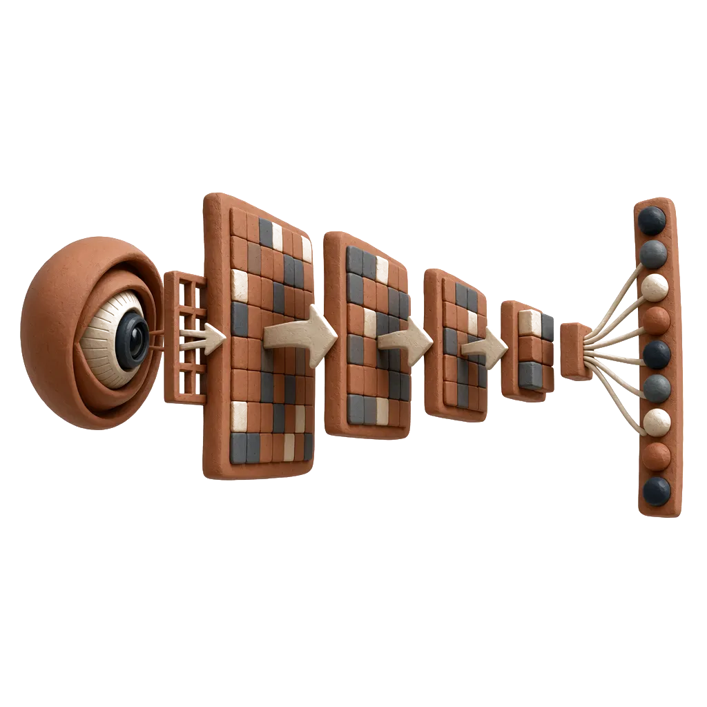
This paper introduces SP&A-Net, a novel neural network architecture combining self-proliferation and attention mechanisms, designed for efficient and accurate semiconductor defect classification suitable for edge devices in IoT-enabled manufacturing.
Contribution
The paper proposes a new neural network architecture that enhances defect classification efficiency and accuracy by integrating self-proliferation and attention mechanisms, optimized for edge deployment.
Findings
Higher accuracy than existing methods
Lower computational cost
Effective in various defect classification tasks
Abstract
Semiconductor manufacturing is on the cusp of a revolution: the Internet of Things (IoT). With IoT we can connect all the equipment and feed information back to the factory so that quality issues can be detected. In this situation, more and more edge devices are used in wafer inspection equipment. This edge device must have the ability to quickly detect defects. Therefore, how to develop a high-efficiency architecture for automatic defect classification to be suitable for edge devices is the primary task. In this paper, we present a novel architecture that can perform defect classification in a more efficient way. The first function is self-proliferation, using a series of linear transformations to generate more feature maps at a cheaper cost. The second function is self-attention, capturing the long-range dependencies of feature map by the channel-wise and spatial-wise attention…
Peer Reviews
No public reviews on file for this paper yet. If you reviewed it on a platform where reviews are public (OpenReview, ICLR, NeurIPS, ICML), you can paste yours below so the community can read it here.
Code & Models
Videos
No videos yet. Explain this paper in a talk, walkthrough, or lecture? Add one.