Probing Image Potential States on Topological Semimetal Antimony Surface
Jian-Feng Ge, Haimei Zhang, Yang He, Zhihuai Zhu, YauChuen Yam,, Pengcheng Chen, and Jennifer E. Hoffman

TL;DR
This study investigates the image potential states on the Sb(111) surface, revealing discrete energy levels and local interactions, which could inform future topological insulator surface manipulations.
Contribution
It provides the first detailed experimental observation of IPS on a topological semimetal surface and explores their spatial variation and interactions.
Findings
Five discrete IPS observed with well-defined energies
Spatial variation indicates resonant interband scattering
Potential for manipulating magnetic charges on TI surfaces
Abstract
A point charge near the surface of a topological insulator (TI) with broken time-reversal symmetry is predicted to generate an image magnetic charge in addition to an image electric charge. We use scanning tunneling spectroscopy to study the image potential states (IPS) of the topological semimetal Sb(111) surface. We observe five IPS with discrete energy levels that are well described by a one-dimensional model. The spatial variation of the IPS energies and lifetimes near surface step edges shows the first local signature of resonant interband scattering between IPS, which suggests that image charges too may interact. Our work motivates the exploration of the TI surface geometry necessary to realize and manipulate a magnetic charge.
Click any figure to enlarge with its caption.
 Figure 1
 Figure 2
 Figure 3
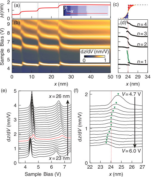 Figure 4
 Figure 5
 Figure 6
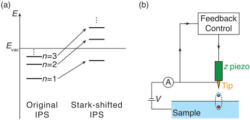 Figure 1
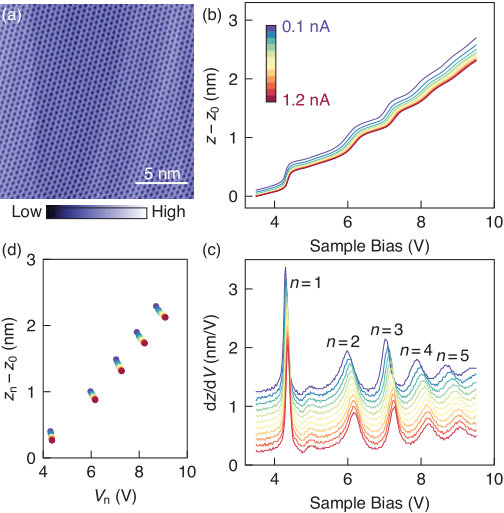 Figure 2
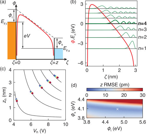 Figure 3
 Figure 4
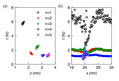 Figure 5
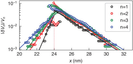 Figure 6
| (nm) | (nm) | |
|---|---|---|
| 0.52 0.05 | 1.84 0.08 | |
| 0.84 0.04 | 1.84 0.05 | |
| 0.89 0.04 | 1.83 0.04 | |
| 1.18 0.04 | 1.91 0.05 |
Peer Reviews
No public reviews on file for this paper yet. If you reviewed it on a platform where reviews are public (OpenReview, ICLR, NeurIPS, ICML), you can paste yours below so the community can read it here.
Videos
No videos yet. Explain this paper in a talk, walkthrough, or lecture? Add one.
Probing Image Potential States on the Topological Semimetal Antimony
Jian-Feng Ge
Department of Physics, Harvard University, Cambridge, MA 02138, USA
Haimei Zhang
School of Engineering and Applied Science, Harvard University, Cambridge, MA, 02138, USA
Department of Physics, Wellesley College, Wellesley, MA 02481, USA
Yang He
Department of Physics, Harvard University, Cambridge, MA 02138, USA
Zhihuai Zhu
Department of Physics, Harvard University, Cambridge, MA 02138, USA
Yau Chuen Yam
Department of Physics, Harvard University, Cambridge, MA 02138, USA
Department of Physics and Astronomy, University of British Columbia, Vancouver, British Columbia V6T 1Z4, Canada
Pengcheng Chen
Department of Physics, Harvard University, Cambridge, MA 02138, USA
Jennifer E. Hoffman
Department of Physics, Harvard University, Cambridge, MA 02138, USA
School of Engineering and Applied Science, Harvard University, Cambridge, MA, 02138, USA
Abstract
A point charge near the surface of a topological insulator (TI) with broken time-reversal symmetry is predicted to generate an image magnetic charge in addition to an image electric charge. We use scanning tunneling spectroscopy to study the image potential states (IPS) of the topological semimetal Sb(111) surface. We observe five IPS with discrete energy levels that are well described by a one-dimensional model. The spatial variation of the IPS energies and lifetimes near surface step edges shows the first local signature of resonant interband scattering between IPS, which suggests that image charges too may interact. Our work motivates the exploration of the TI surface geometry necessary to realize and manipulate a magnetic charge.
1The surface states of topological materials are spin-momentum locked, which reduces the local degrees of freedom and promotes an unusual electromagnetic response. In any material with conducting surface, when an electronic charge is located just outside the material, screening from surface charge will mimic an image electric charge Jackson (1975). In a topological material, as in a normal metal, the attractive potential between the real and image charges can give rise to bound states known as image potential states (IPS) Echenique and Uranga (1991). However, in the topological material, the magnetic and electric degrees of freedom are additionally coupled by the topological magnetoelectric effect Qi et al. (2008). This effect opens a gap in the surface spectrum when time-reversal symmetry is broken, inducing a quantized Hall current and an effective magnetic monopole Qi et al. (2009). Thus the IPS in topological materials with broken time-reversal symmetry exhibit a combined image electric charge and image magnetic charge, which could be controlled by manipulating the real external electric charge near the surface. The manipulation of magnetic monopoles suggests possible applications such as circuitry based on magnetic charges Giblin et al. (2011).
2Understanding the image electrical charge in topological materials is necessary to realize and control the image magnetic charge. The Coulomb potential between the external electric charge and its image results in a Rydberg series of energy levels below the vacuum energy level
[TABLE]
where is a correction factor of the crystal field Echenique et al. (2002). Moreover, a strong electric field can alter due to the Stark effect Crampin (2005). As a result, is no longer a converging series below , but the levels shift to higher energy and spread farther apart, as shown in Fig. 1(a).
3IPS have been well studied by spectroscopic measurements using scanning tunneling microscopy (STM) on metal surfaces Binnig et al. (1985); Wahl et al. (2003); Pivetta et al. (2005); Dougherty et al. (2007), but IPS on topological materials were observed only recently by photoemission Niesner et al. (2012); Sobota et al. (2012, 2013); Niesner et al. (2014a, b); Reimann et al. (2014); Datzer et al. (2017) and force microscopy Yildiz et al. (2019), and have not yet been extensively characterized with local spectroscopy. Here we use spectroscopic STM to investigate IPS on the (111) surface of the topological semimetal Sb. Because of the typical electric field on order 1 V/nm applied between the tip and sample, the IPS are all Stark-shifted. We use spectroscopy to characterize the interaction of the external charge with the topological surface states, by quantifying the change in Stark shift with tip-sample junction setup conditions. Then we show how IPS from distinct terraces evolve across a step edge, and we demonstrate the first localized signature of resonant interband scattering. Our observations suggest a route to engineering interactions between images charges in topological materials.
4Single crystals of Sb were cleaved in cryogenic ultra-high vacuum then loaded directly into our home-built STM. All measurements were carried out at 5 K with mechanically cut PtIr tips cleaned by field emission on Au. The observed (111) plane is atomically flat and free of defects in the 15 nm 15 nm area shown in Fig. 2(a). The experimental setup is illustrated in Fig. 1(b). In spectroscopy, the STM operates in constant-current mode, where the feedback loop controls the tip-sample distance to maintain a constant current . As the bias voltage is increased, the tip is gradually pulled away from the sample. When is tuned in resonance with a Stark-shifted IPS level, there is an instantaneous increase in transmission probability and hence the current. This increase in current leads to an abrupt retraction of the tip, manifested in a spectrum as steps at resonance voltages .
5We searched for IPS in spectroscopic measurements on the Sb(111) surface with a set of tunneling currents ranging from 0.1 nA to 1.2 nA, as shown in Fig. 2(b). As the absolute tip-sample distance is unknown, we define a reference tip-sample distance for the particular setup condition of 3.5 V and 1.2 nA, and we report the measured consistently relative to the same . Each spectrum shows a series of steps at IPS resonance voltages superimposed on a gradually increasing background. We observe two shifts of the spectra as the current increases: the whole spectrum shifts down in the vertical axis; and the steps shift to the right in the horizontal axis. The shift in can be understood as the tip being pushed towards the sample to achieve a higher current set point at the same bias voltage. The shift in is the consequence of the Stark effect: with an increasing current (and thus decreasing ), the electric field increases and shifts the IPS to higher energies and farther apart.
6In order to visualize IPS energy shifts more clearly, we numerically differentiate the spectra and plot the curves in Fig. 2(c). By counting the number of peaks, we observe five IPS up to 9.5 V. We fit each peak in Fig. 2(c) with a Lorentzian function and obtain from the centers of the Lorentzian peaks. Comparing Figs. 2(b) and (c), we extract relative to at each peak voltage and plot the values in Fig. 2(d). Fig. 2(d) shows that the Stark shift increases nonlinearly with increasing current and differs for each level index . We also note that the peak width generally increases at higher . The broadening of IPS peaks can be understood by elastic scattering of IPS electrons into the bulk continuum Pascual et al. (2007).
7To quantitatively understand the data in Fig. 2(d), we use a one-dimensional (1D) model to describe the electrical potential in the vacuum space between tip and sample, assuming that the radius of the tip is much larger than the absolute tip-sample distance Wahl et al. (2003). The 1D potential , as plotted in Fig. 3(a), is the sum of the linear electrostatic potential from the bias of the STM tunnel junction, the image potential of the tip, and the image potential of the sample Pitarke et al. (1990)
[TABLE]
In Eq. 2, the variable is the 1D spatial coordinate, which has an origin at the surface of the tip (), is expressed relative to Fermi level of the tip , is a factor that accounts for all image charges Simmons (1964), and is the vacuum permittivity. The parameter is the bias voltage applied to the sample with respect to tip. There are three unknown parameters: is the absolute tip-sample distance, and are work functions of the tip and the sample, respectively.
We use the potential to solve the 1D Schrödinger equation numerically with the Numerov method Numerov (1927) and find the resonance condition where coincides with the Fermi level of the tip , i.e. . Figure 3(b) shows an example of seven derived eigenenergies and eigenwavefunctions with parameters 8.2 V, 3.0 nm. A resonance at the IPS () indicates 8.2 V, 3.0 nm, which can be compared to our data points in Fig. 2(d) with an adjustable parameter . We fit the data in Fig. 2(d) using the method of least squares for each pair of and in the grid shown in Fig. 3(d), to minimize the root-mean-square error (RMSE) in between all experimental data in Fig. 2(d) and the model result. The best fit with minimal RMSE shown in Fig. 3(c) gives fit parameters 4.79 eV, 4.08 eV, and the offset 1.26 nm. Our and show reasonable agreement with the work functions of Au 5.1 eV (which likely coats the tip after field emission) and Sb 4.55-4.7 eV Michaelson (1977), respectively.
8We next investigate the influence of surface defects on the IPS. Figure 4 shows laterally resolved IPS along a line across three surface steps.
We observe bi-atomic-layer steps of height 4 Å, as shown in Fig. 4(a), consistent with previous reports Gomes et al. (2009); Seo et al. (2010); Yam et al. (2018). We acquire spectra at each point on a line [inset of Fig. 4(a)], and plot the map in Fig. 4(b). The energies of all the IPS peaks are constant far from the step edges but bend to higher (lower) energy near a step edge on the higher (lower) terrace. Despite the different terrace widths, the bipolar bending appears identical near all three step edges in map. Similar bipolar bending has been observed in nanostructures such as NaCl/Ag(100) Ploigt et al. (2007), Co/Au(111) Schouteden and Van Haesendonck (2009), Li/Cu(100) Stepanow et al. (2011), and defects on InAs(111) Martínez-Blanco et al. (2015), and is attributed to the change of surface potential between different materials Ploigt et al. (2007); Schouteden and Van Haesendonck (2009); Zeljkovic et al. (2013). The fact that we see the bipolar bending of IPS on the elementary material Sb indicates a local variation of chemical potential near a step edge. This variation can be understood by the Smoluchowski effect Smoluchowski (1941) as illustrated in Fig. 4(c), where positive and negative charge builds up on the upper and lower edges of a step, respectively. The charge redistribution gives rise to a local dipole moment, which effectively acts as a lateral perturbation to the model potential in Eq. 2 Clinton et al. (1985).
9We extract the IPS peak voltages in the same way as in Fig. 2, and plot these as a function of distance in the -direction in Fig. 4(d). The bipolar bending follows approximately an exponential decay in , with a decay length on the order of 1 nm [see Fig. 6 in Appendix]. We also notice near the step edge each IPS peak splits into two, as exemplified in Fig. 4(e). Although the bipolar bending of IPS has been observed, this splitting of IPS near a step edge has not been clearly characterized before. We speculate that this splitting may stem from the Stark effect caused by the additional local dipole moment or spilling of IPS electrons from one side of the step to the other Schouteden and Van Haesendonck (2009).
10More interestingly, we observed an extra peak that departs from the state on the lower terrace towards the state on the higher terrace. This transition peak is most obvious for in Fig. 4(b), and it is localized within 2 nm across the step as shown by green markers in Fig. 4(d) and Fig. 4(f). For higher , due to the increased width of the IPS peaks, it is difficult to distinguish between the transition peaks and the bending IPS. This transition peak from to , which appears only in the upstairs direction, is a clear signature of resonant interband scattering Fauster et al. (2007). The directional preference in resonant interband scattering was previously noted in photoemission experiments on the stepped Cu(119) surface Roth et al. (2002). This cross-step scattering between distinct IPS states may provide a means to control the interaction between the expected induced magnetic charges when a magnetic layer is deposited on the stepped surface of a topological material Qi et al. (2009).
11We now discuss the spatial evolution of the decay rate of the image charges. The lifetime of IPS can be estimated by , where is the full width at half maximum of the IPS peak Echenique et al. (2004). From the data in Fig. 2(c) and Fig. 3(c) acquired far from a step edge, we plot as a function of tip-sample distance in Fig. 5(a). The IPS electrons live longer than those with higher , as the peak broadening due to inelastic decay increases dramatically for energies above Crampin (2006). We note that with increasing tip-sample distance, IPS lifetime increases for and , but decreases for . Compared to IPS lifetime of fs on topological insulator SnSb2Te4 Niesner et al. (2014a), and 10-15 fs on Bi2Te3 Yildiz et al. (2019), the short IPS lifetime 6 fs on Sb(111) can be attributed to the vanishing negative band gap in semimetal Sb and high availability of bulk states for IPS to scatter elastically into Niesner et al. (2014b). We also extract from Fig. 4 the lateral dependence of IPS lifetime across a step edge in Fig. 5(b). For IPS electrons, the lifetime drops near the step edge by 15% on the lower terrace but by as much as 50% on the upper terrace. The sizable asymmetry of our observed IPS lifetime is reminiscent of the finding on conventional Cu(119) that electrons running upstairs live longer than electrons running downstairs; the similarity can be taken as another piece of evidence for step-induced resonant interband scattering Roth et al. (2002).
12In summary, we observed the first five IPS up to 9.5 V on the topological semimetal Sb(111) surface. The Stark-shifted IPS levels show good quantitative agreement with a simple 1D model that has been used to describe IPS on conventional metals. Additionally, laterally resolved IPS across surface steps show bipolar bending of the IPS levels and the first local signature of resonant interband scattering between IPS. Our study of IPS enriches the understanding of interacting image electrical charges on surfaces of topological materials, and paves the way towards the study of the associated magnetic charges and their interactions.
Acknowledgements.
Experiments were supported by National Science Foundation DMR-1410480, and data analysis was supported by the Science and Technology Center for Integrated Quantum Materials under NSF DMR-1231319. We thank D. R. Gardner and Y. S. Lee for providing Sb single crystals, and we thank D. Yildiz for helpful conversations.
Appendix A Appendix: Details of spatial dependence of IPS near a step edge
Here we extract the spatial dependence of energy bending , where we take average values of for to nm as . We demonstrate in Fig. 6 the exponential decay of the relative energy bending as a function of near the step edge at 24 nm. Note is negative on the left side of the step edge and its absolute value is displayed. We fit separately the data points on left and right sides with an exponential function , where is the decay length on the downstairs (left) or upstairs (right) side of the step edge. The fitted decay lengths for different are summarized in Tab. 1. The decay length is also asymmetric with respect to the step. On the downstairs side of the step edge the the energy bending decays faster than that on the upstairs side by a factor of 2 to 3. This asymmetry may arise from the potential distribution across the step edge.
The reference list from the paper itself. Each links out to its DOI / PubMed record.
- 1Jackson (1975) J.D. Jackson, Classical electrodynamics (Wiley, 1975).
- 2Echenique and Uranga (1991) P.M. Echenique and M.E. Uranga, “Image potential states at surfaces,” Surface Science 247 , 125 – 132 (1991) . · doi ↗
- 3Qi et al. (2008) Xiao-Liang Qi, Taylor L. Hughes, and Shou-Cheng Zhang, “Topological field theory of time-reversal invariant insulators,” Physical Review B 78 , 195424 (2008) . · doi ↗
- 4Qi et al. (2009) Xiao-Liang Qi, Rundong Li, Jiadong Zang, and Shou-Cheng Zhang, “Inducing a magnetic monopole with topological surface states,” Science 323 , 1184–1187 (2009) . · doi ↗
- 5Giblin et al. (2011) SR Giblin, ST Bramwell, PCW Holdsworth, D Prabhakaran, and I Terry, “Creation and measurement of long-lived magnetic monopole currents in spin ice,” Nature Physics 7 , 252 (2011) . · doi ↗
- 6Echenique et al. (2002) P.M. Echenique, J.M. Pitarke, E.V. Chulkov, and V.M. Silkin, “Image-potential-induced states at metal surfaces,” Journal of Electron Spectroscopy and Related Phenomena 126 , 163 – 175 (2002) . · doi ↗
- 7Crampin (2005) S. Crampin, “Lifetimes of Stark-shifted image states,” Physical Review Letters 95 , 046801 (2005) . · doi ↗
- 8Binnig et al. (1985) G Binnig, K H Frank, H Fuchs, N Garcia, B Reihl, H Rohrer, F Salvan, and A R Williams, “Tunneling spectroscopy and inverse photoemission: image and field states,” Physical Review Letters 55 , 991–994 (1985) . · doi ↗