Rigid band shifts in two-dimensional semiconductors through environmental screening
Lutz Waldecker, Archana Raja, Malte R\"osner, Christina Steinke, Aaron, Bostwick, Roland J. Koch, Chris Jozwiak, Takashi Taniguchi, Kenji Watanabe,, Eli Rotenberg, Tim O. Wehling, Tony F. Heinz

TL;DR
This study demonstrates that environmental dielectric screening causes primarily rigid band gap reductions in 2D WS$_2$, with minimal impact on electronic dispersion, highlighting dielectric engineering as a tool for tuning 2D semiconductor properties.
Contribution
It provides experimental and theoretical evidence that dielectric environment induces mainly rigid band shifts in 2D semiconductors, informing future material engineering strategies.
Findings
Band gap reduction due to increased dielectric screening
Minimal change in electronic dispersion
Guidance for dielectric engineering in 2D materials
Abstract
We investigate the effects of environmental dielectric screening on the electronic dispersion and the band gap in the atomically-thin, quasi two-dimensional (2D) semiconductor WS using correlative angle-resolved photoemission and optical spectroscopies, along with first-principles calculations. We find the main effect of increased environmental screening to be a reduction of the band gap, with little change to the electronic dispersion of the band structure. These essentially rigid shifts of the bands results from the special spatial structure of the changes in the Coulomb potential induced by the dielectric environment in the 2D limit. Our results suggest dielectric engineering as a non-invasive method of tailoring the band structure of 2D semiconductors and provide guidance for understanding the electronic properties of 2D materials embedded in multilayer heterostructures.
Click any figure to enlarge with its caption.
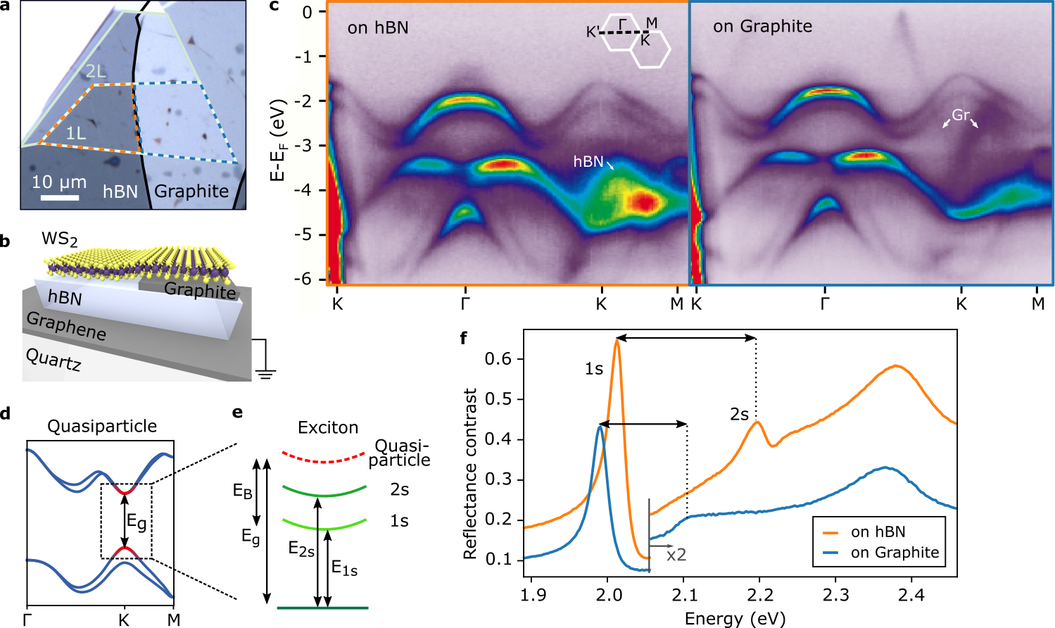 Figure 1
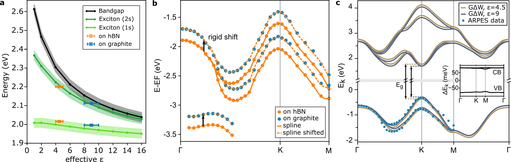 Figure 2
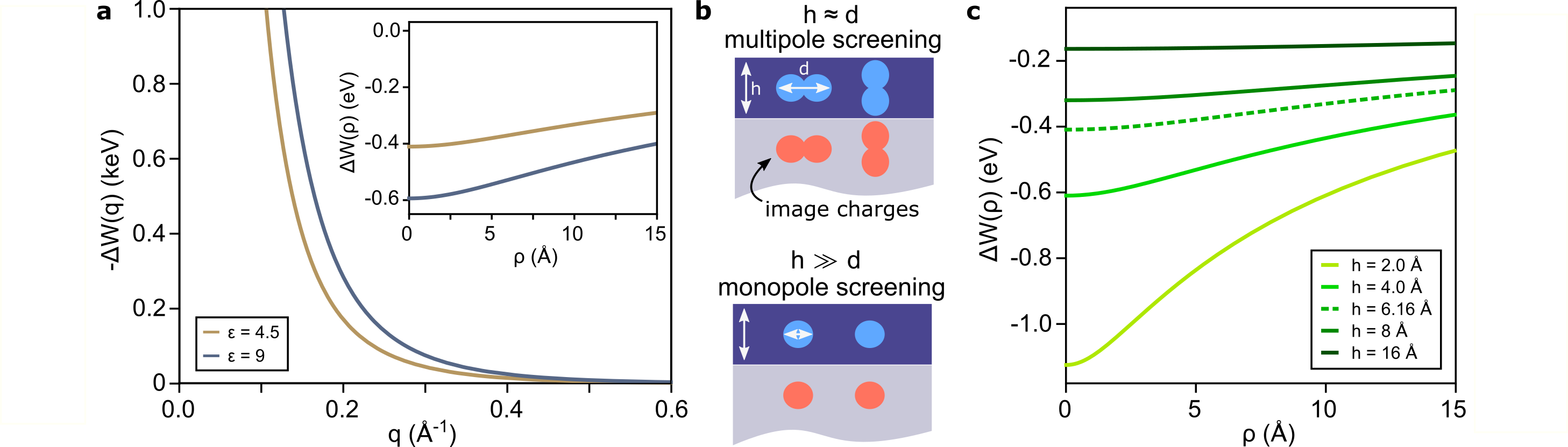 Figure 3
Peer Reviews
No public reviews on file for this paper yet. If you reviewed it on a platform where reviews are public (OpenReview, ICLR, NeurIPS, ICML), you can paste yours below so the community can read it here.
Videos
No videos yet. Explain this paper in a talk, walkthrough, or lecture? Add one.
\DefineFNsymbolsTM
otherfnsymbols††‡‡§§
Rigid band shifts in two-dimensional semiconductors through environmental screening
Lutz Waldecker∗
Dept. of Applied Physics, Stanford University, 348 Via Pueblo Mall, Stanford, California 94305, USA
SLAC National Accelerator Laboratory, Menlo Park, California 94025, USA
Archana Raja∗
Dept. of Applied Physics, Stanford University, 348 Via Pueblo Mall, Stanford, California 94305, USA
SLAC National Accelerator Laboratory, Menlo Park, California 94025, USA
Kavli Energy NanoScience Institute, University of California Berkeley, Berkeley, California 94720, USA
Malte Rösner∗
Institute for Molecules and Materials, Radboud University, 6525 AJ Nijmengen, The Netherlands
Christina Steinke
Institute for Theoretical Physics, University of Bremen, Otto-Hahn-Allee 1, 28359 Bremen, Germany
Bremen Center for Computational Material Sciences, University of Bremen, Am Fallturm 1a, 28359 Bremen, Germany
Aaron Bostwick
Roland J. Koch
Chris Jozwiak
Advanced Light Source, E. O. Lawrence Berkeley National Laboratory, Berkeley, California 94720, USA
Takashi Taniguchi
Kenji Watanabe
National Institute for Materials Science, Tsukuba, Ibaraki 305-004, Japan
Eli Rotenberg
Advanced Light Source, E. O. Lawrence Berkeley National Laboratory, Berkeley, California 94720, USA
Tim O. Wehling
Institute for Theoretical Physics, University of Bremen, Otto-Hahn-Allee 1, 28359 Bremen, Germany
Bremen Center for Computational Material Sciences, University of Bremen, Am Fallturm 1a, 28359 Bremen, Germany
Tony F. Heinz
Dept. of Applied Physics, Stanford University, 348 Via Pueblo Mall, Stanford, California 94305, USA
SLAC National Accelerator Laboratory, Menlo Park, California 94025, USA
Abstract
We investigate the effects of environmental dielectric screening on the electronic dispersion and the band gap in the atomically-thin, quasi two-dimensional (2D) semiconductor WS2 using correlative angle-resolved photoemission and optical spectroscopies, along with first-principles calculations. We find the main effect of increased environmental screening to be a reduction of the band gap, with little change to the electronic dispersion of the band structure. These essentially rigid shifts of the bands results from the special spatial structure of the changes in the Coulomb potential induced by the dielectric environment in the 2D limit. Our results suggest dielectric engineering as a non-invasive method of tailoring the band structure of 2D semiconductors and provide guidance for understanding the electronic properties of 2D materials embedded in multilayer heterostructures.
In monolayers of atomically-thin, quasi two-dimensional (2D) semiconductors, the intrinsic screening of Coulomb interactions is reduced compared to their bulk crystals, since electric field lines between charges extend significantly outside the material. As a result, exciton binding energies are enhanced, reaching values of several hundreds of meV in the transition metal dichalcogenides (TMDCs) Ramasubramaniam (2012); Berkelbach et al. (2013); Qiu et al. (2013); He et al. (2014); Chernikov et al. (2014); Ye et al. (2014); Wang et al. (2018). For the same reason, materials in close proximity to the monolayers enhance the effective screening of charge carrier interactions. By embedding atomically-thin materials in different dielectric environments, their band gaps, as well as exciton binding energies, can therefore be modified on an energy scale of the exciton binding energies themselves Rösner et al. (2016); Stier et al. (2016); Raja et al. (2017). This sensitivity becomes particularly important in vertical heterostructures of 2D materials and enables a non-invasive way of designing nanoscale functionality, such as lateral heterojunctions, through the spatial control of substrate dielectrics Rösner et al. (2016); Raja et al. (2017); Utama et al. (2019).
To exploit the full potential of tailoring Coulomb interactions through control of the dielectric environment, it is critical to understand its impact not only on the band gap but also on the valence and conduction band dispersions. The dispersion determines such basic properties as the effective masses of the carriers and the energy differences between different valleys within the Brillouin zone, and also affects the relative alignment between the valence and conduction bands of a homogeneous monolayer with spatially varying external dielectric screening. To date, experimental studies of dielectric engineering have mainly focused on optical spectroscopy or electronic transport measurements of TMDC monolayers, which only probe a small fraction of the full Brillouin zone. In general, however, perturbations to a material do not have the same effect on electronic states of different orbital character and can be expected to modify the band structure in different parts of the Brillouin zone differently.
Here, through a combination of experiment and theory, we provide a generalized picture of the consequences of dielectric screening for the band structure of 2D semiconductors. By combining angle-resolved photoemission spectroscopy with micrometer spatial resolution (µ-ARPES) and optical spectroscopy of the exciton states of monolayer WS2 on different substrates, we find that the predominant effect of external screening is a band gap renormalization through a rigid shift of the occupied and unoccupied bands relative to each other. These rigid shifts are a result of the spatial structure of the changes in the Coulomb potential induced by the dielectric environment, which we elucidate with the aid of ab initio GW calculations. Our results illustrate how non-local screening in 2D materials can yield a solid state analogue of molecular level renormalization in different solvent environments or on surfaces Neaton et al. (2006); Thygesen and Rubio (2009).
Monolayers of the semiconducting TMDC WS2 were exfoliated from bulk crystals and transferred such that they partially cover two different substrates, hexagonal Boron Nitride (hBN) and graphite (for experimental and sample fabrication details, see Supplementarty Information). An optical micrograph of a typical sample and a schematic of the sample geometry used in the experiments are shown in Figs. 1 a and b.
Using µ-ARPES, we measure the valence band dispersion and the separation to shallow core levels, including W4f. Two examples of room temperature photoemission intensity maps of the valence bands of WS2 in the K’--K-M direction of WS2 are shown in Fig. 1 c. Signatures of the respective substrates appear in both spectra, such as the -band of hBN and replicas of graphite bands extending to the Fermi energy EF. However, no signs of hybridization between WS2 and the respective substrate bands are observed.
By measuring the exciton states on the same samples, we obtain information on quasiparticle band gaps at the K points (Fig. 1 d). Typical reflectance contrast spectra, approximately proportional to the monolayer absorption, are shown in Fig. 1 f. As the oscillator strength in 2D semiconductors mainly resides in their excitonic absorption features, a series of prominent peaks is seen in the spectra. We identify the two lowest lying features as the 1s and 2s exciton states of the A exciton transition Chernikov et al. (2014). While the quasiparticle band gap is not directly accessible, it is proportional to the 1s-2s separation (Fig. 1 e) Chernikov et al. (2014); Raja et al. (2017); Cho and Berkelbach (2018). The exciton binding energy and the quasiparticle band gap are sensitive to dielectric screening from the immediate environment of hBN and graphite, which is reflected in both the shifting of the exciton peaks and, more importantly, the reduction of the 1s-2s separation Raja et al. (2017). This is also evidence of close contact between WS2 and the hBN/graphite substrates. The lack of charged exciton signatures and narrow linewidths in the optical spectra indicate low doping levels Mak et al. (2013), consistent with the ARPES data in which the Fermi level is observed within the band gap.
We now analyze the experimentally measured dispersion and the band gap renormalization in conjunction with first-principles calculations. We calculate the band structure of a freestanding WS2 monolayer in the GW approximation, from which the band gap in vacuum () is obtained (see SI for details) in good agreement with Ref. Haastrup et al. (2018). The change in the band gap is then calculated using a combination of the Wannier function continuum electrostatics (WFCE) Rösner et al. (2015) and GW approaches Rohlfing (2010); Winther and Thygesen (2017), where W is the environmentally-induced change to the Coulomb potential resulting from a dielectric substrate described by an effective dielectric constant . in this way, we reduce the complex dielectric function of the substrates to an effective screening constant , independent of momentum and frequency.
The calculated change of the quasiparticle band gap, i.e. the difference between the valence band maximum and the conduction-band minimum at the K-points, is shown in Fig. 2 a. To compare this result to the measured exciton positions, we additionally solve the Wannier equation for the screened potentials and obtain the binding energies of 1s and 2s exciton states (see SI). We find good agreement between experimental and calculated exciton positions for and for hBN and graphite respectively (see Fig. 2 c). These values are in reasonable agreement with previously reported values Andersen et al. (2015). We note that of the same substrate can be different for other 2D semiconductors. The calculated band gap renormalization upon changing the dielectric substrate from to is found to be 140 meV. We conclude that the band gap of monolayer WS2 on hBN compared to graphite is approximately 140 meV larger.
To elucidate how the environmental screening affects the electronic dispersion, we determine the band positions from the ARPES data in Fig. 1 c by fitting energy distribution curves (EDCs) of the valence bands at each recorded parallel momentum and accounting for detector distortions (see SI). Intriguingly, a spline through the data points on hBN can be rigidly shifted to overlay the data points on graphite within the experimental error of approximately 25 meV. In particular, the relative alignment of the K-points with respect to is determined as 280(280) meV on hBN (graphite) and the spin-orbit splitting at the K-points Zhu et al. (2011) is 440(430) meV. The effective masses in the valence bands are determined from quadratic fits as 2.45(2.55) at , 0.48(0.48) in the upper and 0.64(0.78) in the lower valence band at the K points on hBN (graphite).
The calculated valence- and conduction-band dispersions for the two values of are shown in Fig. 2 c together with the the experimental data points on graphite for comparison. Since the absolute band energies in photoemission can be influenced by external fields, we align the experimental bands to the GW calculations at their -point energies. The calculated curves closely follow the measured dispersion, with small deviations roughly halfway between and K as well as close to M. These discrepancies may arise from the difficulty of fitting two bands where their separation is small, along with approximations used in the calculations. Since deviations occur in a region of strong orbital hybridization, we expect it to be particularly sensitive to small errors in lattice relaxation.
From our calculations of the dispersion, it is clear that the main effect of the environmental screening is a rigid shift of occupied and unoccupied bands, as also observed in Ref. Winther and Thygesen (2017). The shift is symmetric in the valence and conduction bands, which is to first order intrinsic to the 2D slab geometry as discussed in detail later. The change in dispersion is visualized in the inset of Fig. 2 c, where the difference between the band energies is plotted. In the calculations, the deviations from a rigid shift are smaller than 5 meV across the Brillouin zone, which is less than 5% of the band gap renormalization and is consistent with our experimental observations.
These essentially rigid shifts can be understood from the change of the Coulomb interaction profile as resulting from the screening environment with dielectric constant with respect to the interaction of the freestanding layer in vacuum (V) and its effects to the GW band structure (see SI). In Fig. 3 a we show examples for and as functions of the real-space coordinate (inset) and the momentum-transfer . Since is always larger than , is by definition negative. In real space we find nearly constant potential profiles for Å which approaches zero for larger . This behavior of results from the non-local screening properties of the 2D slab with finite height . In the case of purely local screening we expect to diverge for small . Here, however, the two dielectric interfaces (top and bottom side of the WS2 layer) are separated by from the center of the slab and create an alternating infinite series of image charges localized at distances Å. The corresponding contributions to are of the form Cho and Berkelbach (2018) and thus flat at small . Therefore, it is necessary to fully take the effective height into account. The well-known approximation of the Keldysh potential Cudazzo et al. (2011), which is only valid for , is therefore not capable of describing this particular change in interaction profile.
The flat interaction profile in real space translates to a strongly peaked profile in momentum space being zero for . For the following analysis we can thus approximate and . Importantly, this type of interaction does not distinguish between different orbital characters and cannot cause any inter-band scattering.
In this case, the electronic self-energy , which describes the changes in the electronic quasiparticle dispersions in the WS2 layer due to changes in the environmental screening, greatly simplifies in the GW approximation. For electrons in band with momentum it reads
[TABLE]
In the static Coulomb-hole plus screened-exchange (COHSEX) approximation, this self-energy can be split into two terms resulting from poles in and in yielding and , respectively, where is the Fermi function. The SEX part shifts only occupied states up in energy and the COH terms shifts all bands down by . Importantly, these self-energies are independent of for completely filled (empty) valence (conduction) bands, since the Fermi functions depend only on band index but not on here. The quasiparticle dispersions under the influence of environmental screening then read
[TABLE]
The bands shift as a whole with no changes to the dispersion and the band gap is symmetrically reduced by equally for all momenta . Experimentally, we observe these rigid shifts down to the core-levels W4f (see SI) and also find them in our full COHSEX calculations [using the full orbital-dependent ] presented in Fig. 2.
In order to change the band shapes or to induce asymmetric band shifts, significant deviations from the approximation are needed. Thus, either must become orbital-dependent, or must break down. This is controlled by the ratio between the effective WS2 height and the orbital extension . For small , for example, the multipole-pole screening by the image charges differentiates between different orbital characters (see Fig. 3 b), and becomes orbital-dependent. Also, for small the change to the Coulomb potential starts to show a spatial structure (see Fig. 3 c), and becomes inaccurate. Thus, by reducing the effective height or increasing the orbital extension, non-rigid-shift modifications may occur. In the case of the TMDCs, the transition metal d orbitals are “shielded” by the surrounding chalcogen atoms which increases the effective height and reduces non-rigid-shift effects. In effectively thinner materials with multi-orbital band-edge characters these effects could, however, be stronger.
Thus the validity of the approximation is an intrinsic property of the monolayer and certainly holds for WS2. We therefore do not expect any deviations from the rigid-shift-like changes to the band structure, even if the environmental screening shows a significant frequency dependence like in the case of graphite Lin et al. (1997). As shown above, there are indeed no additional changes to the valence bands for graphite (Fig.2 b) so that our static theory adequately interpolates the experimental dispersion (Fig.2 c).
In conclusion, we have built a lateral heterojunction by exposing a homogeneous WS2 monolayer to spatially-separated dielectric environments. With the help of our combined experimental-theoretical studies we are able to show that the main change of the electronic properties of WS2 between both environments is a band gap opening and a rigid shift of its valence and conduction bands. The non-local nature of the screening leads to almost constant changes of the Coulomb potential in WS2, which translate to a symmetric opening and closing of the band gap. This mechanism is consistent with recently reported data from transport measurements across a similar dielectrically-engineered lateral heterojunction Utama et al. (2019). The observed rigid shifts are in stark contrast to other methods of band gap engineering, such as ion-doping, in which the upper valence band at K is modified and the spin-splitting of the bands increases Katoch et al. (2017) or the application of strain, which results in a change of the energetic alignment of different valleys Yun et al. (2012); Conley et al. (2013). Our results establish dielectric engineering as a non-invasive way of modifying the quasiparticle band gap of 2D semiconductors and will help understand phenomena on the interfaces between 2D semiconductors and other materials.
I Acknowledgements
We would like to thank Simone Latini for helpful hints for solving the 2D Schrödinger equation. The spectroscopic studies were supported by the US Department of Energy, Office of Science, Basic Sciences, Materials Sciences and Engineering Division, under Contract DE-AC02-76SF00515 for analysis and by the Gordon and Betty Moore Foundation’s EPiQS Initiative through Grant No. GBMF4545. L.W. and M.R. acknowledge support by the Alexander von Humboldt Foundation. A.R. gratefully acknowledges funding through the Heising-Simons Junior Fellowship within the Kavli Energy NanoScience Institute at the University of California, Berkeley. T.W. and C.S. acknowledge support by the European Graphene Flagship and DFG via GRK 2247. K.W. and T.T. acknowledge support from the Elemental Strategy Initiative conducted by the MEXT, Japan, A3 Foresight by JSPS and the CREST (JPMJCR15F3), JST. This research used resources of the Advanced Light Source, which is a DOE Office of Science User Facility under contract no. DE-AC02-05CH11231.
The reference list from the paper itself. Each links out to its DOI / PubMed record.
- 1Ramasubramaniam (2012) A. Ramasubramaniam, Physical Review B 86 , 115409 (2012) . · doi ↗
- 2Berkelbach et al. (2013) T. C. Berkelbach, M. S. Hybertsen, and D. R. Reichman, Physical Review B 88 , 045318 (2013) . · doi ↗
- 3Qiu et al. (2013) D. Y. Qiu, F. H. Da Jornada, and S. G. Louie, Physical Review Letters 111 , 216805 (2013) . · doi ↗
- 4He et al. (2014) K. He, N. Kumar, L. Zhao, Z. Wang, K. F. Mak, H. Zhao, and J. Shan, Physical Review Letters 113 , 026803 (2014) . · doi ↗
- 5Chernikov et al. (2014) A. Chernikov, T. C. Berkelbach, H. M. Hill, A. Rigosi, Y. Li, O. B. Aslan, D. R. Reichman, M. S. Hybertsen, and T. F. Heinz, Physical Review Letters 113 , 076802 (2014) . · doi ↗
- 6Ye et al. (2014) Z. Ye, T. Cao, K. O’Brien, H. Zhu, X. Yin, Y. Wang, S. G. Louie, and X. Zhang, Nature 513 , 214 (2014) . · doi ↗
- 7Wang et al. (2018) G. Wang, A. Chernikov, M. M. Glazov, T. F. Heinz, X. Marie, T. Amand, and B. Urbaszek, Reviews of Modern Physics 90 , 21001 (2018) . · doi ↗
- 8Rösner et al. (2016) M. Rösner, C. Steinke, M. Lorke, C. Gies, F. Jahnke, and T. O. Wehling, Nano Letters 16 , 2322 (2016) . · doi ↗