The Electronic Thickness of Graphene
Peter Rickhaus, Ming-Hao Liu, Marcin Kurpas, Annika Kurzmann, and Yongjin Lee, Hiske Overweg, Marius Eich, Riccardo Pisoni and, Takashi Tamaguchi, Kenji Wantanabe, Klaus Richter, Klaus Ensslin and, Thomas Ihn

TL;DR
This study measures the effective electronic thickness of graphene layers by analyzing electrostatic coupling and quantum capacitance, revealing a finite dielectric thickness and decoupled layers with large Fermi wavelengths, supported by experimental and theoretical results.
Contribution
It introduces a method to determine the finite dielectric thickness of graphene layers through electrostatic measurements and confirms the decoupled nature of twisted graphene layers with large Fermi wavelengths.
Findings
Measured dielectric thickness of graphene as 2.6 Å.
Demonstrated decoupling of layers with large Fermi wavelengths.
Reproduced results with tight-binding calculations.
Abstract
The van-der-Waals stacking technique enables the fabrication of heterostructures, where two conducting layers are atomically close. In this case, the finite layer thickness matters for the interlayer electrostatic coupling. Here we investigate the electrostatic coupling of two graphene layers, twisted by 22 degrees such that the layers are decoupled by the huge momentum mismatch between the K and K' points of the two layers. We observe a splitting of the zero-density lines of the two layers with increasing interlayer energy difference. This splitting is given by the ratio of single-layer quantum capacitance over interlayer capacitance C and is therefore suited to extract C. We explain the large observed value of C by considering the finite dielectric thickness d of each graphene layer and determine d=2.6 Angstrom. In a second experiment we map out the entire density range with a…
Click any figure to enlarge with its caption.
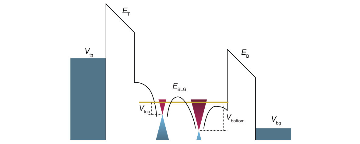 Figure 1
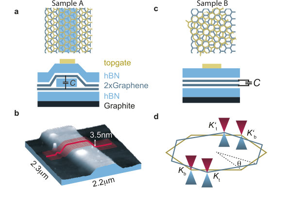 Figure 0
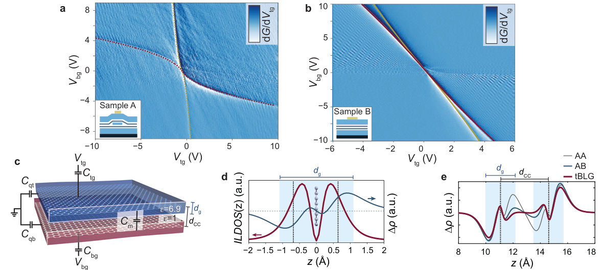 Figure 1
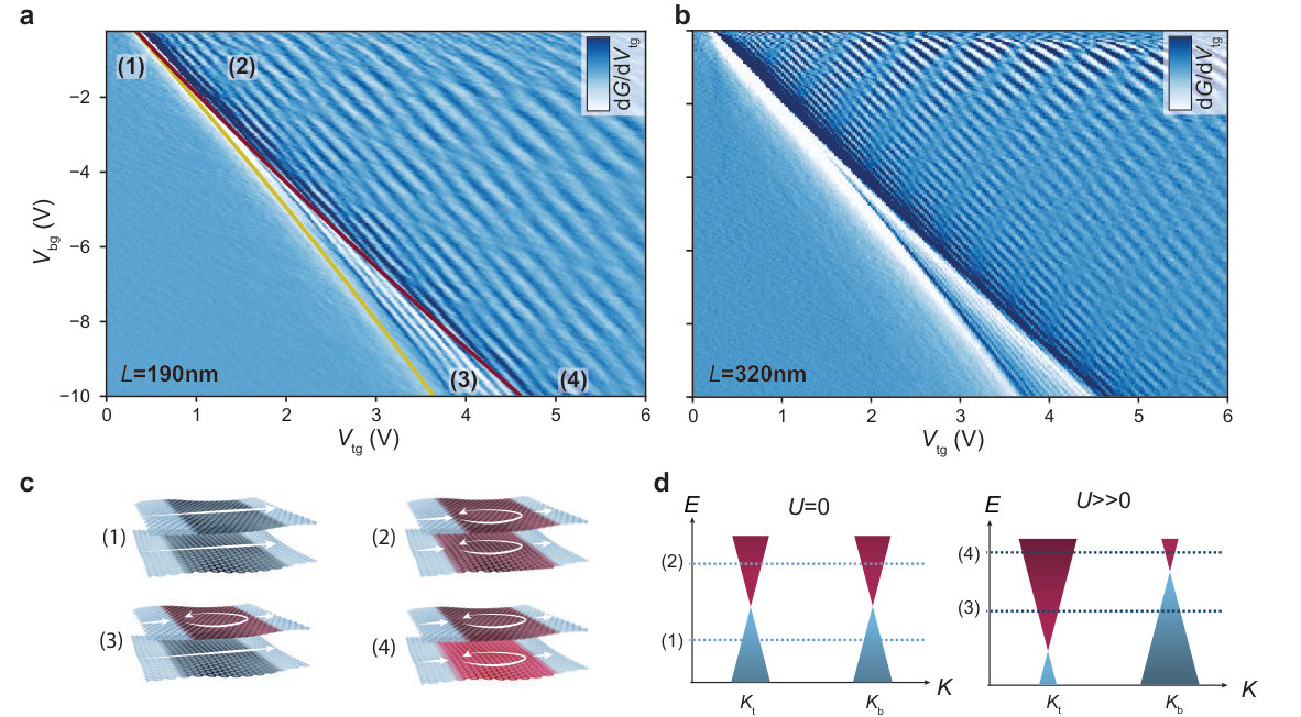 Figure 2
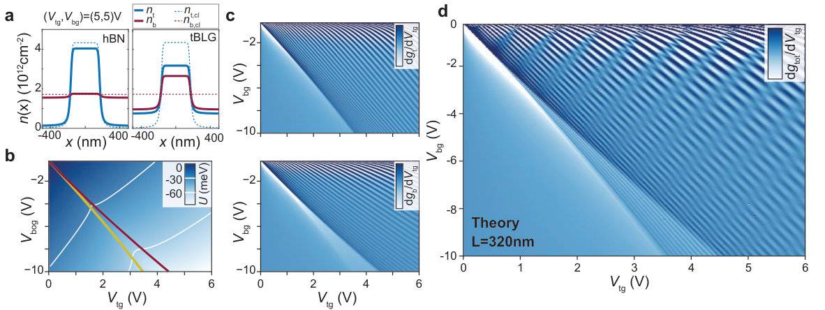 Figure 3
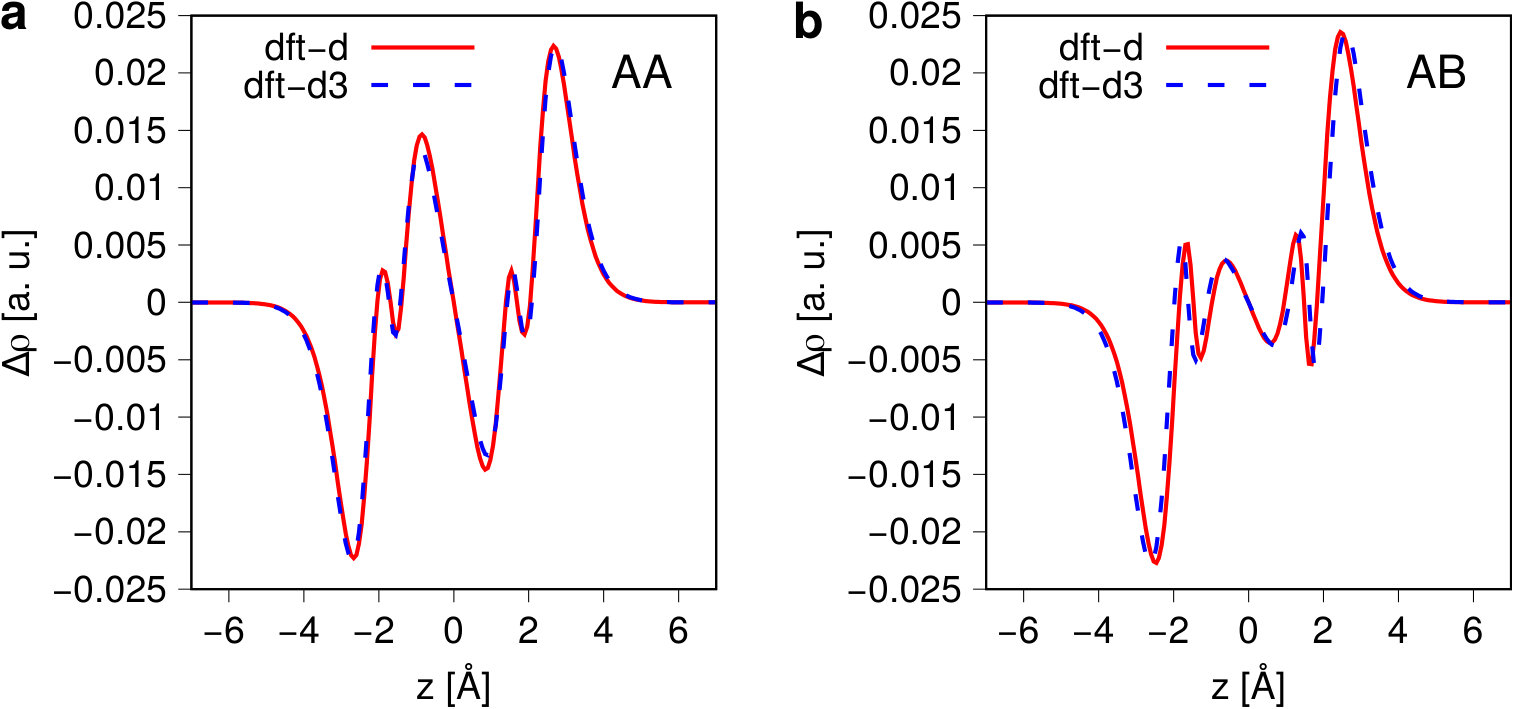 Figure 6
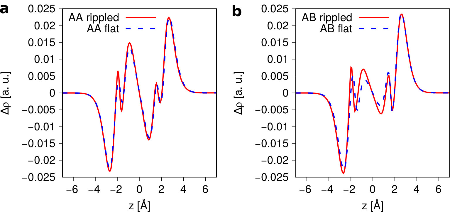 Figure 7
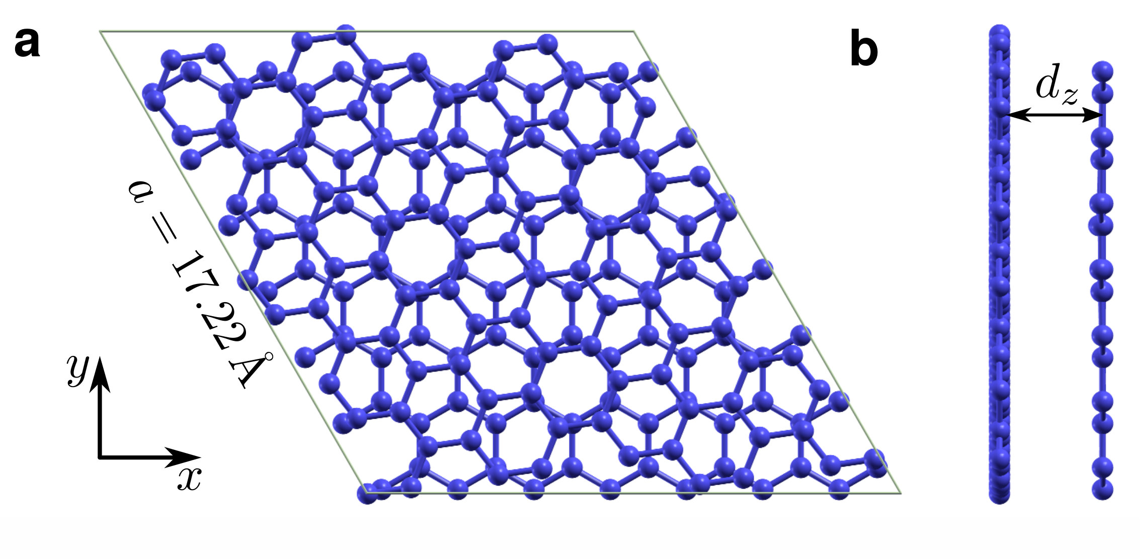 Figure 8
 Figure 1
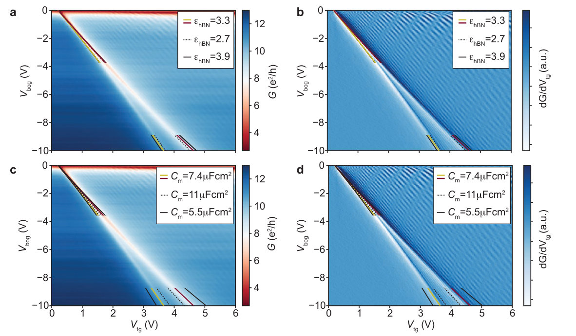 Figure 2
| AA DFT-D | AA DFT-D3 | AB DFT-D | AB DFT-D3 |
| 3.536 Å | 3.64 Å | 3.24 Å | 3.51 Å |
Peer Reviews
No public reviews on file for this paper yet. If you reviewed it on a platform where reviews are public (OpenReview, ICLR, NeurIPS, ICML), you can paste yours below so the community can read it here.
Videos
No videos yet. Explain this paper in a talk, walkthrough, or lecture? Add one.
The Electronic Thickness of Graphene
Peter Rickhaus
Solid State Physics Laboratory, ETH Zürich, CH-8093 Zürich, Switzerland
Ming-Hao Liu
Department of Physics, National Cheng Kung University, Tainan 70101, Taiwan
Marcin Kurpas
Institute of Physics, University of Silesia in Katowice, 41-500 Chorzów, Poland
Annika Kurzmann
Yongjin Lee
Hiske Overweg
Marius Eich
Riccardo Pisoni
Solid State Physics Laboratory, ETH Zürich, CH-8093 Zürich, Switzerland
Takashi Tamaguchi
Kenji Wantanabe
National Institute for Material Science, 1-1 Namiki, Tsukuba 305-0044, Japan
Klaus Richter
Institute for Theoretical Physics, University of Regensburg, D-93040 Regensburg, Germany
Klaus Ensslin
Thomas Ihn
Solid State Physics Laboratory, ETH Zürich, CH-8093 Zürich, Switzerland
Abstract
The van-der-Waals stacking technique enables the fabrication of heterostructures, where two conducting layers are atomically close. In this case, the finite layer thickness matters for the interlayer electrostatic coupling. Here we investigate the electrostatic coupling of two graphene layers, twisted by 22\text{,}\mathrm{\SIUnitSymbolDegree} such that the layers are decoupled by the huge momentum mismatch between the K and K’ points of the two layers. We observe a splitting of the zero-density lines of the two layers with increasing interlayer energy difference. This splitting is given by the ratio of single-layer quantum capacitance over interlayer capacitance $C_{\mathrm{m}}$ and is therefore suited to extract $C_{\mathrm{m}}$. We explain the large observed value of $C_{\mathrm{m}}$ by considering the finite dielectric thickness $d_{\mathrm{g}}$ of each graphene layer and determine $d_{\mathrm{g}}\approx$2.6\text{\,}\mathrm{\SIUnitSymbolAngstrom}. In a second experiment we map out the entire density range with a Fabry-Pérot resonator. We can precisely measure the Fermi-wavelength in each layer, showing that the layers are decoupled. We find that exceeds at the lowest densities and can differ by an order of magnitude between the upper and lower layer. These findings are reproduced using tight-binding calculations.
The van-der-Waals stacking technique allows scientists to bring two conductive crystalline layers into atomically close proximity Novoselov et al. (2016). This has been exploited in a variety of experiments, including the formation of layer polarized, counter-propagating Landau levelsSanchez-Yamagishi et al. (2017) and experiments that build on strong capacitive coupling such as Coulomb-drag measurements Gorbachev et al. (2012) or interlayer exciton condensationLiu et al. (2017, 2018).
There are two main approaches of how to bring two conductive layers in close proximity, while suppressing an overlap of the layer wavefunctions: One approach introduces a thin layer of hexagonal Boron-Nitride (hBN) (see e.g. Gorbachev et al. (2012); Greenaway et al. (2015); Liu et al. (2017)) as depicted in Fig. 1a,b, and the other twists the layers by a large angle () Luican et al. (2011); Rozhkov et al. (2016); Sanchez-Yamagishi et al. (2012, 2017); see Fig. 1c,d. In the former case, decoupling is achieved by spatial separation. In the latter case, the layers are ultimately close, but they remain decoupled due to a large momentum mismatch between the upper and lower layer (Fig. 1d). Experimental signatures of decoupling are an increased interlayer resistanceChari et al. (2016); Ribeiro-Palau et al. (2018) and layer-polarized Landau-levels at large magnetic fields Sanchez-Yamagishi et al. (2012, 2017).
In this work we perform quantum transport experiments to monitor precisely the coupling, coherence and tunability of two graphene layers which are in close proximity to each other. In one device we separate the two layers by a thin layer of hBN with thickness 3.5\text{,}\mathrm{n}\mathrm{m}$$ (sample A) and in the other device we twist the layers by in order to decouple them (sample B).
In the first experiment we observe a splitting of the charge neutrality points of the two layers in the parameter plane of top- and back gate voltage (, ). By analyzing the splitting we extract a geometric capacitance between the graphene layers. For sample A we obtain the expected value given the thickness and dielectric constant of the intermediate hBN layer. However, for sample B, is three times larger than the geometric capacitance between two ideal capacitor plates, separated by the interlayer distance between carbon atoms 3.4\text{,}\mathrm{\SIUnitSymbolAngstrom}$$ assuming vacuum in-between. We argue that, due to the finite electronic thickness of graphene, the plates of the capacitor are effectively closer than leading to the enhanced . We find good agreement with a capacitive model where we take the electronic thickness of graphene into account.
In the second experiment on sample B we use a gate-defined Fabry-Pérot cavity to monitor the layer densities, coherence and interlayer coupling of wavefunctions. The cavities are formed by gate-defined p-n junctions which act as semi-transparent lateral ”mirrors” of the interferometer Liang et al. (2001); Cheianov and Fal’ko (2006); Young and Kim (2009); Rickhaus et al. (2013); Varlet et al. (2014). Either only one or both layers can be tuned to the bipolar p-n-p regime. In both layers we observe the lowest energy Fabry-Pérot mode, corresponding to 600\text{,}\mathrm{n}\mathrm{m}$$, while the wavelength in the other cavity can be shorter by a factor of 10. We model the observed interference pattern using tight-binding calculations assuming completely decoupled layers. This second experiment confirms the assumed electronic decoupling and, for arbitrary gate voltages, the electrostatic model that considers thick graphene.
Methods
In order to achieve ballistic transport, we encapsulateWang et al. (2013) either twisted bilayer graphene (sample B) or graphene-( hBN)-graphene between hBN layers (sample A) and use a graphite bottom gate Zibrov et al. (2017); Overweg et al. (2017). The alignment of the graphene layers is controlled by the method described in Refs. Kim et al. (2016, 2017), and we employed twist angles (between the graphene layers) 0\text{,}\mathrm{\SIUnitSymbolDegree} for sample A and $\theta\approx$22\text{\,}\mathrm{\SIUnitSymbolDegree} for sample B. The thickness of the top, bottom and intermediate hBN layers is determined by atomic force microscopy (AFM). Electrical one-dimensional contacts are achieved by reactive ion etching and evaporation of Cr/Au. Top gates of size and are defined by electron beam lithography. By adjusting the top gate and back gate voltage , a Fabry-Pérot cavitiy can be formed below the top gate. Two-terminal linear conductance measurements are performed using a low-frequency lock-in technique () at the temperature 1.5\text{,}\mathrm{K}$$.
Results
The numerical conductance as a function of and is shown in Fig. 2a for sample A and Fig. 2b for sample B. In both cases two pronounced curved lines are observed, corresponding to a dip in the conductance . The lines cross at zero gate voltages and the splitting between these lines increases with increasing difference in and . One line (following the yellow dashed line) is affected more strongly by the top gate voltage and therefore corresponds to the condition for charge neutrality in the upper graphene layer, whereas the other line (red dashed) indicates charge neutrality in the lower layer.
From electrostatic considerations we find that the zero-density condition can be expressed as (details are given in the Supplemental Material)
[TABLE]
where () is the geometric capacitance of the bottom (top) graphene to the bottom- (top-) gate (see Fig. 2c) and the density in the bottom (top) graphene layer is (). The capacitance measured between the two graphene plates is . The quantum capacitance of the top layer is proportional to the density of states at the Fermi energy in the top layer (the analogue relation holds for the bottom layer). For a single-sheet of graphene, the slope of the zero-density line in a ()-map is given by the ratio (prefactor in the above equations). For the two-layer system, the deviations from linearity of the constant density line are governed by the ratio between quantum capacitance and , respectively. Therefore the splitting is smaller in sample B where is large as compared to sample A, where is smaller.
Analytical formulas for the zero density lines (i.e. and ) can be calculated using the ideal density of states of defect-free graphene and are depicted in Fig. 2a and b for the different electrostatic configuration (i.e. with or without hBN between the graphene sheets). The formulas and details of the calculation are given in the Supplemental Information. Fitting these curves to the data allows us to extract which is the only free fitting parameter. The other capacitances in the problem are given by the thickness of the top/bottom hBN, i.e. with . A discussion for the precision of this method is given in the Supplemental Material. A
For sample A we obtain an interlayer capacitance of 0.81\text{,}\mu\mathrm{F}\mathrm{c}\mathrm{m}^{-2} which corresponds to the expected value for a plate separation of $d=$3.5\text{\,}\mathrm{n}\mathrm{m} and the hBN dielectric constant of . For sample B, we determine a large interlayer capacitance 0.7\text{,}\mu\mathrm{F}\mathrm{c}\mathrm{m}^{-2}. This value is three times larger than the capacitance between two thin plates, separated by vacuum and an interlayer distance of $d_{\mathrm{CC}}=$3.4\text{\,}\mathrm{\SIUnitSymbolAngstrom} which is the expected distance between two graphene layers Huang et al. (2006); Haigh et al. (2012). Consistent with our findings, large interlayer capacitance values have been reported in Ref.Sanchez-Yamagishi et al. (2012) in large perpendicular magnetic fields (quantum Hall regime) with a capacitance model that is only valid for . A detailed explanation for the large value of has not been given so far.
To understand the origin of such a large effective interlayer capacitance we need to take into account the finite thickness of graphene as this reduces the effective distance between the capacitor plates, leading to an enhanced interlayer capacitance. Therefore we have estimated the extent of the orbitals of carbon atoms in graphene from first principles calculations (details are given in the Supplemental Material). We calculated the integrated local density of states profile of single-layer graphene in the energy range eV from the charge neutrality point at eV. In this energy range the bands are of pure orbital character without contributions from the -, - and -like orbitals (not shown here). The calculated integrated local density of states as a function of distance from the center of the carbon atom is shown in Fig. 2d. From the charge distribution we then calculated the expectation value of the position operator for one lobe of orbital (positive ). The values are shown as black dashed lines in the figure. Since there is a substantial amount of charge at , we have to take into account the induced charge density in an external electric field which determines the dielectric thickness of graphene Fang et al. (2016), defined as the distance from the center of carbon atoms to the point at which the dielectric constant of graphene decays to the vacuum permitivity. The dielectric thickness is the relevant quantity if considering a single-layer of graphene to be a nanocapacitor on its own. The dielectric thickness of graphene is indicated by the blue shaded region in Fig. 2d with values according to Ref.Fang et al. (2016).
In order to check if tBLG displays a qualitatively different electrostatic behavior than AA and AB-stacked BLG we performed first-principles calculations of twisted bilayer graphene with a twist angle 22∘ (details of computations are given in Supplemental Material). In Fig. 2e we show the comparison of the induced charge density for tBLG, AA BLG and AB BLG under an external electric field perpendicular to the BLG lattice. The interlayer distance of AA and AB BLGs was set to to fit the average distance between tBLG layers. Nevertheless, the results are representative and insensitive to small deviations of interlayer distance from the optimized value or to the choice of the dispersive correction due to vdW forces (see Supplemental Material). One can see that the responses of the different BLGs to the external electric field are almost the same on the outer side of the BLG, while they are very different in the interlayer region. For 0.7\text{,}\mathrm{\SIUnitSymbolAngstrom}$$ we observe a flattening of in case of tBLG compared to AA and AB BLG. Within this region the amplitude of for tBGL is 15 times smaller than for AB BLG and 50 times smaller for AA BLG, demonstrating a qualitatively different electrostatic picture.
These calculations motivate a simplified capacitance model where the measured capacitance (between the center of charge of each layer), contains two dielectric materials coupled in series: Graphene with Fang et al. (2016) and thickness and an interlayer region of vacuum with thickness and a dielectric constant of vacuum. Therefore . With 3.4\text{,}\mathrm{\SIUnitSymbolAngstrom} and the measured capacitance we determine a dielectric thickness of $d_{\mathrm{g}}=2.6\pm$0.2\text{\,}\mathrm{\SIUnitSymbolAngstrom} from our measurements which is in agreement with theoretical predictions in single-layer graphene exhibiting Fang et al. (2016). Using a similar model for the hBN device with we find 35\text{,}\mathrm{\SIUnitSymbolAngstrom}, in excellent agreement with the thickness measured with the AFM. However the correction by the thickness of graphene ($\approx$1\text{\,}\mathrm{\SIUnitSymbolAngstrom}) in this case is of the order of the measurement accuracy of our AFM.
In the next step we use a Fabry-Pérot interferometer to measure the layer density of sample B for arbitrary gate voltages and compare the results to tight-binding simulations based on an elaborate electrostatic model. The analysis of the Fabry-Pérot resonance pattern will allow us to determine the Fermi wavelength in the individual layers and will reveal that the graphene layers are indeed electronically decoupled. In Figs. 3a and b we show for top gates, sized 190\text{,}\mathrm{n}\mathrm{m} and $L=$320\text{\,}\mathrm{n}\mathrm{m}, respectively. For both cases, the cavity width . The zero-density lines are depicted in yellow for the top- and dark red for the bottom layer.
The Fabry-Pérot resonator exhibits a pattern that can be qualitatively understood by considering the layer densities in the regions underneath and outside the top gate, as depicted in Fig. 3c. The density in the single-gated outer regions is affected only by . Since , the outer regions are p-doped (blue colored). For small voltages, labeled (1) and (2) in Figs. 3a and c, the density of each of the two layers is comparable, i.e. there is only a small energy difference between the two layers (see Fig. 3d). A p-n-p cavity below the top gate is formed for a sufficiently positive top gate voltage (2) in both layers. Given a large energy difference between the layers, it becomes possible to create a p-n-p cavity in only one layer (3) or also in both (4).
As soon as a p-n-p cavity is formed, the conductance is modulated by standing waves, leading to the observed resonance pattern in Fig. 3a and b. In the inner region (3), only one set of Fabry-Pérot resonances, related to zero density in the upper layer, is observed. For densities beyond the zero density line of the lower layer (dark red line in Fig. 3a), a more complex resonance pattern appears.
The resonance pattern is determined by the Fabry-Pérot condition, where the j-th resonance is with the cavity size and the Fermi wavelength. Note that is given by the density in the top/bottom layer. As expected, we observe a finer spacing of the resonance pattern for the larger cavity (Fig. 3b with 320\text{,}\mathrm{n}\mathrm{m}) as compared to the smaller cavity (Fig. [3](#S0.F3)a with $L=$190\text{\,}\mathrm{n}\mathrm{m}). In the region between the zero-density lines, six resonances are observed at large for 190\text{,}\mathrm{n}\mathrm{m} and even ten resonances for $L=$320\text{\,}\mathrm{n}\mathrm{m}, i.e. it is possible to fill ten modes in the upper resonator while there is still no cavity formed in the lower layer. By assuming that is given by the lithographic size it follows that 640\text{,}\mathrm{n}\mathrm{m} and $\lambda_{\rm{F,top}}=$64\text{\,}\mathrm{n}\mathrm{m} once the first mode fits into the cavity in the bottom layer at large . Therefore, the wavelength can differ by an order of magnitude between two graphene layers despite the fact that those layers are atomically close.
In the measurement, especially for the larger cavity (Fig. 3b) it can also be seen that the oscillation amplitude is largest for either small values of or close to the zero density lines. Under these conditions, either the graphene part tuned only by or cavity below the topgate are close to zero density and therefore the density profile along the junction is especially flat, leading to a smooth transition between the cavity and the outer region. The enhanced oscillation amplitude can be understood by considering that smooth p-n interfaces act as strong angular filters Cheianov and Fal’ko (2006); Rickhaus et al. (2013).
We now compare the resonance pattern to tight-binding simulations. The underlying density profiles and are obtained from a self-consistent electrostatic model where we assume that the dispersion relation remains linear, such that the carrier density formulas Liu (2013) derived for single-layer graphene with quantum capacitance Luryi (1988); Fang et al. (2008) taken into account can be readily applied. The extremely thin spacing between the two graphene layers leads to significant electrostatic coupling. Effectively, the channel potential of the top layer plays the role as a gate for the bottom layer, and vice versa. For the twisted bilayer sample B (see Fig. 4a), the electrostatic coupling between the layers is significant, as can be seen by comparing to the classical density profiles (dashed lines). In Fig. 4b we calculate the interlayer energy difference for sample B. The maximum value we can reach is 80\text{,}\mathrm{m}\mathrm{e}\mathrm{V}$$ in our device. We note here that the formula given in Refs.Sanchez-Yamagishi et al. (2017, 2012) for the displacement field (i.e. ) only holds under the condition . Apparently, lines of constant (white lines in Fig. 4b) do not have a constant slope in the ()-map. A more detailed comparison is given in the Supplemental Material.
In order to see whether the electrostatic model is in agreement with the experiment, we preform transport simulations based on a real-space Green’s function approach, considering two dual-gated, electronically decoupled graphene layers. To optimize the visibility of the Fabry-Pérot interference fringes, we implement periodic boundary hoppings along the transverse dimension Liu and Richter (2012), equivalent to the assumption of infinitely wide graphene samples. This is justified since in our device. The normalized conductances and for the top and bottom graphene layers, respectively, are calculated using carrier density profiles and . The numerical derivative of the results are shown in Fig. 4c. To compare with the measurement, we consider the numerical derivative of the sum (Fig. 4d). The excellent agreement to the measurement (Fig. 3b) is a strong indication that the wavefunctions of the top and bottom layer are essentially decoupled and individually tunable.
In addition, the tight-binding theory allows us now to compare the electrostatic model to the experiment and to estimate the precision of the obtained value for the graphene interlayer capacitance . For the cavity 320\text{,}\mathrm{n}\mathrm{m} and for $V_{\mathrm{bg}}=$-10\text{\,}\mathrm{V} we observe modes between the two zero density lines in the experimental data (Fig. 3b) and modes in the tight-binding data (Fig. 4d). Since the splitting of zero-density lines is proportional to we estimate the error to be for and therefore we estimate the dielectric thickness of graphene 0.2\text{,}\mathrm{\SIUnitSymbolAngstrom}$$.
Conclusion
. We have performed transport experiments for two representative cases of decoupled layers of graphene. We investigated two devices, one where decoupling is achieved by a thin hBN layer (sample A) and the other where the decoupling is given by the large momentum mismatch between graphene layers due to a large twist angle (sample B). In both cases we observed a clear splitting of the charge neutrality points in a two-terminal measurement with the strength of the splitting given by . By comparing to a self-consistent electrostatic model we extracted a very large geometric interlayer capacitance 0.7\text{,}\mu\mathrm{F}\mathrm{c}\mathrm{m}^{-2} for the twisted bilayer graphene sample, which we explained by taking into account an effective dielectric thickness of graphene of $d_{\mathrm{g}}=2.6\pm$0.2\text{\,}\mathrm{\SIUnitSymbolAngstrom}. In a further step, we investigated Fabry-Pérot fringes that originate from p-n-p cavities created with a local top- and a global back gate. We were able to form a p-n-p cavity in only one of the layers and could tune the wavelength in each layer individually. In an 320\text{,}\mathrm{n}\mathrm{m}$$ cavity we observed the first mode in the bottom layer, while we had already filled ten modes in the top layer. The measurements are in very good agreement with the results from tight-binding simulations based on two graphene layers electronically decoupled but electrostatically coupled through their quantum capacitances. Our work emphasizes that the finite thickness of 2D materials is relevant for the electronic properties of Van-der-Waals heterostructures where conducting layers are in close proximity.
Acknowledgements
We acknowledge financial support from the European Graphene Flagship, the Swiss National Science Foundation via NCCR Quantum Science and Technology and from the Deutsche Forschungsgemeinschaft through SFB 1277, project A07 and the Taiwan Minister of Science and Technology (MOST) under Grant No. 107-2112-M-006-004-MY3. The work is also supported by the National Science Center under the contract DEC-2018/29/B/ST3/01892, and in part by PAAD Infrastructure co-financed by Operational Programme Innovative Economy, Objective 2.3. Growth of hexagonal boron nitride crystals was supported by the Elemental Strategy Initiative conducted by MEXT, Japan and the CREST (JPMJCR15F3), JST.
Part I Supplemental Material
Appendix A Accuracy of the fitting procedure
In the main text we argue that we are able to determine the interlayer capacitance accurately. We determine by comparing the measured splitting of the charge neutrality points to the results we obtain in our capacitance model (Fig. 2c). The thickness of the top and bottom hBN layers were determined by AFM (atomic force microscopy) measurements with an accuracy of . The ratio determines the slope in the map and is in agreement with the ratio of obtained by AFM. The dielectric constant of hBN is not precisely known in our case (the error can be as large as ), however this does not crucially influence our analysis as we show in Fig.S1a and b where we depict zero-density lines for .
The Fabry-Pérot resonator serves as an excellent tool to determine the accuracy of the electrostatic model and with this the accuracy of the value that we extract for . For the cavity 320\text{,}\mathrm{n}\mathrm{m} and for $V_{\mathrm{bg}}=$-10\text{\,}\mathrm{V} we observe modes between the two zero density lines in the experimental data (Fig. 3b) and modes in the tight-binding data (Fig 4c.) based on the electrostatic model. Since the splitting of the lines is proportional to we can estimate the systematic error to be and therefore 0.7\text{,}\mu\mathrm{F}\mathrm{/}\mathrm{c}\mathrm{m}^{2} which translates into an error for the dielectric thickness of graphene of $d_{\mathrm{g}}=2.6\pm$0.2\text{\,}\mathrm{\SIUnitSymbolAngstrom}.
Appendix B Comparison to the elctrostatic model in Refs.Sanchez-Yamagishi et al. (2017, 2012)
In Refs. Sanchez-Yamagishi et al. (2017, 2012), the displacement field between the graphene layers is calculated using:
[TABLE]
This is not in agreement with the interlayer energy that we calculate using an itterative model to obtain the layer carrier densities Liu (2013) (see Fig.4a). For a more detailed comparison, we plot lines of constant using our model and the one of Refs. Sanchez-Yamagishi et al. (2017, 2012). We rephrase equation S2:
[TABLE]
The solid lines in Fig.S2 are lines of constant for the values -30\text{,}\mathrm{m}\mathrm{e}\mathrm{V} and $U=$-60\text{\,}\mathrm{m}\mathrm{e}\mathrm{V}, the dashed lines are calculated with the simplified formula (eq. S2) for the same values of . The models agree for , i.e. if .
Appendix C Comparison to previous studies
[TABLE]
Previous studies were done at high magnetic field, i.e. coupling or decoupling of quantum hall edge states has been investigated. Except for the STM study, the bulk was not probed. In our case we probe the bulk. The corresponding lengthscale of the objects which are decoupled is an order of magnitude larger in our case. This long-wavelength regime could not be reached in previous studies. Demonstrating decoupling at and over large areas is crucial if one intends to exploint the ultrahigh capacitance of the parallel plate capacitor for detection, capacitive coupling or even energy storage.
Appendix D First principle calculations
First principles calculations have been performed using Quantum Espresso Giannozzi et al. (2009, 2017) package. In all calculations the ultrasoft pseudopotential Rappe et al. (1990) with the Perdew-Burke-Ernzerhof Perdew et al. (1996) implementation of exchange-correlation functional was used, with the kinetic energy cut-offs for the wave function and charge density 48 Ry and 480 Ry respectively. We used lattice constant of graphene , the same as in the electrostatic model. To avoid spurious interactions between periodic copies of the system a vacuum of was introduced. Calculations with non-zero external electric field were done with the enabled dipole correction Bengtsson (1999). Self-consistency has been achieved for Monkhorst-PackMonkhorst and Pack (1976) -point grid. Calculations of the integrated local density of states (ILDOS) and charge density profiles were performed with a dense, Monkhorst-Pack -point grid.
Calculations of the twisted bilayer graphene were performed with the -point grids and for self-consistent and non-self-consistent calculations respectively. The dispersion correction due to the Van der Waals interaction in bilayer graphenes was taken into account via DTF-D3 Grimme et al. (2010) method. Initial atomic positions in bilayer graphene structures were optimized using quasi–Newton scheme, as implemented in Quantum Espresso Giannozzi et al. (2009, 2017). The relaxation of internal forces acting on atoms was done with the force and energy convergence thresholds Ry/bohr and Ry/bohr respectively.
In Fig. S4 we show the computational unit cell. For the twist angle 22∘ tBLG the unit cell is an approximate unit cell due to a tiny incommensurability of the top and bottom layers. The relaxed structure displays a small rippling in only one layer whereas the the second remains generally flat. In effect, the interlayer distance vary from 3.42 Å to 3.6 Å. We have checked to what extent the out-of-plane lattice distortions can modify the induced charge density . In Fig. S3 we plot for flat and rippled AA and AB BLG structures. Similarly to tBLG rippling of size Åwas introduced only in the bottom layer of BLG. One can see, that lattice distortions amplify in the interlayer region. Therefore, we conclude that the flattening of in the interlayer region is an intrinsic feature of tBLG.
In Fig. S5 we show the induced charge densities for AA and AB BLG and for two different types of dispersion corrections, DFT-D Grimme (2006); Barone et al. (2009) and DFT-D3 Grimme et al. (2010). For AB stacking the optimized interlayer distances for DFT-D and DFT-D3 differ by 0.27 AA. For AA BLG this difference is Å(see Table 1). It is seen, that is independent of the type of the chosen dispersion correction method and of small differences in the interlayer distances.
Appendix E Electrostatic model
A schematic of the model for the bilayer graphene structure introducing the relevant quantities is shown below. The horizontal axis is the -direction, the vertical axis denotes energy for electrons.
Basis of the Electrostatics.
Taking a cylindrical volume with axis in -direction, and assuming a homogeneous field as to be expected in the structure sketched above, Poisson’s equation simplifies to
[TABLE]
where is the -component of the electric field on the left cylinder surface, is the electric field on the right cylinder surface, and is the encosed two-dimensional charge density. For the following arguments we will assume that the two graphene layers can be modeled as two thin plates that are coupled by the capacitance that we determine from the measurements, . For simplicity we first assume that this capacitor exhibits a constant electric field and dielectric constant and that the plates are separated by .
[TABLE]
Only later (in the main text) we will argue that contains both, the capacitance of a single graphene sheet (with ) and the true interlayer capacitance (with ) which are connected in series.
Energy considerations.
We will now relate the different chemical potentials in the structure, keeping a sense for the symmetry of the device in -direction. Assuming that the electric fields inside the top and bottom gates are zero, we find that the charge in the top layer is enclosed by the electric fields of the top graphene sheet to the topgate, and the electric field between the graphene sheets, . Therefore:
[TABLE]
The electric fields are related to the potential differences between the layers:
[TABLE]
Here, and are the thicknesses of the respective top and bottom layers of hBN and is the distance between the graphene sheets. Now we realize that and . We then combine the above equations to obtain equations that relate the top- and bottomgate voltages to the densities:
[TABLE]
These equations allow us to determine lines of constant density. For this purpose, we take a partial derivative of each of the two equations with respect to at constant , and vice versa. We customize the equations using the capacitances e.g. and realize that
[TABLE]
represent the densities of states at the Fermi energy of the two graphene layers.
This results in the four equations
[TABLE]
These equations resemble the symmetry of the sample. Replacing all indices with indices , and exchanging and in the first two equations results in the second two equations.
Taking the ratios of the two eqs. (S10) and (S11), and also of (S13) and (S12) gives two equations for the slopes of constant density lines in the - plane, i.e., the plane of the measurement
[TABLE]
In particular for the case of tBLG, the terms and are small and the zero density lines simplify to
[TABLE]
These two equations are the main result of the presented calculation and are discussed in the main text.
Discussion of the result.
If the two voltages and are tuned such that both layers are at charge neutrality, for twisted bilayer graphene we expect that
[TABLE]
We therefore have approximately
[TABLE]
This means that the observed charge-neutrality lines for the two layers do not have exactly the same slope at their intersection. However, since the ratios and can be expected to be rather small for large-angle twisted bilayer graphene, the difference in slope may be hard to observe in this case. In samples, where a hBN layer separates the two graphene layers, it is not obvious, if the above approximation still holds. As a result, the different slopes of the two charge neutrality lines should tend to be more pronounced. We also see in eqs. (S16) and (S17) that the deviations from linearity of the constant density lines is governed entirely by the densities of states of the two layers.
Explicit formula for the zero density lines
To find an expression for the zero-density line in the -plane, we insert the Fermi-energy into equations S9 and S8. For the zero-density line of the top-layer, and therefore:
[TABLE]
Inserting from the first equation into the second equation and solving for ,
[TABLE]
Expressed in terms of capacitances:
[TABLE]
Again, the last term is small. For the zero-density line of the bottom layer we find:
[TABLE]
The reference list from the paper itself. Each links out to its DOI / PubMed record.
- 1Novoselov et al. (2016) K S Novoselov, A Mishchenko, A Carvalho, A H Castro Neto, and Oxford Road, “2D materials and van der Waals heterostructures,” Science (80-. ). 353 , aac 9439 (2016) , ar Xiv:ar Xiv:1411.1235 v 1 . · doi ↗
- 2Sanchez-Yamagishi et al. (2017) Javier D. Sanchez-Yamagishi, Jason Y. Luo, Andrea F. Young, Benjamin M. Hunt, Kenji Watanabe, Takashi Taniguchi, Raymond C. Ashoori, and Pablo Jarillo-Herrero, “Helical edge states and fractional quantum Hall effect in a graphene electron-hole bilayer,” Nat. Nanotechnol. 12 , 118–122 (2017) . · doi ↗
- 3Gorbachev et al. (2012) R V Gorbachev, A K Geim, M I Katsnelson, K S Novoselov, T Tudorovskiy, I V Grigorieva, A H Mac Donald, S V Morozov, K Watanabe, T Taniguchi, and L A Ponomarenko, “Strong Coulomb drag and broken symmetry in double-layer graphene,” Nat. Phys. 8 , 896 (2012) . · doi ↗
- 4Liu et al. (2017) Xiaomeng Liu, Kenji Watanabe, Takashi Taniguchi, Bertrand I Halperin, and Philip Kim, “Quantum Hall drag of exciton condensate in graphene,” Nat. Phys. 13 , 746 (2017) . · doi ↗
- 5Liu et al. (2018) Xiaomeng Liu, Zeyu Hao, Kenji Watanabe, Takashi Taniguchi, Bertrand Halperin, and Philip Kim, “Interlayer fractional quantum Hall effect in a coupled graphene double-layer,” ar Xi V:1810.08681 (2018), 10.1111/mmi.13088.Induction , ar Xiv:1810.08681 . · doi ↗
- 6Greenaway et al. (2015) M. T. Greenaway, E. E. Vdovin, A Mishchenko, O Makarovsky, A Patanè, J. R. Wallbank, Y Cao, A. V. Kretinin, M. J. Zhu, S. V. Morozov, V. I. Fal’ko, K. S. Novoselov, A. K. Geim, T. M. Fromhold, and L Eaves, “Resonant tunnelling between the chiral Landau states of twisted graphene lattices,” Nat. Phys. 11 , 1057 (2015) . · doi ↗
- 7Luican et al. (2011) A Luican, Guohong Li, A Reina, J Kong, R R Nair, K S Novoselov, A K Geim, and E Y Andrei, “Single-Layer Behavior and Its Breakdown in Twisted Graphene Layers,” Phys. Rev. Lett. 106 , 126802 (2011) . · doi ↗
- 8Rozhkov et al. (2016) A. V. Rozhkov, A. O. Sboychakov, A. L. Rakhmanov, and Franco Nori, “Electronic properties of graphene-based bilayer systems,” Phys. Rep. 648 (2016), 10.1016/j.physrep.2016.07.003 , ar Xiv:1511.06706 . · doi ↗