Excitation of localized graphene plasmons by a metallic slit
Yuliy V. Bludov, Nuno M. R. Peres, Mikhail I. Vasilevskiy

TL;DR
This paper demonstrates that localized graphene surface plasmons can be excited via a metallic slit, with their resonance tunable by doping or dielectric environment, enabling potential applications in plasmonic sensing.
Contribution
It introduces a novel method to excite and tune localized graphene plasmons using a metallic slit, advancing plasmonic sensor design.
Findings
Plasmons are excited by incident electromagnetic waves on graphene-covered slits.
Resonance peaks in absorption spectra indicate plasmon excitation.
Peak positions are tunable by doping level and dielectric properties.
Abstract
In this paper we show that graphene surface plasmons can be excited when an electromagnetic wave packet impinges on a single metal slit covered with graphene. The excitation of the plasmons localized over the slit is revealed by characteristic peaks in the absorption spectrum. It is shown that the position of the peaks can be tuned either by the graphene doping level or by the dielectric function of the material filling the slit. The whole system forms the basis for a plasmonic sensor when the slit is filled with an analyte.
Click any figure to enlarge with its caption.
 Figure 1
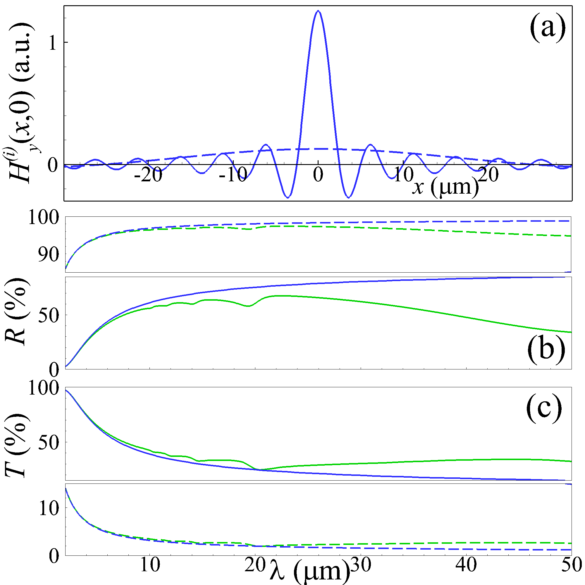 Figure 2
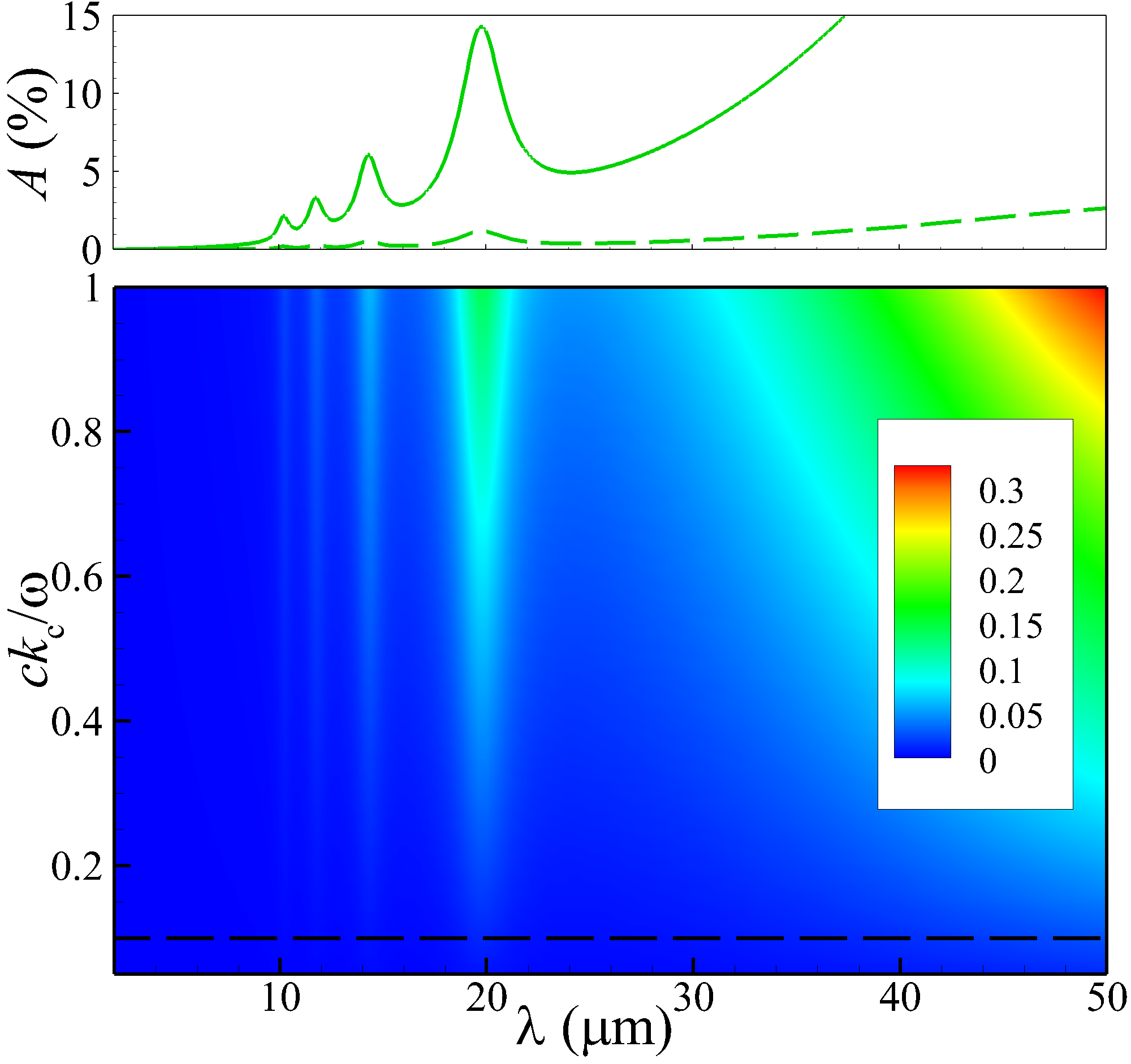 Figure 3
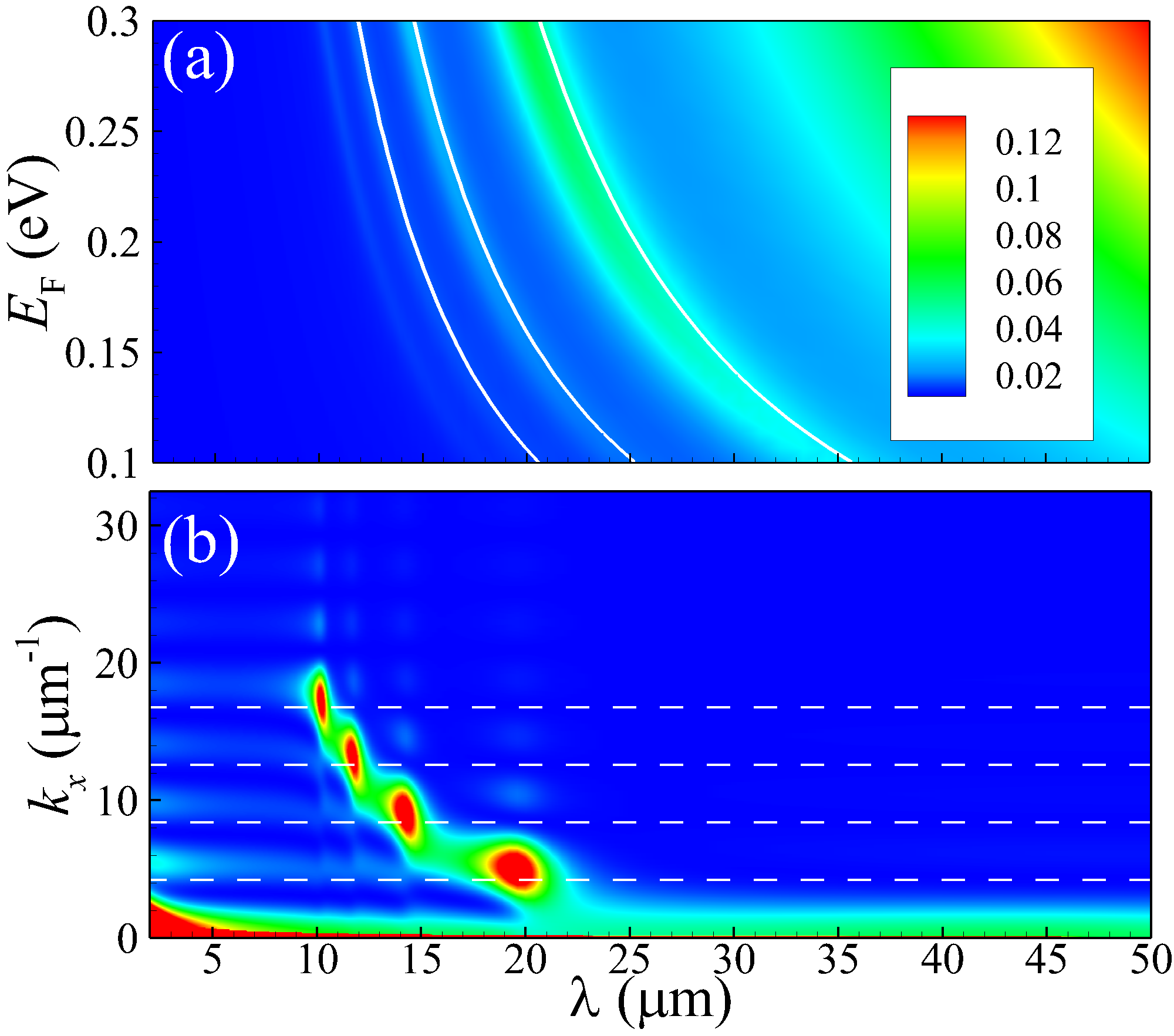 Figure 4
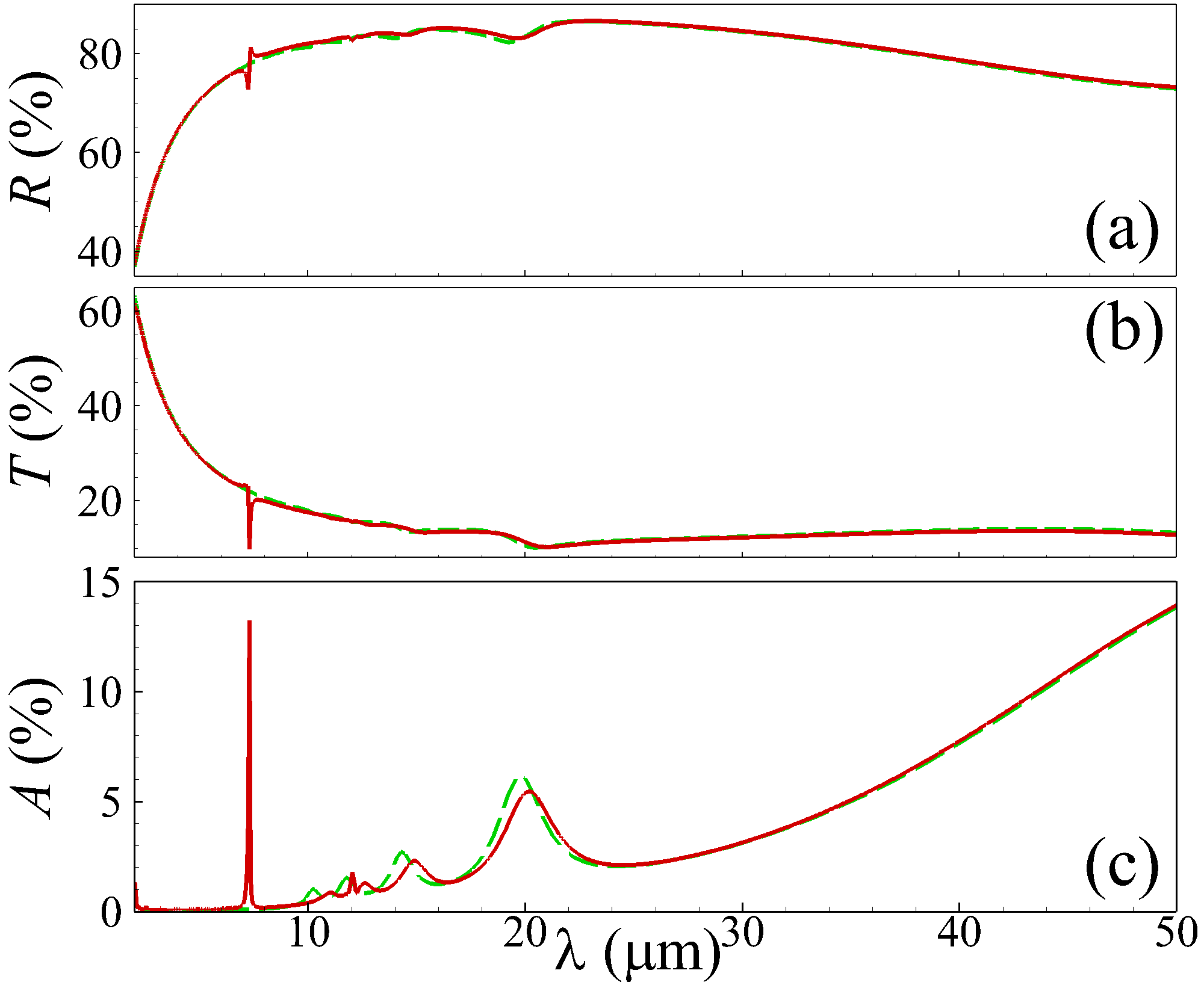 Figure 5
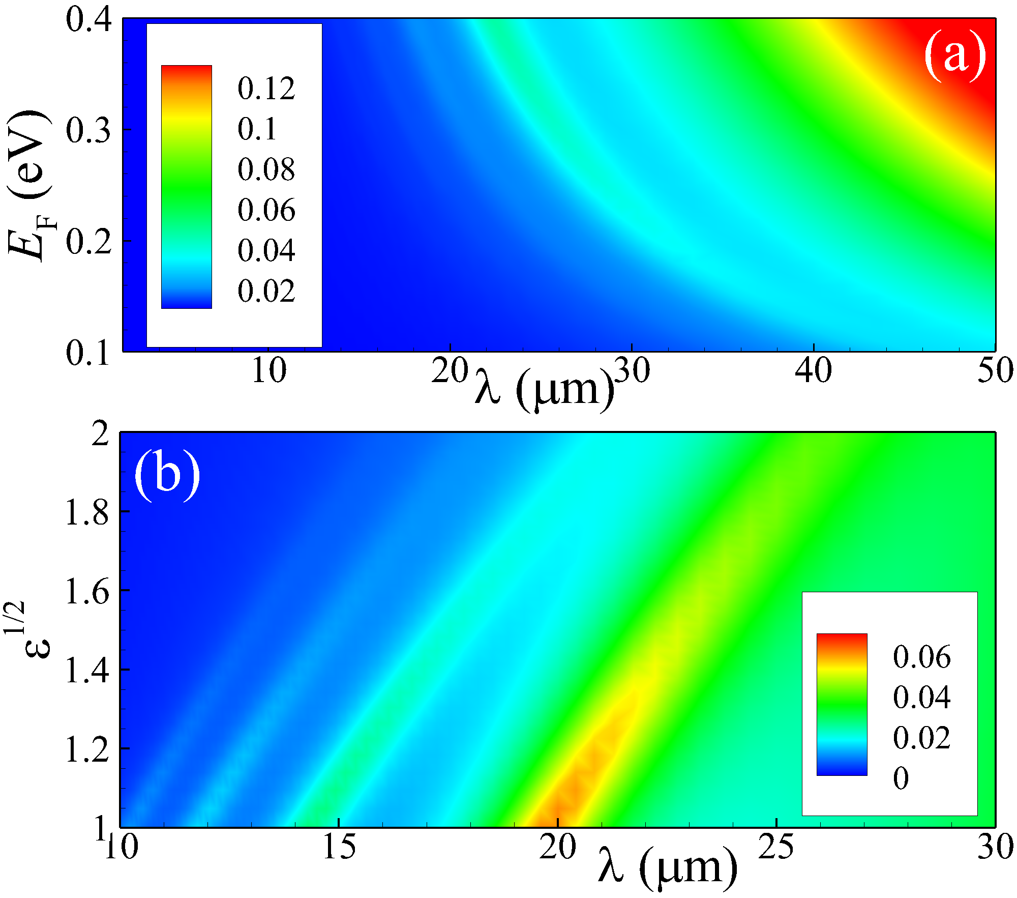 Figure 6
Peer Reviews
No public reviews on file for this paper yet. If you reviewed it on a platform where reviews are public (OpenReview, ICLR, NeurIPS, ICML), you can paste yours below so the community can read it here.
Videos
No videos yet. Explain this paper in a talk, walkthrough, or lecture? Add one.
Excitation of localized graphene plasmons by a metallic slit
Yu. V. Bludov1, N. M. R. Peres1,2, and M. I. Vasilevskiy1,2
1Department of Physics, Center of Physics, and QuantaLab, University of Minho, Campus of Gualtar, 4710-057, Braga, Portugal
2International Iberian Nanotechnology Laboratory (INL), Av. Mestre José Veiga, 4715-330 Braga, Portugal
Abstract
In this paper we show that graphene surface plasmons can be excited when an electromagnetic wave packet impinges on a single metal slit covered with graphene. The excitation of the plasmons localized over the slit is revealed by characteristic peaks in the absorption spectrum. It is shown that the position of the peaks can be tuned either by the graphene doping level or by the dielectric function of the material filling the slit. The whole system forms the basis for a plasmonic sensor when the slit is filled with an analyte.
I Introduction
The diffraction of electromagnetic (EM) waves on metallic structures gives rise to a series of interesting phenomena, such as the Wood and Rayleigh anomalies difr-slits-Wood1902-pm ; difr-slits-Rayleigh1907-prsa and the extraordinary optical transmission spp-eot-Ebessen1998-nat . Theoretical models for these phenomena have been elaborated by modelling the metal as perfect electric conductor (PEC), as in Refs. difr-slits-Porto1999-prl ; difr-slits-Sturman2011-prb ; grating-Maradudin2016-jopt . One of the fundamental problems in the nano-optics is the diffraction of light on a single slit of subwavelength width perforated in a metal. This kind of diffraction is accompanied by a series of effects such as funneling of the EM energy into the slit difr-slit-Sturman2010-prb ; difr-slit-Li2018-plasmonics and field enhancement inside it difr-slit-Sturman2010-prb , Fabri-Pérot resonances across the metallic film difr-slit-Takakura2001-prl ; difr-slit-exp-Yang2002-prl ; difr-slit-Bravo2004-pre , transmittance oscillations with an incidence angle variation in the geometrical optics limit difr-slit-Park1994-ieeetap and its absence in the subwavelength limitdifr-slit-Bravo2004-pre , and the sensitivity of the transmittance resonance frequencies to the refractive index of the material inside the slit difr-slit-Bravo2004-pre .
Consideration of the light diffraction on a single slit in real metals difr-slit-SPP-exp-Isaak2008-prb ; difr-slit-SPP-Chang2015-josabI ; difr-slit-SPP-Chang2015-josabII , with surface capable to supporting surface plasmon-polaritons (SPPs) enriches considerably the physics of the diffraction phenomena spp-rev-Barnes2003-nat . Nevertheless, SPPs in noble metals suffer from relatively high losses in the visible light wavelength, which considerably shorten their mean free path. One of the perspective ways to overcome this difficulty is to use graphene plasmons that can be combined with other materials in order to modify SPP’s properties spp-gr-rev-Bludov2013-ijmfb ; spp-gr-rev-deAbajo2014-ACSPhot ; spp-gr-rev-Low2014-ACSNano ; spp-gr-rev-Xiao2016-fp ; spp-gr-rev-Chen2017-nanophot ; spp-gr-rev-Luo2013-ssc .
As is well known, SPPs in graphene possess both large lifetime and high degree of field confinement spp-gr-Nikitin2011-prb ; spp-gr-rev-Koppens2011-nl . This property implies the advantage of using some kind of hybrid metal-graphene structures, where graphene sustains the propagation of SPPs, while PEC modifies their dispersion properties. For example, screening of graphene SPPs by a perfect spp-gr-acoustic-Principi2011-ssc ; spp-gr-acoustic-Gu2013-apl ; spp-gr-acoustic-exp-Alonso20016-nat or dispersive (Drude) spp-gr-acoustic-Polini2018-prb metal adjacent to it leads to the formation of acoustic SPPs with linear spectrum. Moreover, in such kind of structures SPP’s group velocity is quite low compared to polaritons in graphene on a thick dielectric substrate since high wavevectors correspond to relatively low frequencies in the SPP dispersion relation. The latter means that graphene’s conductivity exhibits its nonlocal properties in the THz frequency range and, therefore, gives rise to the nonlocal SPPs spp-gr-nonlocal-Horing2016 ; spp-gr-nonlocal-exp-Alcaraz2018-science ; spp-gr-nonlocal-Dias2018-prb ; spp-gr-nonlocal-exp-Koppens2017-science . Simultaneously, graphene’s conductivity (and, consequently, the dispersion properties of SPPs) can be effectively controlled by changing the applied gate voltage gr-cond-exp-Li2008-natp , which allows one to achieve the dynamical tunability of the resonant frequency in the graphene-based structures spp-gr-tunable-exp-Ju2011-nn ; spp-gr-tunable-Yao2014-nl ; spp-gr-tunable-exp-Fei2012-nat ; spp-gr-tunable-exp-Chen2012-nat ; spp-gr-tunable-exp-Alonso2014-nat . Being combined with a metallic grating, variation of gate voltage permits to control spoof plasmons spoof-Dias2017-ACSphot .
Since the dispersion properties of SPPs are extremely sensitive to the dielectric constant of the surrounding medium, plasmonics structures are widely used for molecular and biosensing spp-sensor-rev-Anker2008-natmat . The use of graphene in plasmonic biosensors spp-gr-sensor-Huang2017-pssa ; spp-gr-sensor-Meshginqalam2017-plasmonics has an additional advantage, since the above-mentioned tunability of the plasmonic resonance frequency allows for achive it in the spectral range where the strength of the characteristic molecular signal is the highest spp-gr-sensor-tunable-Hu2016-ncom .
Monochromatic plane waves are idealizations never realized in practice. The electromagnetic wave that impinges on the plasmonic structure and couples to SPPs (if the necessary conditions are fulfilled spp-gr-rev-Bludov2013-ijmfb ), generally is a wave packet, i.e. a superposition of plane waves with close but unequal frequencies and wavevectors, which may represent either a pulse or a focused beam Born-Wolf . In the present paper, we consider the diffraction of a localized wavepacket on the single rectangular slit in PEC film, which is covered by a graphene sheet encapsulated (that is, cladded) by two h-BN layers at one side and open on the other side (see Fig. 1). We demonstrate that the electromagnetic wave, when diffracted by the slit edges, excites a standing wave of SPPs in graphene at a series of resonant frequencies, which are determined by the graphene doping. At these resonance frequencies, the slit width contains an integer number of SPP wavelengths. Excitation of the polaritons yields a series of absorption peaks in the spectrum and these resonant frequencies turn out to be very sensitive to the dielectric constant of the dielectric material filling the slit, as it will be demostrated by our calculated results.
II Problem statement and main equations
II.1 The structure
We consider a graphene monolayer, located at plane and deposited on top of a h-BN layer of thickness that occupies the spatial domain . The graphene sheet is covered by another h-BN layer of the same thickness (). The lower h-BN layer is deposited on top of the PEC film of thickness (see Fig.1) with the surfaces located at and . The PEC film contains the single rectangular slit of width (), filled with a dielectric with the permittivity . We consider the incident wave packet propagating in the positive -axis direction, localized in the direction and impinging on the uppermost h-BN layer at normal incidence. Furthermore, it is essential that the wave packet is described by an even amplitude function of with respect to the vertical symmetry plane . To simplify the calculations, we shall consider the wave packet of a constant amplitude within a certain range of , , where , is the frequency and is the velocity of light in vacuum.
II.2 Maxwell equations and their solutions
Since the system under consideration is homogeneous in the direction (i.e., ), the Maxwell equations can be decoupled into two subsystems, which govern TM- and TE-polarized waves. In the following we will consider the case of TM-polarized waves only, which have the field components and . Assuming the EM field time-dependence as , we represent the Maxwell equations for the TM-polarized wave as
[TABLE]
The superscripts correspond to the spatial domains , , , and , respectively. The reason for such separation of the whole space into domains is that inside each domain the dielectric permittivity is homogeneous and generally is described by the diagonal tensor, in the coordinate frame of Fig. 1:
[TABLE]
In fact, in the isotropic media the tensor components are the same, for and (vacuum) equal to unity, , and for (isotropic dielectric) . The hexagonal boron nitride (spatial domains ) is a uniaxial medium with unequal tensor components in plane and out of plane, given by spp-hbn-Kumar2015-nl :
[TABLE]
Their depencence upon (in cm*-1*) is due to the polar optical phonon response and the numbers entering the above relations are the longitudinal and transverse optical phonon frequencies and the corresponding damping parameters; the multiplicative factors are the high-frequency dielectric constants.
Moreover, since both the geometry of the structure and the considered wave packet are symmetric with respect to the plane , we can seek the solution of the Maxwell equations (1) in the form of Fourier integrals over ,
[TABLE]
where and are the amplitudes of the -th harmonics of the tangential components of the magnetic and electric fields, respectively.
In the semi-infinite medium , the solution of Maxwell equation can be represented in the matrix form as
[TABLE]
Here
[TABLE]
is the field matrix, is the wavevector’s -component, and is the Heavyside function. For each line in Eq. (5), if written explicitly, the first term stands for the incident wavepacket with the amplitude and the cutoff in-plane wavevector , which propagates in the positive direction of -axis. Owing to this restriction, all waves constituting the incident wave packet have real -components of the wavevector. The second term for each line in Eq. (5) is the reflected wave, whose harmonics [with amplitudes ] can be either propagating in the negative direction of -axis (when ) or evanescent (when ) waves. Notice that the sign in the exponent for the evanescent waves is chosen to exclude the harmonics which grows at . At the same time, in the other semi-infinite spatial domain, (), the spectrum consist of transmitted waves only, with ],
[TABLE]
Again, these transmitted harmonics with amplitudes can be either propagating in the positive direction of the -axis or evanescent, decaying for .
In the finite spatial domain (medium ) the electromagnetic fields will be represented by means of the transfer matrix,
[TABLE]
as
[TABLE]
Here , which is the effective -component of the wavevector in a uniaxial medium DumelowParkerFarIRPhononsPlasmons . In Eq. (13), we represented the fields in the hBN substrate using values and [the EM field tangential components at ] as free parameters. This situation is distinct from the case of semi-infinite vacuum [see Eq. (5)], where the amplitudes of the reflected waves were used as free parameters. These free parameters will be eliminated by matching the fields at the interfaces.
In the medium (spatal domain ) the field structure is similar to that of Eq. (13) with the following replacement: (as a matter of fact, they are the same, i.e. ), , , and
[TABLE]
In other words,
[TABLE]
where the transfer-matrix is given by:
[TABLE]
In the medium the situation is quite different because the finite width of this domain in -direction imposes an additional boundary condition on the slit borders , namely the vanishing tangential component of the electric field . The solution of the Maxwell equations, satisfying these conditionscan be expressed as follows:
[TABLE]
[TABLE]
[TABLE]
where .
II.3 Boundary conditions
The problem in course includes four boundaries between aforementioned spatial domains, at which the fields in the neibouring domains are coupled by matching the boundary conditions. At the surface of the upper hBN layer (, boundary between spatial domains and ) the tangential components of the electric and magnetic fields must be continuous across the interface, i.e.
[TABLE]
At the interface between two hBN layers, where graphene layer is arranged (, boundary between media and ) the electric field tangential component is continuous across the interface, while the magnetic field tangentional component is discontinuous due to presence of two-dimensional currents in graphene,
[TABLE]
Taking into account the Ohm law, [where is the conductivity of the graphene, which in general case will be considered nonlocal, i.e. dependent upon the in-plane wavevector ], the boundary conditions can be expressed in the matrix form,
[TABLE]
with the matrix
[TABLE]
At the surfaces of the PEC film and (boundaries between the media and , respectively) the situation is more complicated. The tangential component of the magnetic field is continuous across the interfaces over the slit area,
[TABLE]
The tangential component of the electric field has to be continuous across the interfaces at the slit area and should vanish beyond the slit because the metal is assumed perfect. Therefore, boundary conditions can be expressed by the formulae
[TABLE]
It should be pointed out that, due to the fact that we use different bases of eignefunctions in medium and in media and , the boundary conditions (30)–(31) cannot be written in the same way as at boundaries and where they could be expressed separately for each spatial harmonic, and . Equations (30)–(31) involve the total fields in each point , , and involve all harmonics. In other words, these relations are integral equations. However, they can be discretized using the specific form of the fields inside the slit, Eqs. (21) and (22).
II.4 Amplitudes of the eignemodes inside the slit
Applying consequently boundary conditions (II.3) and (28) [jointly with expressions (5)–(19) for the fields in media ] one can obtain expressions for the electromagnetic field tangential components of each harmonic as
[TABLE]
where the total field matrix is composed from the transfer-matrices of media , boundary condition matrix across the graphene, and the field matrix in medium is:
[TABLE]
Substituting Eqs. (7), (21), (22), and (36) into boundary conditions (30)–(31) and using orthogonality relations between the dependence of the fields in the slit, Eqs. (21) and (22), and the harmonics (details are given in Supplementary Information), it is possible to obtain equations for the amplitudes of forward- and backward-propagating modes inside the slit, and :
[TABLE]
[TABLE]
where
[TABLE]
[TABLE]
and
[TABLE]
Now we consider a special case where the graphene layer is deposited directly over the slit (that is, both hBN layers are absent, i.e. ). Then
[TABLE]
As a consequence, Eq. (37) can be rewritten as
[TABLE]
where
[TABLE]
These equations also can be obtained from Eqs. (37) and (38) by taking . Notice that the integrals and can be calculated semi-analytically (see Supplementary Information).
The system of equations (38) and (40) was solved by truncating it to a sufficiently large order, and checking the convergence. Once the amplitudes have been found, the observable properties such as relectance and transmittance are calculated in a straightforward way (details are given in Supplementary Information).
III Suspended graphene
In order to clarify the influence of the graphene sheet on the transmittance and reflectance of the structure we consider first the situation where the slit is not filled (), and both hBN layers are absent. In other words, the graphene layer is deposited directly on the metal film and is suspended at the area of the slit.
From Fig. 2(a) it can be seen that a larger spectral width (solid line) correspond to a more focused beam in the coordinate space. As a consequence, the narrower beam (with larger ) exhibits a lower reflectance, , and a higher transmittance, [compare dashed and solid lines in Figs. 2(b) and 2(c)], because a larger fraction of the incident wave’s energy flux penetrates the slit, thus avoiding the diffraction on its edges. In the situation of bare slit [eV, blue lines in Figs. 2(b) and 2(c)] an increase of the wavelength, , leads to the growth of the reflectance [see Fig. 2(b)] and decrease of the transmittance [see Fig. 2(c)]. This phenomenon can be accounted for the essentially subwavelength character of the wavepacket diffraction. In fact, in the frequency range of Fig. 2 all the wavelengths of the wave packet are larger than the slit width. At the same time, for a larger ratio between the wavelength and the slit width, the presence of the slit exerts less influence on the diffraction process, thus the reflectance becomes more similar to that from a homogeneous PEC film, i.e. it increases to unity with the simultaneous decrease of the transmittance. When the slit is covered by doped graphene [eV, green lines in Figs. 2(b) and 2(c)], the aforementioned growth of the reflectance and decrease of transmittance in nonmonotonous, demonstrating the series of local minima.
Quite interesting are the absorption spectra of the considered structure. As can be seen from the upper panel of Fig. 3, the absorbance, , is high at the wavelengths corresponding to the reflectance and transmittance minima. Furtermore, a larger spectral width of the incident wavepacket () makes these absorbance peaks more pronounced [see lower panel of Fig. 3], while their positions (wavelengths ) are not affected. At the same time, the positions of the absorption peaks are strongly influenced by the graphene’s Fermi energy [see Fig. 4(a)]. This fact resembles the crucial property of graphene SPPs whose dispersion curve, , scales with the Fermi energy approximately as for small . A more detailed analysis leads to the following expression for the characteristic wavelengths of the SPP eigenmodes:
[TABLE]
where and stands for the fine structure constant. These modes are depicted the white solid lines in Fig. 4(a). The polaritonic character of the absorption peaks are confirmed by the fact that the spectral positions of the absorbance maxima coincide with the graphene SPP eigenmodes. Moreover, the modulus of the electric field of the reflected wave harmonics [depicted in Fig. 4(b)] has its maxima near the resonance wavelengths, [Eq. (41)]. The associated wavevectors [horizonal dashed lines in Fig. 4(b)] correspond to the even spatial profiles of the tangential components of the eigenmode’s electromagnetic field inside the slit [see Eqs. (21), (22)]. In other words, when the incident wave packet’s wavelength coincides with the wavelength of an SPP eigenmode with the wavevector , the wave packet, being diffracted on the slit, resonantly excites SPPs in graphene. This polariton, owing to the multiple reflections from the slit edges, forms the SPP standing wave in the suspended graphene with the nodes of its electric field (-component) at the edges of the slit. This resonant excitation leads to the transformation of incident wave packet’s energy into the energy of the with eV standing wave; this phenomenon gives rise to the resonant absorption.
Qualitatively, the situation here is similar to the structure composed of non-absorbing nanoparticles (NPs) deposited on a homogeneous graphene sheet, where the symmetry breaking caused by the NPs induces surface plasmon-polaritons and originates absorption of propagating EM waves due to energy dissipation by the graphene plasmons Santos2014 . Indeed, the absorbance spectra of Fig. 2 show a similarity to that of the ”graphene + NPs” system Santos2014 , although here we observe not just the lowest energy (longest wavelength) absorption peak but also its overtones according to Eq. (41).
IV Effect of the substrate
The essential physics behind the optical properties of the graphene-covered slit has been established in the previous section and now we may address a further question, how will the results change if the graphene is not deposited directly on the metal film but rather cladded by two hBN layers as depicted in Fig. 1? To answer this question, in Fig. 5 we present a comparison of the reflectance, transmittance, and absorbance of the suspended (dashed green lines) and hBN-encapsulated graphene (solid red lines). As can be seen from the comparison of the dashed and solid lines in Fig. 5, the presence of hBN leads to the small shift of the positions of the SPP absorbance maxima, and the appearance of two additional maxima (nearby m and m) due to the excitation of optical phonons in the hBN cladding layers.
One of the crucial properties of SPPs is the strong sensitivity of their dispersion to the dielectric constants of the surrounding media, which should also apply to the dielectric filling the slit in the present case. Therefore, Fig. 6(a) presents the absorbance of the graphene layer deposited over the slit filled by a material with the dielectric constant . As it follows from the comparison of Figs. 6(a) and 4(a), the presence of the dielectric inside the slit results in a red shift of the plasmonic absorption peaks. In more detail this phenomenon is demonstrated in Fig. 6(b). As it can be seen from this plot, there is an almost linear dependence of the plasmonic absorption peak positions upon the refractive index, . Even more, when the refractive index is changed in the limits between 1 and 2, the plasmonic absorption peak wavelength is shifted by m.
This phenomenon can be used in plasmonic sensors. The advantage of the graphene-based plasmonic sensor is an additional degree of its dynamical tunability. Thus, if a source of electromagnetic readiation with a fixed wavelength is used, then the position of the plasmonic absorption peak can be tuned to the desired wavelength by adjusting the graphene’s Fermi energy and its value can provide information about the dielectric constant of the medium that fills the slit.
V Conclusion
To conclude, we considered the diffraction of the spatially localized wavepacket on the single slit in a perfect metalic film covered by monolayer graphene. We have shown that this geometry is suitable for the excitation of surface plasmon-polaritons in graphene. The diffraction of the wavepacket on the slit is accompanied by the excitation of the polariton standing wave, for which the vertical edges of the slit in PEC serve as a cavity. The resonance condition for the excitation of such standing waves can be expressed in the following manner: the excitation of SPP takes place for a given frequency of the incident wavepacket, , if the slit width contains an integer number of the polariton wavelengths, , where is the SPP wavevector for the frequency .
The excitation of SPPs is manifested by the appearance of the peaks in the absorbance spectrum. Also the positions of these resonant absorption peaks can be effectively tuned by the electrostatic gating of graphene. The resonant frequencies are shown to be very sensitive to the refractive index of the medium, which fills the slit. This phenomenon can be used for environment sensing. The advantage of the such graphene-based sensor is the possibility to tune (by the graphene gating) the position of the absorption peaks to the spectral range where the fingerprints of the molecules are the most intense, e.g. due to the presence of dipolar vibration modes.
Acknowledgements
Authors acknowledge support from the European Commission through the project ”Graphene- Driven Revolutions in ICT and Beyond” (Ref. No. 785219), and the Portuguese Foundation for Science and Technology through the Strategic Funding UID/FIS/04650/2019. Additionally, authors acknowledge financing from FEDER and the portuguese Foundation for Science and Technology (FCT) through project POCI-01-0145-FEDER-028114.
The reference list from the paper itself. Each links out to its DOI / PubMed record.
- 1[1] R.W. Wood. XLII. On a remarkable case of uneven distribution of light in a diffraction grating spectrum. Phil. Mag. , 4(21):396–402, sep 1902.
- 2[2] L. Rayleigh. On the Dynamical Theory of Gratings. Proceedings of the Royal Society A: Mathematical, Physical and Engineering Sciences , 79(532):399–416, aug 1907.
- 3[3] T. W. Ebbesen, H. J. Lezec, H. F. Ghaemi, T. Thio, and P. A. Wolff. Extraordinary optical transmission through sub-wavelength hole arrays. Nature , 391(6668):667–669, feb 1998.
- 4[4] J A Porto, F. J. García-Vidal, and J. B. Pendry. Transmission Resonances on Metallic Gratings with Very Narrow Slits. Physical Review Letters , 83(14):2845–2848, oct 1999.
- 5[5] B. Sturman, E. Podivilov, and M. Gorkunov. Optical properties of periodic arrays of subwavelength slits in a perfect metal. Physical Review B , 84(20):205439, nov 2011.
- 6[6] A. A. Maradudin, I. Simonsen, J. Polanco, and R. M. Fitzgerald. Rayleigh and Wood anomalies in the diffraction of light from a perfectly conducting reflection grating. Journal of Optics , 18(2):024004, feb 2016.
- 7[7] B. Sturman, E. Podivilov, and M. Gorkunov. Transmission and diffraction properties of a narrow slit in a perfect metal. Physical Review B , 82(11):115419, sep 2010.
- 8[8] Jing-Wei Li, Jian-Shiung Hong, Wei-Ting Chou, Ding-Jie Huang, and Kuan-Ren Chen. Light Funneling Profile During Enhanced Transmission Through a Subwavelength Metallic Slit. Plasmonics , 13(6):2249–2254, dec 2018.